Freescale 高级S12系列单片机编程
HCS12X微控制器Freescale MC9S12XHZ512数据手册说明书

MC9S12XHZ512Data SheetCoversMC9S12XHZ384, MC9S12XHZ256 HCS12XMicrocontrollersMC9S12XHZ512Rev. 1.0610/2010To provide the most up-to-date information,the revision of our documents on the World Wide Web will be the most current.Your printed copy may be an earlier revision.To verify you have the latest information available, refer to:/The following revision history table summarizes changes contained in this document. This document contains information for all constituent modules, with the exception of the S12X CPU. For S12X CPU information please refer to CPU12XV2 in the CPU12/CPU12X Reference Manual.Revision HistoryDate RevisionLevelDescriptionJanuary 5, 200601.00New BookApril 20, 200601.01Updated block guide versionsJuly 28, 200601.02Made minor correctionsJanuary 8, 200701.03Added MC9S12XHZ384 and MC9S12XHZ256August 20, 200701.04Updated slew ratesNovember 4, 200801.05Corrected typos on pinout diagramOctober 14, 201001.06Added PartID. Minor updates to ECT, SCI, IIC and XGATE sections.List of ChaptersChapter1MC9S12XHZ Family Device Overview . . . . . . . . . . . . . . . . . . .21 Chapter2Port Integration Module (S12XHZPIMV1). . . . . . . . . . . . . . . . .57 Chapter3512 Kbyte Flash Module (S12XFTX512K4V3). . . . . . . . . . . . .131 Chapter4 4 Kbyte EEPROM Module (S12XEETX4KV2) . . . . . . . . . . . . .175 Chapter5XGATE (S12XGATEV2). . . . . . . . . . . . . . . . . . . . . . . . . . . . . . .209 Chapter6Security (S12X9SECV2) . . . . . . . . . . . . . . . . . . . . . . . . . . . . .323 Chapter7Clocks and Reset Generator (S12CRGV6). . . . . . . . . . . . . . .331 Chapter8Pierce Oscillator (S12XOSCLCPV1) . . . . . . . . . . . . . . . . . . . .371 Chapter9Analog-to-Digital Converter (ATD10B16CV4) . . . . . . . . . . . .377 Chapter10Liquid Crystal Display (LCD32F4BV1) . . . . . . . . . . . . . . . . . .411 Chapter11Motor Controller (MC10B12CV2). . . . . . . . . . . . . . . . . . . . . . .429 Chapter12Stepper Stall Detector (SSDV1). . . . . . . . . . . . . . . . . . . . . . . .461 Chapter13Inter-Integrated Circuit (IICV3) . . . . . . . . . . . . . . . . . . . . . . . .479 Chapter14Freescale’s Scalable Controller Area Network (MSCANV3).507 Chapter15Serial Communication Interface (SCIV5) . . . . . . . . . . . . . . . .561 Chapter16Serial Peripheral Interface (SPIV4) . . . . . . . . . . . . . . . . . . . . .599 Chapter17Periodic Interrupt Timer (PIT24B4CV1) . . . . . . . . . . . . . . . . .625 Chapter18Pulse-Width Modulator (PWM8B8CV1). . . . . . . . . . . . . . . . . .639 Chapter19Enhanced Capture Timer (ECT16B8CV3). . . . . . . . . . . . . . . .671 Chapter20Voltage Regulator (VREG3V3V5) . . . . . . . . . . . . . . . . . . . . . .725 Chapter21Background Debug Module (S12XBDMV2) . . . . . . . . . . . . . .739 Chapter22S12X Debug (S12XDBGV3) Module . . . . . . . . . . . . . . . . . . . .765 Chapter23External Bus Interface (S12XEBIV3). . . . . . . . . . . . . . . . . . . .807 Chapter24Interrupt (S12XINTV1) . . . . . . . . . . . . . . . . . . . . . . . . . . . . . . .831 Chapter25Memory Mapping Control (S12XMMCV3). . . . . . . . . . . . . . . .849Appendix A Electrical Characteristics. . . . . . . . . . . . . . . . . . . . . . . . . . . . .891 Appendix B Package Information . . . . . . . . . . . . . . . . . . . . . . . . . . . . . . . .935 Appendix C PCB Layout Guidelines . . . . . . . . . . . . . . . . . . . . . . . . . . . . . .938 Appendix D Ordering Information . . . . . . . . . . . . . . . . . . . . . . . . . . . . . . . .941 Appendix E Detailed Register Map . . . . . . . . . . . . . . . . . . . . . . . . . . . . . . .942Table of ContentsChapter1MC9S12XHZ Family Device Overview1.1Introduction . . . . . . . . . . . . . . . . . . . . . . . . . . . . . . . . . . . . . . . . . . . . . . . . . . . . . . . . . . . . . . . . . .211.1.1Features . . . . . . . . . . . . . . . . . . . . . . . . . . . . . . . . . . . . . . . . . . . . . . . . . . . . . . . . . . . . . .221.1.2Modes of Operation. . . . . . . . . . . . . . . . . . . . . . . . . . . . . . . . . . . . . . . . . . . . . . . . . . . . .241.1.3Block Diagram. . . . . . . . . . . . . . . . . . . . . . . . . . . . . . . . . . . . . . . . . . . . . . . . . . . . . . . . .241.1.4Device Memory Map. . . . . . . . . . . . . . . . . . . . . . . . . . . . . . . . . . . . . . . . . . . . . . . . . . . .261.1.5Part ID Assignments . . . . . . . . . . . . . . . . . . . . . . . . . . . . . . . . . . . . . . . . . . . . . . . . . . . .30 1.2Signal Description . . . . . . . . . . . . . . . . . . . . . . . . . . . . . . . . . . . . . . . . . . . . . . . . . . . . . . . . . . . . .301.2.1Device Pinout. . . . . . . . . . . . . . . . . . . . . . . . . . . . . . . . . . . . . . . . . . . . . . . . . . . . . . . . . .301.2.2Signal Properties Summary . . . . . . . . . . . . . . . . . . . . . . . . . . . . . . . . . . . . . . . . . . . . . . .331.2.3Detailed Signal Descriptions . . . . . . . . . . . . . . . . . . . . . . . . . . . . . . . . . . . . . . . . . . . . . .361.2.4Power Supply Pins. . . . . . . . . . . . . . . . . . . . . . . . . . . . . . . . . . . . . . . . . . . . . . . . . . . . . .45 1.3System Clock Description . . . . . . . . . . . . . . . . . . . . . . . . . . . . . . . . . . . . . . . . . . . . . . . . . . . . . . .47 1.4Chip Configuration Summary . . . . . . . . . . . . . . . . . . . . . . . . . . . . . . . . . . . . . . . . . . . . . . . . . . . .48 1.5Modes of Operation . . . . . . . . . . . . . . . . . . . . . . . . . . . . . . . . . . . . . . . . . . . . . . . . . . . . . . . . . . . .491.5.1User Modes . . . . . . . . . . . . . . . . . . . . . . . . . . . . . . . . . . . . . . . . . . . . . . . . . . . . . . . . . . .491.5.2Low-Power Modes. . . . . . . . . . . . . . . . . . . . . . . . . . . . . . . . . . . . . . . . . . . . . . . . . . . . . .501.5.3Freeze Mode. . . . . . . . . . . . . . . . . . . . . . . . . . . . . . . . . . . . . . . . . . . . . . . . . . . . . . . . . . .51 1.6Resets and Interrupts . . . . . . . . . . . . . . . . . . . . . . . . . . . . . . . . . . . . . . . . . . . . . . . . . . . . . . . . . . .511.6.1Vectors . . . . . . . . . . . . . . . . . . . . . . . . . . . . . . . . . . . . . . . . . . . . . . . . . . . . . . . . . . . . . . .511.6.2Effects of Reset . . . . . . . . . . . . . . . . . . . . . . . . . . . . . . . . . . . . . . . . . . . . . . . . . . . . . . . .54 1.7COP Configuration. . . . . . . . . . . . . . . . . . . . . . . . . . . . . . . . . . . . . . . . . . . . . . . . . . . . . . . . . . . . .54 1.8ATD External Trigger Input Connection . . . . . . . . . . . . . . . . . . . . . . . . . . . . . . . . . . . . . . . . . . . .55Chapter2Port Integration Module (S12XHZPIMV1)2.1lntroduction . . . . . . . . . . . . . . . . . . . . . . . . . . . . . . . . . . . . . . . . . . . . . . . . . . . . . . . . . . . . . . . . . .572.1.1Features . . . . . . . . . . . . . . . . . . . . . . . . . . . . . . . . . . . . . . . . . . . . . . . . . . . . . . . . . . . . . .572.1.2Block Diagram. . . . . . . . . . . . . . . . . . . . . . . . . . . . . . . . . . . . . . . . . . . . . . . . . . . . . . . . .58 2.2External Signal Description. . . . . . . . . . . . . . . . . . . . . . . . . . . . . . . . . . . . . . . . . . . . . . . . . . . . . .59 2.3Memory Map and Register Definition . . . . . . . . . . . . . . . . . . . . . . . . . . . . . . . . . . . . . . . . . . . . . .652.3.1Port A and Port B. . . . . . . . . . . . . . . . . . . . . . . . . . . . . . . . . . . . . . . . . . . . . . . . . . . . . . .682.3.2Port C and Port D. . . . . . . . . . . . . . . . . . . . . . . . . . . . . . . . . . . . . . . . . . . . . . . . . . . . . . .712.3.3Port E. . . . . . . . . . . . . . . . . . . . . . . . . . . . . . . . . . . . . . . . . . . . . . . . . . . . . . . . . . . . . . . .732.3.4Port K. . . . . . . . . . . . . . . . . . . . . . . . . . . . . . . . . . . . . . . . . . . . . . . . . . . . . . . . . . . . . . . .752.3.5Miscellaneous registers . . . . . . . . . . . . . . . . . . . . . . . . . . . . . . . . . . . . . . . . . . . . . . . . . .772.3.6Port AD . . . . . . . . . . . . . . . . . . . . . . . . . . . . . . . . . . . . . . . . . . . . . . . . . . . . . . . . . . . . . .822.3.7Port L. . . . . . . . . . . . . . . . . . . . . . . . . . . . . . . . . . . . . . . . . . . . . . . . . . . . . . . . . . . . . . . .872.3.8Port M . . . . . . . . . . . . . . . . . . . . . . . . . . . . . . . . . . . . . . . . . . . . . . . . . . . . . . . . . . . . . . .912.3.9Port P . . . . . . . . . . . . . . . . . . . . . . . . . . . . . . . . . . . . . . . . . . . . . . . . . . . . . . . . . . . . . . . .962.3.10Port S . . . . . . . . . . . . . . . . . . . . . . . . . . . . . . . . . . . . . . . . . . . . . . . . . . . . . . . . . . . . . . .1022.3.11Port T. . . . . . . . . . . . . . . . . . . . . . . . . . . . . . . . . . . . . . . . . . . . . . . . . . . . . . . . . . . . . . .1072.3.12Port U. . . . . . . . . . . . . . . . . . . . . . . . . . . . . . . . . . . . . . . . . . . . . . . . . . . . . . . . . . . . . . .1132.3.13Port V. . . . . . . . . . . . . . . . . . . . . . . . . . . . . . . . . . . . . . . . . . . . . . . . . . . . . . . . . . . . . . .1172.3.14Port W . . . . . . . . . . . . . . . . . . . . . . . . . . . . . . . . . . . . . . . . . . . . . . . . . . . . . . . . . . . . . .121 2.4Functional Description. . . . . . . . . . . . . . . . . . . . . . . . . . . . . . . . . . . . . . . . . . . . . . . . . . . . . . . . .1252.4.1I/O Register . . . . . . . . . . . . . . . . . . . . . . . . . . . . . . . . . . . . . . . . . . . . . . . . . . . . . . . . . .1252.4.2Input Register. . . . . . . . . . . . . . . . . . . . . . . . . . . . . . . . . . . . . . . . . . . . . . . . . . . . . . . . .1252.4.3Data Direction Register . . . . . . . . . . . . . . . . . . . . . . . . . . . . . . . . . . . . . . . . . . . . . . . . .1262.4.4Reduced Drive Register. . . . . . . . . . . . . . . . . . . . . . . . . . . . . . . . . . . . . . . . . . . . . . . . .1272.4.5Pull Device Enable Register . . . . . . . . . . . . . . . . . . . . . . . . . . . . . . . . . . . . . . . . . . . . .1272.4.6Polarity Select Register . . . . . . . . . . . . . . . . . . . . . . . . . . . . . . . . . . . . . . . . . . . . . . . . .1272.4.7Pin Configuration Summary . . . . . . . . . . . . . . . . . . . . . . . . . . . . . . . . . . . . . . . . . . . . .127 2.5Resets. . . . . . . . . . . . . . . . . . . . . . . . . . . . . . . . . . . . . . . . . . . . . . . . . . . . . . . . . . . . . . . . . . . . . .1282.5.1Reset Initialization. . . . . . . . . . . . . . . . . . . . . . . . . . . . . . . . . . . . . . . . . . . . . . . . . . . . .128 2.6Interrupts . . . . . . . . . . . . . . . . . . . . . . . . . . . . . . . . . . . . . . . . . . . . . . . . . . . . . . . . . . . . . . . . . . .1292.6.1General. . . . . . . . . . . . . . . . . . . . . . . . . . . . . . . . . . . . . . . . . . . . . . . . . . . . . . . . . . . . . .1292.6.2Interrupt Sources . . . . . . . . . . . . . . . . . . . . . . . . . . . . . . . . . . . . . . . . . . . . . . . . . . . . . .1302.6.3Operation in Stop Mode. . . . . . . . . . . . . . . . . . . . . . . . . . . . . . . . . . . . . . . . . . . . . . . . .130Chapter3512 Kbyte Flash Module (S12XFTX512K4V3)3.1Introduction . . . . . . . . . . . . . . . . . . . . . . . . . . . . . . . . . . . . . . . . . . . . . . . . . . . . . . . . . . . . . . . . .1313.1.1Glossary. . . . . . . . . . . . . . . . . . . . . . . . . . . . . . . . . . . . . . . . . . . . . . . . . . . . . . . . . . . . .1313.1.2Features . . . . . . . . . . . . . . . . . . . . . . . . . . . . . . . . . . . . . . . . . . . . . . . . . . . . . . . . . . . . .1313.1.3Modes of Operation. . . . . . . . . . . . . . . . . . . . . . . . . . . . . . . . . . . . . . . . . . . . . . . . . . . .1323.1.4Block Diagram. . . . . . . . . . . . . . . . . . . . . . . . . . . . . . . . . . . . . . . . . . . . . . . . . . . . . . . .132 3.2External Signal Description. . . . . . . . . . . . . . . . . . . . . . . . . . . . . . . . . . . . . . . . . . . . . . . . . . . . .133 3.3Memory Map and Register Definition . . . . . . . . . . . . . . . . . . . . . . . . . . . . . . . . . . . . . . . . . . . . .1343.3.1Module Memory Map . . . . . . . . . . . . . . . . . . . . . . . . . . . . . . . . . . . . . . . . . . . . . . . . . .1343.3.2Register Descriptions. . . . . . . . . . . . . . . . . . . . . . . . . . . . . . . . . . . . . . . . . . . . . . . . . . .136 3.4Functional Description. . . . . . . . . . . . . . . . . . . . . . . . . . . . . . . . . . . . . . . . . . . . . . . . . . . . . . . . .1503.4.1Flash Command Operations. . . . . . . . . . . . . . . . . . . . . . . . . . . . . . . . . . . . . . . . . . . . . .1503.4.2Flash Commands . . . . . . . . . . . . . . . . . . . . . . . . . . . . . . . . . . . . . . . . . . . . . . . . . . . . . .1533.4.3Illegal Flash Operations. . . . . . . . . . . . . . . . . . . . . . . . . . . . . . . . . . . . . . . . . . . . . . . . .169 3.5Operating Modes . . . . . . . . . . . . . . . . . . . . . . . . . . . . . . . . . . . . . . . . . . . . . . . . . . . . . . . . . . . . .1703.5.1Wait Mode . . . . . . . . . . . . . . . . . . . . . . . . . . . . . . . . . . . . . . . . . . . . . . . . . . . . . . . . . . .1703.5.2Stop Mode . . . . . . . . . . . . . . . . . . . . . . . . . . . . . . . . . . . . . . . . . . . . . . . . . . . . . . . . . . .1703.5.3Background Debug Mode . . . . . . . . . . . . . . . . . . . . . . . . . . . . . . . . . . . . . . . . . . . . . . .1703.6Flash Module Security. . . . . . . . . . . . . . . . . . . . . . . . . . . . . . . . . . . . . . . . . . . . . . . . . . . . . . . . .1703.6.1Unsecuring the MCU using Backdoor Key Access. . . . . . . . . . . . . . . . . . . . . . . . . . . .1713.6.2Unsecuring the MCU in Special Single Chip Mode using BDM . . . . . . . . . . . . . . . . .172 3.7Resets. . . . . . . . . . . . . . . . . . . . . . . . . . . . . . . . . . . . . . . . . . . . . . . . . . . . . . . . . . . . . . . . . . . . . .1723.7.1Flash Reset Sequence. . . . . . . . . . . . . . . . . . . . . . . . . . . . . . . . . . . . . . . . . . . . . . . . . . .1723.7.2Reset While Flash Command Active. . . . . . . . . . . . . . . . . . . . . . . . . . . . . . . . . . . . . . .172 3.8Interrupts . . . . . . . . . . . . . . . . . . . . . . . . . . . . . . . . . . . . . . . . . . . . . . . . . . . . . . . . . . . . . . . . . . .1723.8.1Description of Flash Interrupt Operation. . . . . . . . . . . . . . . . . . . . . . . . . . . . . . . . . . . .173Chapter44 Kbyte EEPROM Module (S12XEETX4KV2)4.1Introduction . . . . . . . . . . . . . . . . . . . . . . . . . . . . . . . . . . . . . . . . . . . . . . . . . . . . . . . . . . . . . . . . .1754.1.1Glossary. . . . . . . . . . . . . . . . . . . . . . . . . . . . . . . . . . . . . . . . . . . . . . . . . . . . . . . . . . . . .1754.1.2Features . . . . . . . . . . . . . . . . . . . . . . . . . . . . . . . . . . . . . . . . . . . . . . . . . . . . . . . . . . . . .1754.1.3Modes of Operation. . . . . . . . . . . . . . . . . . . . . . . . . . . . . . . . . . . . . . . . . . . . . . . . . . . .1754.1.4Block Diagram. . . . . . . . . . . . . . . . . . . . . . . . . . . . . . . . . . . . . . . . . . . . . . . . . . . . . . . .176 4.2External Signal Description. . . . . . . . . . . . . . . . . . . . . . . . . . . . . . . . . . . . . . . . . . . . . . . . . . . . .176 4.3Memory Map and Register Definition . . . . . . . . . . . . . . . . . . . . . . . . . . . . . . . . . . . . . . . . . . . . .1764.3.1Module Memory Map . . . . . . . . . . . . . . . . . . . . . . . . . . . . . . . . . . . . . . . . . . . . . . . . . .1764.3.2Register Descriptions. . . . . . . . . . . . . . . . . . . . . . . . . . . . . . . . . . . . . . . . . . . . . . . . . . .179 4.4Functional Description. . . . . . . . . . . . . . . . . . . . . . . . . . . . . . . . . . . . . . . . . . . . . . . . . . . . . . . . .1874.4.1EEPROM Command Operations. . . . . . . . . . . . . . . . . . . . . . . . . . . . . . . . . . . . . . . . . .1874.4.2EEPROM Commands . . . . . . . . . . . . . . . . . . . . . . . . . . . . . . . . . . . . . . . . . . . . . . . . . .1904.4.3Illegal EEPROM Operations . . . . . . . . . . . . . . . . . . . . . . . . . . . . . . . . . . . . . . . . . . . . .204 4.5Operating Modes . . . . . . . . . . . . . . . . . . . . . . . . . . . . . . . . . . . . . . . . . . . . . . . . . . . . . . . . . . . . .2054.5.1Wait Mode . . . . . . . . . . . . . . . . . . . . . . . . . . . . . . . . . . . . . . . . . . . . . . . . . . . . . . . . . . .2054.5.2Stop Mode . . . . . . . . . . . . . . . . . . . . . . . . . . . . . . . . . . . . . . . . . . . . . . . . . . . . . . . . . . .2054.5.3Background Debug Mode . . . . . . . . . . . . . . . . . . . . . . . . . . . . . . . . . . . . . . . . . . . . . . .205 4.6EEPROM Module Security . . . . . . . . . . . . . . . . . . . . . . . . . . . . . . . . . . . . . . . . . . . . . . . . . . . . .2054.6.1Unsecuring the MCU in Special Single Chip Mode using BDM . . . . . . . . . . . . . . . . .206 4.7Resets. . . . . . . . . . . . . . . . . . . . . . . . . . . . . . . . . . . . . . . . . . . . . . . . . . . . . . . . . . . . . . . . . . . . . .2064.7.1EEPROM Reset Sequence. . . . . . . . . . . . . . . . . . . . . . . . . . . . . . . . . . . . . . . . . . . . . . .2064.7.2Reset While EEPROM Command Active . . . . . . . . . . . . . . . . . . . . . . . . . . . . . . . . . . .206 4.8Interrupts . . . . . . . . . . . . . . . . . . . . . . . . . . . . . . . . . . . . . . . . . . . . . . . . . . . . . . . . . . . . . . . . . . .2064.8.1Description of EEPROM Interrupt Operation. . . . . . . . . . . . . . . . . . . . . . . . . . . . . . . .207Chapter5XGATE (S12XGATEV2)5.1Introduction . . . . . . . . . . . . . . . . . . . . . . . . . . . . . . . . . . . . . . . . . . . . . . . . . . . . . . . . . . . . . . . . .2095.1.1Glossary of Terms . . . . . . . . . . . . . . . . . . . . . . . . . . . . . . . . . . . . . . . . . . . . . . . . . . . . .2095.1.2Features . . . . . . . . . . . . . . . . . . . . . . . . . . . . . . . . . . . . . . . . . . . . . . . . . . . . . . . . . . . . .2105.1.3Modes of Operation. . . . . . . . . . . . . . . . . . . . . . . . . . . . . . . . . . . . . . . . . . . . . . . . . . . .2115.1.4Block Diagram. . . . . . . . . . . . . . . . . . . . . . . . . . . . . . . . . . . . . . . . . . . . . . . . . . . . . . . .211 5.2External Signal Description. . . . . . . . . . . . . . . . . . . . . . . . . . . . . . . . . . . . . . . . . . . . . . . . . . . . .212 5.3Memory Map and Register Definition . . . . . . . . . . . . . . . . . . . . . . . . . . . . . . . . . . . . . . . . . . . . .2135.3.1Register Descriptions. . . . . . . . . . . . . . . . . . . . . . . . . . . . . . . . . . . . . . . . . . . . . . . . . . .213 5.4Functional Description. . . . . . . . . . . . . . . . . . . . . . . . . . . . . . . . . . . . . . . . . . . . . . . . . . . . . . . . .2295.4.1XGATE RISC Core . . . . . . . . . . . . . . . . . . . . . . . . . . . . . . . . . . . . . . . . . . . . . . . . . . . .2295.4.2Programmer’s Model. . . . . . . . . . . . . . . . . . . . . . . . . . . . . . . . . . . . . . . . . . . . . . . . . . .2295.4.3Memory Map. . . . . . . . . . . . . . . . . . . . . . . . . . . . . . . . . . . . . . . . . . . . . . . . . . . . . . . . .2305.4.4Semaphores . . . . . . . . . . . . . . . . . . . . . . . . . . . . . . . . . . . . . . . . . . . . . . . . . . . . . . . . . .2315.4.5Software Error Detection. . . . . . . . . . . . . . . . . . . . . . . . . . . . . . . . . . . . . . . . . . . . . . . .232 5.5Interrupts . . . . . . . . . . . . . . . . . . . . . . . . . . . . . . . . . . . . . . . . . . . . . . . . . . . . . . . . . . . . . . . . . . .2335.5.1Incoming Interrupt Requests . . . . . . . . . . . . . . . . . . . . . . . . . . . . . . . . . . . . . . . . . . . . .2335.5.2Outgoing Interrupt Requests . . . . . . . . . . . . . . . . . . . . . . . . . . . . . . . . . . . . . . . . . . . . .233 5.6Debug Mode. . . . . . . . . . . . . . . . . . . . . . . . . . . . . . . . . . . . . . . . . . . . . . . . . . . . . . . . . . . . . . . . .2335.6.1Debug Features . . . . . . . . . . . . . . . . . . . . . . . . . . . . . . . . . . . . . . . . . . . . . . . . . . . . . . .2335.6.2Entering Debug Mode . . . . . . . . . . . . . . . . . . . . . . . . . . . . . . . . . . . . . . . . . . . . . . . . . .2345.6.3Leaving Debug Mode. . . . . . . . . . . . . . . . . . . . . . . . . . . . . . . . . . . . . . . . . . . . . . . . . . .235 5.7Security. . . . . . . . . . . . . . . . . . . . . . . . . . . . . . . . . . . . . . . . . . . . . . . . . . . . . . . . . . . . . . . . . . . . .235 5.8Instruction Set . . . . . . . . . . . . . . . . . . . . . . . . . . . . . . . . . . . . . . . . . . . . . . . . . . . . . . . . . . . . . . .2355.8.1Addressing Modes. . . . . . . . . . . . . . . . . . . . . . . . . . . . . . . . . . . . . . . . . . . . . . . . . . . . .2355.8.2Instruction Summary and Usage . . . . . . . . . . . . . . . . . . . . . . . . . . . . . . . . . . . . . . . . . .2395.8.3Cycle Notation. . . . . . . . . . . . . . . . . . . . . . . . . . . . . . . . . . . . . . . . . . . . . . . . . . . . . . . .2425.8.4Thread Execution. . . . . . . . . . . . . . . . . . . . . . . . . . . . . . . . . . . . . . . . . . . . . . . . . . . . . .2425.8.5Instruction Glossary. . . . . . . . . . . . . . . . . . . . . . . . . . . . . . . . . . . . . . . . . . . . . . . . . . . .2425.8.6Instruction Coding. . . . . . . . . . . . . . . . . . . . . . . . . . . . . . . . . . . . . . . . . . . . . . . . . . . . .315 5.9Initialization and Application Information. . . . . . . . . . . . . . . . . . . . . . . . . . . . . . . . . . . . . . . . . .3185.9.1Initialization. . . . . . . . . . . . . . . . . . . . . . . . . . . . . . . . . . . . . . . . . . . . . . . . . . . . . . . . . .3185.9.2Code Example (Transmit "Hello World!" on SCI) . . . . . . . . . . . . . . . . . . . . . . . . . . . .318Chapter6Security (S12X9SECV2)6.1Introduction . . . . . . . . . . . . . . . . . . . . . . . . . . . . . . . . . . . . . . . . . . . . . . . . . . . . . . . . . . . . . . . . .3236.1.1Features . . . . . . . . . . . . . . . . . . . . . . . . . . . . . . . . . . . . . . . . . . . . . . . . . . . . . . . . . . . . .3236.1.2Modes of Operation. . . . . . . . . . . . . . . . . . . . . . . . . . . . . . . . . . . . . . . . . . . . . . . . . . . .3236.1.3Securing the Microcontroller. . . . . . . . . . . . . . . . . . . . . . . . . . . . . . . . . . . . . . . . . . . . .3246.1.4Operation of the Secured Microcontroller. . . . . . . . . . . . . . . . . . . . . . . . . . . . . . . . . . .3256.1.5Unsecuring the Microcontroller. . . . . . . . . . . . . . . . . . . . . . . . . . . . . . . . . . . . . . . . . . .3266.1.6Reprogramming the Security Bits . . . . . . . . . . . . . . . . . . . . . . . . . . . . . . . . . . . . . . . . .3276.1.7Complete Memory Erase (Special Modes) . . . . . . . . . . . . . . . . . . . . . . . . . . . . . . . . . .328Chapter7Clocks and Reset Generator (S12CRGV6)7.1Introduction . . . . . . . . . . . . . . . . . . . . . . . . . . . . . . . . . . . . . . . . . . . . . . . . . . . . . . . . . . . . . . . . .3317.1.1Features . . . . . . . . . . . . . . . . . . . . . . . . . . . . . . . . . . . . . . . . . . . . . . . . . . . . . . . . . . . . .3317.1.2Modes of Operation. . . . . . . . . . . . . . . . . . . . . . . . . . . . . . . . . . . . . . . . . . . . . . . . . . . .3327.1.3Block Diagram. . . . . . . . . . . . . . . . . . . . . . . . . . . . . . . . . . . . . . . . . . . . . . . . . . . . . . . .333 7.2External Signal Description. . . . . . . . . . . . . . . . . . . . . . . . . . . . . . . . . . . . . . . . . . . . . . . . . . . . .3347.2.1V DDPLL and V SSPLL — Operating and Ground V oltage Pins. . . . . . . . . . . . . . . . . . . .3347.2.2XFC — External Loop Filter Pin. . . . . . . . . . . . . . . . . . . . . . . . . . . . . . . . . . . . . . . . . .3347.2.3RESET — Reset Pin . . . . . . . . . . . . . . . . . . . . . . . . . . . . . . . . . . . . . . . . . . . . . . . . . . .334 7.3Memory Map and Register Definition . . . . . . . . . . . . . . . . . . . . . . . . . . . . . . . . . . . . . . . . . . . . .3347.3.1Module Memory Map . . . . . . . . . . . . . . . . . . . . . . . . . . . . . . . . . . . . . . . . . . . . . . . . . .3357.3.2Register Descriptions. . . . . . . . . . . . . . . . . . . . . . . . . . . . . . . . . . . . . . . . . . . . . . . . . . .336 7.4Functional Description. . . . . . . . . . . . . . . . . . . . . . . . . . . . . . . . . . . . . . . . . . . . . . . . . . . . . . . . .3507.4.1Functional Blocks . . . . . . . . . . . . . . . . . . . . . . . . . . . . . . . . . . . . . . . . . . . . . . . . . . . . .3507.4.2Operating Modes . . . . . . . . . . . . . . . . . . . . . . . . . . . . . . . . . . . . . . . . . . . . . . . . . . . . . .3557.4.3Low Power Options. . . . . . . . . . . . . . . . . . . . . . . . . . . . . . . . . . . . . . . . . . . . . . . . . . . .356 7.5Resets. . . . . . . . . . . . . . . . . . . . . . . . . . . . . . . . . . . . . . . . . . . . . . . . . . . . . . . . . . . . . . . . . . . . . .3657.5.1Description of Reset Operation . . . . . . . . . . . . . . . . . . . . . . . . . . . . . . . . . . . . . . . . . . .3657.5.2Clock Monitor Reset . . . . . . . . . . . . . . . . . . . . . . . . . . . . . . . . . . . . . . . . . . . . . . . . . . .3677.5.3Computer Operating Properly Watchdog (COP) Reset. . . . . . . . . . . . . . . . . . . . . . . . .3677.5.4Power On Reset, Low V oltage Reset. . . . . . . . . . . . . . . . . . . . . . . . . . . . . . . . . . . . . . .367 7.6Interrupts . . . . . . . . . . . . . . . . . . . . . . . . . . . . . . . . . . . . . . . . . . . . . . . . . . . . . . . . . . . . . . . . . . .3687.6.1Real Time Interrupt . . . . . . . . . . . . . . . . . . . . . . . . . . . . . . . . . . . . . . . . . . . . . . . . . . . .3687.6.2PLL Lock Interrupt . . . . . . . . . . . . . . . . . . . . . . . . . . . . . . . . . . . . . . . . . . . . . . . . . . . .3697.6.3Self Clock Mode Interrupt. . . . . . . . . . . . . . . . . . . . . . . . . . . . . . . . . . . . . . . . . . . . . . .369Chapter8Pierce Oscillator (S12XOSCLCPV1)8.1Introduction . . . . . . . . . . . . . . . . . . . . . . . . . . . . . . . . . . . . . . . . . . . . . . . . . . . . . . . . . . . . . . . . .3718.1.1Features . . . . . . . . . . . . . . . . . . . . . . . . . . . . . . . . . . . . . . . . . . . . . . . . . . . . . . . . . . . . .3718.1.2Modes of Operation. . . . . . . . . . . . . . . . . . . . . . . . . . . . . . . . . . . . . . . . . . . . . . . . . . . .3718.1.3Block Diagram. . . . . . . . . . . . . . . . . . . . . . . . . . . . . . . . . . . . . . . . . . . . . . . . . . . . . . . .372 8.2External Signal Description. . . . . . . . . . . . . . . . . . . . . . . . . . . . . . . . . . . . . . . . . . . . . . . . . . . . .3728.2.1V DDPLL and V SSPLL — Operating and Ground V oltage Pins. . . . . . . . . . . . . . . . . . . .3728.2.2EXTAL and XTAL — Input and Output Pins. . . . . . . . . . . . . . . . . . . . . . . . . . . . . . . .3728.2.3XCLKS — Input Signal. . . . . . . . . . . . . . . . . . . . . . . . . . . . . . . . . . . . . . . . . . . . . . . . .374 8.3Memory Map and Register Definition . . . . . . . . . . . . . . . . . . . . . . . . . . . . . . . . . . . . . . . . . . . . .374 8.4Functional Description. . . . . . . . . . . . . . . . . . . . . . . . . . . . . . . . . . . . . . . . . . . . . . . . . . . . . . . . .3748.4.1Gain Control. . . . . . . . . . . . . . . . . . . . . . . . . . . . . . . . . . . . . . . . . . . . . . . . . . . . . . . . . .3748.4.2Clock Monitor . . . . . . . . . . . . . . . . . . . . . . . . . . . . . . . . . . . . . . . . . . . . . . . . . . . . . . . .3748.4.3Wait Mode Operation. . . . . . . . . . . . . . . . . . . . . . . . . . . . . . . . . . . . . . . . . . . . . . . . . . .375。
S12单片机模块应用及程序下载调试
线也没有问题,目标板也供电了,但 BDM 还 便无法再对 FLASH 进行正常操作。因此,需
是不工作。
要解除Flash的“保护模式”,执行Unsecure的
解决办法:出现这一问题,最大的可能 操作。BDM for S12(TBDML)提供了Unsecure
是,用户的 CodeWarrio 版本不对,没有利用 的功能,具体的操作过程较为复杂,请参阅用
CodeWarrio V4.1以上的版本进行调试。安装 户手册。
高版本的CodeWarrio即可解决问题。
【常见问题之三】BDM 调试目标板基本正 结语
常,能够下载程序、擦除Flash、设断点调试,
上面提到的问题是在应用过程被“锁死”,之 比较普遍的问题。在设计之前最好能完整地阅
强型捕捉定时器并支持背景调试模式。DG128 而脱离监控程序。S 1 2 系列单片机采用
有112-pin和80-pin两种封装形式,80-pin封 BDM(Background Debug Mode,背景调试模
装的单片机没有引出用于扩展的端口,只引出 式) 调试方式。在 B D M 模式下主要可以实现
了一个 8 路 A/D 接口。
3 方面的功能:
常用接口模块及外部应用
¥ 应用程序的下载与在线更新 ¥ 单片机内部资源的配置与修复
P W M 模块:PWM 脉宽调制波是一种可用
¥ 应用程序的动态调试
程序来控制波形占空比、周期、相位的波形。
【常见问题之一】正确安装了 B D M f o r
162
2006.7
们生产的串行接口地BDM 工具方便的解锁和
擦除。在 2005 年第 4 期《电子产品世界》杂
参考文献:
志中,我中心曾经撰文讲述了 HCS12 单片机
[单片机] S12单片机模块应用及程序下载调试
![[单片机] S12单片机模块应用及程序下载调试](https://img.taocdn.com/s3/m/2fcdf5244b35eefdc8d33318.png)
2
闭合
(有跳线)
闭合
(有跳线)
+5V
由BDM供电(不推荐,因为USB供电不足)
3
断开
(无跳线)
闭合
(有跳线)
+3.3V
自供电
4
断开
(无跳线)
断开
(无跳线)
无效
5.2 安装和使用BDM for S12(TBDML):
BDM for S12(TBDML)在PC上的配套软件是Freescale的CodeWarrio for S12的V4.1以上的版本。用户可调用该软件自带的Hiwave.exe程序,并通过BDM for S12(TBDML)来调试MC9S12各种型号单片机。当然,初次使用BDM for S12(TBDML)时,用户还需要在PC上安装相应的驱动程序和动态链接库。具体的使用方法,请参阅用户手册。
另外还需要对于工程文件中 Start12.c中函数 :
void __interrupt 0 _Startup(void) 中
#ifdef _HCS12_SERIALMON
.......
.......
#endif
两句宏命令注释掉,使得其中的对于EEPROM,RAM起始位置控制寄存器初始化语句有效。这样,下载后程序可以运行正常。
下载用户程序至片内资源是监控程序的基本功能。清华大学FreescaleMCU&DSP应用研发中心开发的基于MC9S12DG128的监控程序代码小于4KB,起始地址为$F000处,它把$FF80的中断向量表移到EF80处,顺序不变。用户可以使用$EF80处的中断向量表,此中断向量表和MC9S12DG128手册上的中断向量表顺序相同,只是从$FF80移到了$EF80。监控程序起来时,如果串口在4秒内没有收到数据,就会检查$EFFE-$EFFF(用户复位向量表)是否为FFFF,如果不是,说明FLASH中有用户程序。程序自动调转到$EFFE-$EFFF所指向的用户程序。如果程序起来4秒内串口接到数据或者$EFFE-$EFFF为$FFFF,则进入DEBUG监控程序。
飞思卡尔单片机S12使用方法及程序
飞思卡尔单片机S12使用方法及程序单片机简介:9S12XS128MAA单片机是16位的单片机80个引脚,CPU是CPU12X,内部RAM 8KB,EEPROM:2KB,FLASH:128KB,外部晶振16M,通过内部PLL可得40M总线时钟。
9S12XS128MAA单片机拥有:CAN:1个,SCI:2个,SPI:1个,TIM:8个,PIT:4个,A/D:8个,PWM:8个下面介绍下我们项目用到的几个模块给出初始化代码1、时钟模块初始化单片机利用外部16M晶振,通过锁相环电路产生40M的总线时钟(9S12XS128系列标准为40M),初始化代码如下:view plaincopy to clipboardprint?/******************系统时钟初始化****************/void Init_System_Clock(){asm { // 这里采用汇编代码来产生40M的总线LDAB #3STAB REFDVLDAB #4STAB SYNRBRCLR CRGFLG,#$08,*//本句话含义为等待频率稳定然后执行下一条汇编语句,选择此频率作为总线频率BSET CLKSEL,#$80}}/******************系统时钟初始化****************/void Init_System_Clock(){asm { // 这里采用汇编代码来产生40M的总线LDAB #3STAB REFDVLDAB #4STAB SYNRBRCLR CRGFLG,#$08,*//本句话含义为等待频率稳定然后执行下一条汇编语句,选择此频率作为总线频率BSET CLKSEL,#$80}上面的代码是汇编写的,这个因为汇编代码量比较少,所以用它写了,具体含义注释已经给出,主函数中调用此函数即可完成时钟初始化,总线时钟为40M.2、SCI模块初始化单片机电路做好了当然少不了和PC之间的通信,通信通过单片机串口SCI链接到PC 端的COM口上去。
利用飞思卡尔S12X单片机的XGATE操控LED灯

利用飞思卡尔S12X单片机的XGATE操控LED灯实飞思卡尔在08年就已经推出了HCS12X系列的16位MCU,而这款单片机的典型特点就是采用了双核架构(MPCore),增加了一个RISC核的高效协处理器(英文名叫co-processor,呵呵,潮一把)——XGATE模块,专门负责处理中断任务,也就是说它的使命就是将主核CPU从执行耗时的中断处理程序的工作中解放出来,而专注于执行与应用相关的任务,这种强大的组合实现了最佳的实时事件处理,而且由于XGATE采用的是RISC 指令核,代码高效且主频可以达到主核的2倍,真是牛逼啊,呵呵。
简单的介绍完毕,如果想进一步深入研究的话建议可以买本邵贝贝老师写的《嵌入式系统中的双核技术》里面对XGATE介绍的还是挺细致的,然后再结合HCS12X系列的datasheet(建议到FSL官网上下一个,本文附件为Xgate的部分中文说明手册需结合datasheet)。
其实XGATE简单的用起来的话还是挺容易的,下面就以MC9S12XDP512这款片子为例通过一个简单的IO中断改变LED亮灭的例程(IO中断采用PTH口,LED采用上拉到PORTA口的方式)说说使用XGATE处理中断的完整流程,为了生动些,就主要以图为主了(开发环境采用CW5.0):(1)建立工程,主要注意以下三步就成,其他均默认即可,其中第三幅图建议选择XGATE IN RAM,提高code 执行速度。
(2)建好的例程里,其实在XGATE模块里是默认加了一个软件中断的SoftwareTrigger0_Handler,按照设置它的方法设置用户定义的中断就可以,不过这需要一定基础,咱还是一步步来吧,心急吃不了热豆腐啊,呵呵。
在工程栏里的source文件组下,main.c为主函数文件(这里需要对XGATE进行一下设置);xgate.cxgate文件为XGATE 的主文件,在其中编写我们需要的中断服务程序;xgate.h文件是对XGATE用到的一些声明了,下面就开始以PTH口中断管理PORTA口的LED亮灭为例一步一步的来了(注意我写的中文注释部分,也就是需要添加的地儿):在main.c里在xgate.cxgate文件里,首先需要添加#include <mc9s12xdp512.h>头文件,应为要用到PORTA和H口得定义,这个一定不要忘了。
飞思卡尔S12xs128单片机BDM调试器使用技巧
S12(X)单片机BDM调试器使用技巧第五届全国大学生“飞思卡尔”杯智能气车竞赛限制采用最新的MC9S12XS128(以下简称XS128)单片机作为主控芯片,替代MC9S12DG128。
XS128是Freescale公司推出的S12系列单片机中的一款增强型16位单片机。
片内资源丰富,接口模块有SPI、SCI、IIC、A/D、PWM等常见模块,在汽车电子应用领域具有广泛用途。
XS128和以往大赛使用的S12DG128系列单片机一样,调试接口都是使用Freescale公司传统的BD M(Background Debug Module)接口。
1 MC9S12XS128单片机介绍(1)CPU:增强型16位HCS12 CPU,片内总线时钟最高40 MHz;(2)片内资源:8 KB RAM、128 KB程序闪存、2 KB数据闪存;(3)串行接口模块:SCI、SPI;(4)脉宽调制模块(PWM)可设置成4路8位或者2路16位,逻辑时钟选择频率宽;(5)1个16路12位精度A/D转换器;(6)控制器局域网模块(CAN);(7)增强型捕捉定时器。
MC9S12XS128单片机有112、80和64引脚3种封装形式。
80-pin封装的单片机没有引出用于扩展方式的端口,仅引出了一个8路A/D接口。
竞赛可使用112或80引脚封装器件。
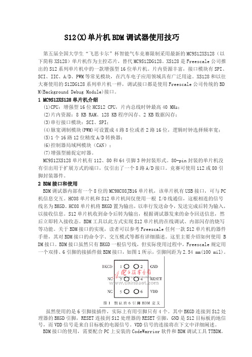
2 BDM接口和使用BDM调试器内部有一个8位的MC9HC08JB16单片机,该单片机有USB接口,可与PC 机信息交互。
HC08单片机和S12单片机间仅使用一根 I/O线通信,这根相连的信号线名为BKGD。
HC08单片机将BKGD置为输出,以串行发送命令,发送完成后转为输入,以接收信息。
S12单片机收到命令后转为输出,根据调试器发来的命令回送信息,然后立即转入接收态。
BDM工具以此方式实现S12单片机的在线调试、内部闪存的烧写等功能。
关于BDM接口的实现,读者可以参考Freescale任何一款S12单片机的器件手册,其对BDM接口的命令字、交互模式等都有详细描述。
Freescale-HCS12和HCS12X-系列单片机简介

前言
目前世界上的单片机或者微控制器的种类繁 多,单片机供应商也有很多,例如Freescale、 ATMEL、NXP、ST、Microchip、Infineon、TI、 NEC等,其中Freescale(飞思卡尔)公司的8位、 16位和32位单片机性能稳定、品种齐全,针对不 同的应用领域可以选择不同性能、型号的单片机。
MC9S12XS单片机原理 及嵌入式系统开发
《MC9S12XS单片机原理及嵌入式系统开发》
第2章 Freescale HCS12和HCS12X
系列单片机简介
HCS12系列单片机概述 HCS12X系列单片机概述 MC9S12XS128简介 CPU12(X)核 MC9S12XS128的存储器映射 MC9S12XS128内部锁相环模块PLL
① 表示质量认定状态。MC表示完全合格产品,XC表示初始产品,PC表示预测试产品。 ② 表示存储器类型。无表示片内带ROM或者片内没有程序存储器,7表示片内带EPROM 或一次可编程ROM(OTP ROM),8表示片内带EEPROM,9表示片内带Flash存储器。 ③ 表示内核类型。S12表示16位单片机,S08表示8位单片机。 ④ 表示系列。DG表示为D系列产品。 ⑤ 表示存储空间大小及版本。128表示128 KB的Flash存储空间,B为Flash版本。 ⑥ 表示工作温度范围。无表示工作温度范围是0℃~70℃,C表示工作温度范围是
《MC9S12XS单片机原理及嵌入式系统开发》
本章着重介绍Freescale公司的HCS12系列 16位单片机的概况,并和HCS12X系列16位双核 单片机进行简单比较,最后给出HCS12系列单片 机最小系统中各部分的设计方案。
《MC9S12XS单片机原理及嵌入式系统开发》
FreeScale HCS12系列单片机教程(dg128)

HCS12微控制器系列教程---第一讲:PWM 模块介绍该教程以MC9S12DG128单片机为核心进行讲解,全面阐释该16位单片机资源。
本文为第一讲,开始介绍S12 MCU的PWM模块。
PWM 调制波有8 个输出通道,每一个输出通道都可以独立的进行输出。
每一个输出通道都有一个精确的计数器(计算脉冲的个数),一个周期控制寄存器和两个可供选择的时钟源。
每一个PWM 输出通道都能调制出占空比从0—100% 变化的波形。
PWM 的主要特点有:1、它有8 个独立的输出通道,并且通过编程可控制其输出波形的周期。
2、每一个输出通道都有一个精确的计数器。
3、每一个通道的PWM 输出使能都可以由编程来控制。
4、PWM输出波形的翻转控制可以通过编程来实现。
5、周期和脉宽可以被双缓冲。
当通道关闭或PWM计数器为0时,改变周期和脉宽才起作用。
6、8 字节或16 字节的通道协议。
7、有4 个时钟源可供选择(A、SA、B、SB),他们提供了一个宽范围的时钟频率。
8、通过编程可以实现希望的时钟周期。
9、具有遇到紧急情况关闭程序的功能。
10、每一个通道都可以通过编程实现左对齐输出还是居中对齐输出。
HCS12微控制器系列教程---第二讲:PWM 寄存器简介1、PWM启动寄存器PWMEPWME 寄存器每一位如图1所示:复位默认值:0000 0000B图1 PWME 寄存器每一个PWM 的输出通道都有一个使能位PWMEx 。
它相当于一个开关,用来启动和关闭相应通道的PWM 波形输出。
当任意的PWMEx 位置1,则相关的PWM输出通道就立刻可用。
用法:PWME7=1 --- 通道7 可对外输出波形PWME7=0 --- 通道7 不能对外输出波形注意:在通道使能后所输出的第一个波形可能是不规则的。
当输出通道工作在串联模式时(PWMCTL寄存器中的CONxx置1),那么)使能相应的16位PWM 输出通道是由PWMEx的高位控制的,例如:设置PWMCTL_CON01 = 1,通道0、1级联,形成一个16位PWM 通道,由通道 1 的使能位控制PWM 的输出。
- 1、下载文档前请自行甄别文档内容的完整性,平台不提供额外的编辑、内容补充、找答案等附加服务。
- 2、"仅部分预览"的文档,不可在线预览部分如存在完整性等问题,可反馈申请退款(可完整预览的文档不适用该条件!)。
- 3、如文档侵犯您的权益,请联系客服反馈,我们会尽快为您处理(人工客服工作时间:9:00-18:30)。
TM
10
How to change default behavior locally
Remember that any memory model allows accesses to banked code or data, It is only the default behavior that changes ! The keywords __far and __near specify the calling convention for functions. Far function calls can “cross” pages. Near function calls must stay in the same page. How to override the calling convention of a function ? using keywords __near and __far ! In the SMALL memory model, functions are near, data is near. In the BANKED memory model functions are far, data is near. In the LARGE memory model functions and data are far by default.
TM
8
Banked Memory Model
Freescale and the Freescale logo are trademarks of Freescale Semiconductor, Inc. All other product or service names are the property of their respective owners. Freescale Semiconductor, Inc. 2006.
TM
12
Overriding default access to variables
__near and __far keywords can also be applied to variable declarations : char __near variable; A variable declared __near is considered by the compiler to be allocated in the zero page (first 256 bytes of the memory space, address range 0x00 – 0xFF) Accessing variables in the zero page generates less code and executes faster since the address used to access them is only one byte long.
TM
6
Comparison between memory models
Let’s compare the assembly instructions generated by the compiler with the following simple code:
Freescale and the Freescale logo are trademarks of Freescale Semiconductor, Inc. All other product or service names are the property of their respective owners. Freescale Semiconductor, Inc. 2006.
A call to a banked function is more expensive both in codesize and execution time.
Freescale and the Freescale logo are trademarks of Freescale Semiconductor, Inc. All other product or service names are the property of their respective owners. Freescale Semiconductor, Inc. 2006.
Advanced C programming for 16-bit MCUs
Austin, Texas 25-29 September, 2006
TM
Freescale and the Freescale logo are trademarks of Freescale Semiconductor, Inc. All other product or service names are the property of their respective owners. Freescale Semiconductor, Inc. 2006.
Freescale and the Freescale logo are trademarks of Freescale Semiconductor, Inc. All other product or service names are the property of their respective owners. Freescale Semiconductor, Inc. 2006.
1
Introduction
What is this training about ?
TM
Agenda
Memory
Models functions calls by hand
Optimizing Running Running
routines in RAM a function from the Stack
TM
3
Memory Models
Models! Where?
TM
What is a memory model ?
Memory Models
A memory model is a set of rules that changes the default behavior of the compiler. It tells the compiler what instructions to generate when accessing data and calling functions. The Compiler for the 16 bits MCU’s supports three different memory models.
TM
ቤተ መጻሕፍቲ ባይዱ13
__near and __far applied to variables or data
char __far variable; A variable declared __far is considered by the compiler to be allocated in a banked memory segment an has to be accessed through a page switch routine. (Like in the large memory model) In what scenarios would we have banked data ? The only banked internal memory resource is Flash (read-only). Therefore if using only internal resources, only constant data (read-only data) can be paged. The other scenario is where we have external RAM accessed through a paged area.
Freescale and the Freescale logo are trademarks of Freescale Semiconductor, Inc. All other product or service names are the property of their respective owners. Freescale Semiconductor, Inc. 2006.
SMALL ( code and data fit in 64Kb )
Data and functions are accessed by default with 16 bit addresses.
BANKED (code in banked memory)
Data is also accessed with 16 bit addresses, functions are called using banked calls
TM
9
Large Memory Model
Freescale and the Freescale logo are trademarks of Freescale Semiconductor, Inc. All other product or service names are the property of their respective owners. Freescale Semiconductor, Inc. 2006.
TM
5
Memory Models
Differences when calling banked and non-banked functions
If a function is in banked memory, it has to be called differently than a function in non–banked memory. In particular: