A Low Jitter 125-1250MHz Process Independent
Richtek Technology 产品说明书:RT2519 低功耗线性电源
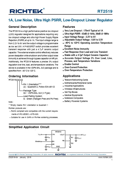
RT2519®Copyright 2018 Richtek Technology Corporation. All rights reserved. is a registered trademark of Richtek Technology Corporation.©1A, Low Noise, Ultra High PSRR, Low-Dropout Linear RegulatorGeneral DescriptionThe RT2519 is a high performance positive low dropout (LDO) regulator designed for applications requiring very low dropout voltage and ultra high Power Supply Ripple Rejection (PSRR) at up to 1A. The input voltage range is from 2.2V to 6V and the output voltage is programmable as low as 0.8V. A P-MOSFET switch provides excellent transient response with just a 4.7μF ceramic output capacitor. The external enable control effectively reduces power dissipation while shutdown and further output noise immunity is achieved through bypass capacitor on NR pin.Additionally, the RT2519 features a precise 3% output regulation over line, load, and temperature variations. The device is available in the VDFN-8AL 3x3 package and is specified from −40°C to 125°C.Features●Very Low Dropout : 170mV Typical at 1A●Ultra High PSRR : 63dB @ 1kHz, 38dB @ 1MHz ●Input Voltage Range : 2.2V to 6V●Adjustable Output Voltage : 0.8V to 5.5V●−40°C to 125°C Operating Junction Temperature Range●Excellent Noise Immunity●Fast Response Over Load and Line Transient ●Stable with a 4.7μF Output Ceramic Capacitor ●Accurate Output Voltage 3% Over Load, Line,Process, and Temperature Variations ●Enable Control●Over-Current Protection●Over-Temperature ProtectionOrdering InformationSimplified Application CircuitApplications●T elecom/Networking Cards ●Motherboards/Peripheral Cards ●Industrial Applications ●Wireless Infrastructures ●Set-Top Boxes●Medical Equipments ●Notebook Computers●Battery Powered SystemsNote :***Empty means Pin1 orientation is Quadrant 1Richtek products are :❝ RoHS compliant and compatible with the current require-ments of IPC/JEDEC J-STD-020.❝ Suitable for use in SnPb or Pb-free soldering processes.VOUTRT2519G : Green (Halogen Free and Pb Free)***RT2519©Copyright 2018 Richtek Technology Corporation. All rights reserved. is a registered trademark of Richtek Technology Corporation.Functional Pin DescriptionFunctional Block DiagramPin Configuration(TOP VIEW)VDFN-8AL 3x3FB KN= : Product CodeYMDNN : Date CodeVOUT FB VOUT GNDVIN VIN ENNRRT2519©Copyright 2018 Richtek Technology Corporation. All rights reserved. is a registered trademark of Richtek Technology Corporation.OperationThe RT2519 is a low noise, high PSRR LDO which supports very low dropout operation. The operating input range from 2.2V to 6V and the output voltage is programmable as low to 0.8V and the output current can be up to 1A. The internal compensation network is well designed to achieve fast transient response with good stability.In steady-state operation, the feedback voltage is regulated to the reference voltage by the internal regulator.When the feedback voltage signal is less than the reference, the output current passes through the power MOSFET will be increased. The extra amount of the current is sent to the output until the voltage level of FB pin returns to the reference.On the other hand, if the feedback voltage is higher than the reference, the power MOSFET current is decreased.The excess charge at the output can be released by the loading current.Start-UpThe RT2519 has a quick-start circuit to charge the noise reduction capacitor (C NR ). The switch of the quick-start circuit is closed at start up.To reduce the noise from bandgap, there is a low-pass (RC) filter consist of the C NR and the resistance which is connected with bandgap, as Functional Block Diagrams present.At the start-up, the quick-start switch is closed, with only 35k Ω resistance between bandgap and NR pin. The quick-start switch opens approximate 2ms after the device is enabled, the resistance between NR and bandgap is about 224k Ω to form a very good low pass filter and with great noise reduction performance.The 35k Ω resistance is used to slow down the reference voltage ramp to avoid inrush current at chip start-up, and the start-up time can be calculated as :t SS (sec) = 160000 x C NR (F) (1)It is recommend the C NR value larger than 0.01μF to reduce noise, and low leakage ceramic capacitors are suitable.However, with too large C NR will extend the start-up time very long if the C NR is not fully charged during 2ms andopens the quick-start switch, the C NR will be chargedthrough higher resistance 224k Ω and takes much longer time to finish the start up process.Enable and Shutdown OperationThe RT2519 goes into sleep mode when the EN pin is in a logic low condition. In this condition, the pass transistor,error amplifier, and bandgap are all turned off, reducing the supply current to only 2μA (max.). If the shutdown mode is not required, the EN pin can be directly tied to VIN pin to keep the LDO on.Current LimitThe RT2519 continuously monitors the output current to protect the pass transistor against abnormal operations.When an overload or short circuit is encountered, the current limit circuitry controls the pass transistor's gate voltage to limit the output within the predefined range. By reason of the build-in body diode, the pass transistor conducts current when the output voltage exceeds input voltage. Since the current is not limited, external current protection should be added if device may work at reverse voltage state.Over-Temperature Protection (OTP)The RT2519 has an over-temperature protection. When the device triggers the OTP , the device shuts down until the temperature back to normal state.Under Voltage Lock-Out (UVLO)The RT2519 utilizes an under voltage lock-out circuit to keep the output shut off until the internal circuitry is operating properly. The UVLO circuit has a de-glitch feature so that it typically ignores undershoot transients on the input if they are less than 30μs duration.RT2519©Copyright 2018 Richtek Technology Corporation. All rights reserved. is a registered trademark of Richtek Technology Corporation.Electrical Characteristics(V IN = V OUT + 0.5V or 2.2V , V OUT = 0.8V and 5.5V, I OUT = 1mA, V EN = 2.2V , C NR = 10nF , C OUT = 4.7μF , T J = −40°C to 125°C, unless otherwise specified)Absolute Maximum Ratings (Note 1)●All Pins ---------------------------------------------------------------------------------------------------------------------- −0.3V to 7V ●Power Dissipation, P D @ T A = 25°CVDFN-8AL 3x3-------------------------------------------------------------------------------------------------------------3.31W●Package Thermal Resistance (Note 2)VDFN-8AL 3x3, θJA --------------------------------------------------------------------------------------------------------30.2°C/W VDFN-8AL 3x3, θJC -------------------------------------------------------------------------------------------------------5.5°C/W ●Lead Temperature (Soldering, 10 sec.)-------------------------------------------------------------------------------260°C ●Junction T emperature -----------------------------------------------------------------------------------------------------150°C●Storage T emperature Range -------------------------------------------------------------------------------------------- −65°C to 150°C ●ESD Susceptibility (Note 3)HBM (Human Body Model)----------------------------------------------------------------------------------------------2kV CDM (Charged Device Model)------------------------------------------------------------------------------------------1kVRecommended Operating Conditions (Note 4)●Supply Voltage, VIN ------------------------------------------------------------------------------------------------------2.2V to 6V●Junction T emperature Range -------------------------------------------------------------------------------------------- −40°C to 125°CRT2519Copyright 2018 Richtek Technology Corporation. All rights reserved. is a registered trademark of Richtek Technology Corporation.RT2519©Copyright 2018 Richtek Technology Corporation. All rights reserved. is a registered trademark of Richtek Technology Corporation.Typical Application CircuitNote 1. Stresses beyond those listed “Absolute Maximum Ratings ” may cause permanent damage to the device. These arestress ratings only, and functional operation of the device at these or any other conditions beyond those indicated in the operational sections of the specifications is not implied. Exposure to absolute maximum rating conditions may affect device reliability.Note 2. θJA is measured under natural convection (still air) at T A = 25°C with the component mounted on a high effective-thermal-conductivity four-layer test board on a JEDEC 51-7 thermal measurement standard. θJC is measured at the exposed pad of the package.Note 3. Devices are ESD sensitive. Handling precaution is recommended.Note 4. The device is not guaranteed to function outside its operating conditions.Note 5. The spec. doesn't cover the tolerances from external resistors, and which is not tested at condition of V OUT = 0.8V, 4.5V≤ V IN ≤ 6V, and 750mA ≤ I OUT ≤ 1A since the power dissipation of the device is totally higher than the maximum rating of the package to lead a thermal shutdown issue.Note : All input and output capacitance in the suggested parameter mean the effective capacitance. The effectivecapacitance needs to consider any De-rating Effect like DC bias.V OUTRT2519©Copyright 2018 Richtek Technology Corporation. All rights reserved. is a registered trademark of Richtek Technology Corporation.Typical Operating Characteristics0.00.51.01.52.02.5-50-25255075100125Temperature (°C)S h u t d o w n C u r r e n t (μA )Reference Voltage vs. Temperature0.7900.7950.8000.8050.810-50-25255075100125Temperature (°C)R e f e r e n c e V o l t a g e (V )UVLO vs. Temperature1.51.61.71.81.92.02.12.2-50-25255075100125Temperature (°C)U V L O (V )PSRR vs. Frequency10203040506070809010 100 1k10k100k1M10MFrequency (Hz)P S R R (d B )Dropout Voltage vs. Output Current0501001502002004006008001000Output Current (mA)D r o p o u t V o l t a g e (m V )Dropout Voltage vs. Input Voltage05010015020023456Input Voltage (V)D r o p o u t V o l t a g e (m V )RT2519©Copyright 2018 Richtek Technology Corporation. All rights reserved. is a registered trademark of Richtek Technology Corporation.Time (50μs/Div)Power Off from ENV OUT (1V/Div)V EN (2V/Div)I OUT(500mA/Div)V IN = 4.3V, V OUT = 3.3VTime (500μs/Div)Power On from ENV OUT (1V/Div)V EN (2V/Div)I OUT(500mA/Div)V IN = 4.3V, V OUT = 3.3VTime (50μs/Div)Load Transient ResponseV OUT (50mV/Div)I OUT(500mA/Div)V IN = 4.3V, V OUT = 3.3V,I OUT = 0.1A to 1A (1A/μs, only shows the transient component)Time (50μs/Div)Line Transient Response V OUT (5mV/Div)V IN (1V/Div)V IN = 3.8V to 4.8V, V OUT = 3.3V,I OUT = 0.1AOutput Spectral Noise Density0.010.101.0010.00100.0010100100010000100000Frequency (Hz)O u t p u t S p e c t r a l N o i s e D e n s i t y (μV /√H z )RT2519©Copyright 2018 Richtek Technology Corporation. All rights reserved. is a registered trademark of Richtek Technology Corporation.Application InformationThe RT2519 is a low voltage, low dropout linear regulator with input voltage from 2.2V to 6V and a fixed output voltage from 0.8V to 5.5V.Dropout VoltageThe dropout voltage refers to the voltage difference between the VIN and VOUT pins while operating at specific output current. The dropout voltage V DO also can be expressed as the voltage drop on the pass-FET at specific output current(I RATED ) while the pass-FET is fully operating at ohmic region and the pass-FET can be characterized as an resistance R DS(ON). Thus the dropout voltage can be defined as (V DO = V VIN − V VOUT = R DS(ON) x I RATED ).For normal operation, the suggested LDO operating range is (V VIN > V VOUT + V DO ) for good transient response and PSRR ability. Vice versa, while operating at the ohmic region will degrade these performance severely.Output Voltage SettingFor the RT2519, the voltage on the FB pin sets the output voltage and is determined by the values of R1 and R2.The values of R1 and R2 can be calculated for any voltage using the formula given in Equation :()OUT R1 + R2V =0.8R2⨯Using lower values for R1 and R2 is recommended to reduces the noise injected from the FB pin. Note that R1is connected from VOUT pin to FB pin, and R2 is connected from FB to GND.Chip Enable OperationThe EN pin is the chip enable input. Pull the EN pin low (<0.4V) will shutdown the device. During shutdown mode,the RT2519 quiescent current drops to lower than 2μA.Drive the EN pin to high (>1.2V, <6V) will turn on the device again. For external timing control (e.g.RC), the EN pin can also be externally pulled to High by adding a 100k Ωor greater resistor from the VIN pin.Current LimitThe RT2519 continuously monitors the output current to protect the pass transistor against abnormal operations.When an overload or short circuit is encountered, thecurrent limit circuitry controls the pass transistor's gatevoltage to limit the output within the predefined range. By reason of the build-in body diode, the pass transistor conducts current when the output voltage exceeds input voltage. Since the current is not limited, external current protection should be added if device may work at reverse voltage state.C IN and C OUT SelectionLike any low dropout regulator, the external capacitors of the RT2519 must be carefully selected for regulator stability and performance. Using a capacitor of at least 4.7μF is suitable. The input capacitor must be located at a distance of no more than 0.5 inch from the input pin of the chip.Any good quality ceramic capacitor can be used. However,a capacitor with larger value and lower ESR (Equivalent Series Resistance) is recommended since it will provide better PSRR and line transient response.The RT2519 is designed specifically to work with low ESR ceramic output capacitor for space saving and performance consideration. Using a ceramic capacitor with capacitance of at least 4.7μF on the RT2519 output ensures stability.Output NoiseGenerally speaking, the dominant noise source is from the internal bandgap for most LDOs. With the noise reduction capacitor connecting to the NR pin of the RT2519, the noise component contributed from bandgap will not be significantly. Instead, the most noise source comes from the output resistor divider and the error amplifier input. For general application to minimize noise,using a 0.01μF noise-reduction capacitor (C NR ) is recommended.Thermal ConsiderationsThermal protection limits power dissipation in the RT2519.When the operation junction temperature exceeds 160°C,the OTP circuit starts the thermal shutdown function and turns the pass element off. The pass element turns on again after the junction temperature cools down by 20°C.The RT2519 output voltage will be closed to zero when output short circuit occurs as shown in Figure 1. It canRT2519©Copyright 2018 Richtek Technology Corporation. All rights reserved. is a registered trademark of Richtek Technology Corporation.reduce the chip temperature and provides maximum safety to end users when output short circuit occurs.The junction temperature should never exceed theabsolute maximum junction temperature T J(MAX), listed under Absolute Maximum Ratings, to avoid permanent damage to the device. The maximum allowable power dissipation depends on the thermal resistance of the IC package, the PCB layout, the rate of surrounding airflow,and the difference between the junction and ambient temperatures. The maximum power dissipation can be calculated using the following formula :P D(MAX) = (T J(MAX) − T A ) / θJAwhere T J(MAX) is the maximum junction temperature, T A is the ambient temperature, and θJA is the junction-to-ambient thermal resistance.For continuous operation, the maximum operating junction temperature indicated under Recommended Operating Conditions is 125°C. The junction-to-ambient thermal resistance, θJA , is highly package dependent. For a VDFN-8AL 3x3 package, the thermal resistance, θJA , is 30.2°C/W on a standard JEDEC 51-7 high effective-thermal-conductivity four-layer test board. The maximum power dissipation at T A = 25°C can be calculated as below :P D(MAX) = (125°C − 25°C) / (30.2°C/W) = 3.31W for a VDFN-8AL 3x3 package.The maximum power dissipation depends on the operating ambient temperature for the fixed T J(MAX) and the thermal resistance, θJA . The derating curves in Figure 2 allowsFigure 1. Short-Circuit Protection when Output Short-Circuit Occurs V OUT Short to GNDV OUTI OUTthe designer to see the effect of rising ambient temperature on the maximum power dissipation.Figure 2. Derating Curve of Maximum Power Dissipation0.00.81.62.43.24.00255075100125Ambient Temperature (°C)M a x i m u m P o w e r D i s s i p a t i o n (W )RT251911DS2519-04 January 2018©Copyright 2018 Richtek Technology Corporation. All rights reserved. is a registered trademark of Richtek Technology yout ConsiderationFigure 3. PCB Layout Guide12DS2519-04 January 2018 Richtek Technology Corporation14F, No. 8, Tai Yuen 1st Street, Chupei City Hsinchu, Taiwan, R.O.C.Tel: (8863)5526789Richtek products are sold by description only. Customers should obtain the latest relevant information and data sheets before placing orders and should verify that such information is current and complete. Richtek cannot assume responsibility for use of any circuitry other than circuitry entirely embodied in a Richtek product. Information furnished by Richtek is believed to be accurate and reliable. However, no responsibility is assumed by Richtek or its subsidiaries for its use;nor for any infringements of patents or other rights of third parties which may result from its use. No license is granted by implication or otherwise under any patent or patent rights of Richtek or its subsidiaries.V-Type 8AL DFN 3x3 Package。
DS91M125 125 MHz 1 4 M-LVDS Repeater with LVDS Inp
DS91M125 125 MHz 1:4 M-LVDS Repeater withLVDS Input Evaluation KitUSER MANUALPart Number: DS91M125EVK NOPBFor the latest documents concerning these products and evaluation kit, visit . Schematics andgerber files are also available at OverviewThe purpose of this document is to familiarize you with the DS91M125 evaluation board, suggest the test setup procedures and instrumentation, and to guide you through some typical measurements that will demonstrate the performance of the device. The board enables the user to examine performance and all functions of theDS91M125 as a standalone device.The DS91M125 is a high-speed 1:4 M-LVDS repeater with an LVDS input designed for multipoint applications with multiple drivers or receivers. The device conforms to TIA/EIA-899 standard. It utilizes M-LVDS technology for low power, high-speed and superior noise immunity.DescriptionFigure 1 below represents the top layer drawing of the board with the silkscreen annotations. It is a 2.5 x 3 inch 4 layer printed circuit board (PCB) that features a single DS91M125 (U2) device.Figure 1 -DS91M125EVK Top View DrawingDS91M125 Evaluation in a Point-to-Point LinkThe following is a recommended procedure for using and evaluating the DS91M125EVK. Figure 2 depicts a typical setup and instrumentation used.1. Select a single DS91M125 evaluation board.2. Apply the power to the board (3.3 V typical) between J3 and J4 power tabs, observe the value of I CC,and compare it with the expected value (refer to the datasheet) to ensure that the devices arefunctional.3. Enable one of the U2 driver outputs. This is accomplished by setting the DE0-3 pin to VDD (JP3-6).4. Connect a signal source to the driver input (DI+, DI-). The signal needs to be an LVDS/M-LVDS/CML/LVPECL compliant signal. Refer to the DS91M125 datasheet for the receiver inputcompatibility.5. Connect one of the U2 outputs (A0-3/B0-3) to an oscilloscope and observe the waveforms.Figure 2 – DS91M125 Test SetupFigure 3 shows an eye diagram acquired at the output of the DS91M125 driver loaded with a 100-ohm resistor. The generator connected to the driver input simulated a 100 Mbps PRBS-7 NRZ.Figure 3 – DS91M125 OutputIMPORTANT NOTICETexas Instruments Incorporated and its subsidiaries(TI)reserve the right to make corrections,modifications,enhancements,improvements, and other changes to its products and services at any time and to discontinue any product or service without notice.Customers should obtain the latest relevant information before placing orders and should verify that such information is current and complete.All products are sold subject to TI’s terms and conditions of sale supplied at the time of order acknowledgment.TI warrants performance of its hardware products to the specifications applicable at the time of sale in accordance with TI’s standard warranty.Testing and other quality control techniques are used to the extent TI deems necessary to support this warranty.Except where mandated by government requirements,testing of all parameters of each product is not necessarily performed.TI assumes no liability for applications assistance or customer product design.Customers are responsible for their products and applications using TI components.To minimize the risks associated with customer products and applications,customers should provide adequate design and operating safeguards.TI does not warrant or represent that any license,either express or implied,is granted under any TI patent right,copyright,mask work right, or other TI intellectual property right relating to any combination,machine,or process in which TI products or services are rmation published by TI regarding third-party products or services does not constitute a license from TI to use such products or services or a warranty or endorsement e of such information may require a license from a third party under the patents or other intellectual property of the third party,or a license from TI under the patents or other intellectual property of TI.Reproduction of TI information in TI data books or data sheets is permissible only if reproduction is without alteration and is accompanied by all associated warranties,conditions,limitations,and notices.Reproduction of this information with alteration is an unfair and deceptive business practice.TI is not responsible or liable for such altered rmation of third parties may be subject to additional restrictions.Resale of TI products or services with statements different from or beyond the parameters stated by TI for that product or service voids all express and any implied warranties for the associated TI product or service and is an unfair and deceptive business practice.TI is not responsible or liable for any such statements.TI products are not authorized for use in safety-critical applications(such as life support)where a failure of the TI product would reasonably be expected to cause severe personal injury or death,unless officers of the parties have executed an agreement specifically governing such use.Buyers represent that they have all necessary expertise in the safety and regulatory ramifications of their applications,and acknowledge and agree that they are solely responsible for all legal,regulatory and safety-related requirements concerning their products and any use of TI products in such safety-critical applications,notwithstanding any applications-related information or support that may be provided by TI.Further,Buyers must fully indemnify TI and its representatives against any damages arising out of the use of TI products in such safety-critical applications.TI products are neither designed nor intended for use in military/aerospace applications or environments unless the TI products are specifically designated by TI as military-grade or"enhanced plastic."Only products designated by TI as military-grade meet military specifications.Buyers acknowledge and agree that any such use of TI products which TI has not designated as military-grade is solely at the Buyer's risk,and that they are solely responsible for compliance with all legal and regulatory requirements in connection with such use. TI products are neither designed nor intended for use in automotive applications or environments unless the specific TI products are designated by TI as compliant with ISO/TS16949requirements.Buyers acknowledge and agree that,if they use any non-designated products in automotive applications,TI will not be responsible for any failure to meet such requirements.Following are URLs where you can obtain information on other Texas Instruments products and application solutions:Products ApplicationsAudio /audio Automotive and Transportation /automotiveAmplifiers Communications and Telecom /communicationsData Converters Computers and Peripherals /computersDLP®Products Consumer Electronics /consumer-appsDSP Energy and Lighting /energyClocks and Timers /clocks Industrial /industrialInterface Medical /medicalLogic Security /securityPower Mgmt Space,Avionics and Defense /space-avionics-defense Microcontrollers Video and Imaging /videoRFID OMAP Mobile Processors /omapWireless Connectivity /wirelessconnectivityTI E2E Community Home Page Mailing Address:Texas Instruments,Post Office Box655303,Dallas,Texas75265Copyright©2012,Texas Instruments Incorporated。
ISL8009A资料
Ordering Information
Applications
• DC/DC POL Modules • µC/µP, FPGA and DSP Power • Plug-in DC/DC Modules for Routers and Switchers • Portable Instruments • Test and Measurement Systems
NOTES: 1. θJA is measured in free air with the component mounted on a high effective thermal conductivity test board with “direct attach” features. See Tech Brief TB379. 2. For θJC, the “case temp” location is the center of the exposed metal pad on the package underside. 3. Limits established by characterization and are not production tested.
The ISL8009A offers a 2ms Power-On-Reset (POR) timer at power-up. The timer output can be reset by RSI. When shutdown, ISL8009A discharges the output capacitor through a 100Ω resistor. Other features include internal digital soft-start, enable for power sequence, overcurrent protection, and thermal shutdown.
MPL3115A2
ORDERING INFORMATION
# of Ports Case No.
None Single Dual
2153
•
Pressure Type Gauge Differential Absolute
•
Digital Interface
•
This document contains information on a new product. Specifications and information herein are subject to change without notice.
Sensors Freescale Semiconductor
MPL3115A2 3
2 Mechanical and Electrical Specifications
2.1 Mechanical Characteristics
Table 1. Mechanical Characteristics @ VDD = 2.5V, T = 25°C unless otherwise noted(1)
Ref Symbol
Parameter
Test Conditions
Min
Pressure Sensor
1
PFS Measurement Range
Calibrated Range
50
Operational Raading Noise
1x Oversample(2) 128x Oversample(2)
Freescale Semiconductor Data Sheet: Advance Information
Document Number: MPL3115A2 Rev 0, 06/2011
THC63LVD827 Datasheet

IOVCC
G7
Power Power Supply Pin for IO inputs circuitry.
LVDSVCC
C5,D3
Power Power Supply Pins for LVDS Outputs.
PLLVCC
C7
Power Power Supply Pin for PLL circuitry.
The 2nd Link. LVDS OUT
The 2nd pixel output data when Dual out.
LVDS OUT LVDS Clock Out for 2nd Link.
IN
Pixel Data Inputs.
IN
Data Enable Input.
IN
Vsync Input.
1. Single in / Dual LVDS out
2. Single in / Single LVDS out
3. Double edge Single in / Dual LVDS out
• 2 LVDS data mapping to simplify PCB layout • Power down mode • Input clock triggering edge selectable by R/F pin • 6bit / 8bit modes selectable by 6B/8B pin
2/18
香港灏业科技 联系人:陈伟 手机:13510979382 QQ:744926516 地址:深圳市南山区高新南六道7B
THC63LVD827_Rev.1.00_E
Pin ription
Pin Name TA1+, TA1TB1+, TB1TC1+, TC1TD1+, TD1TCLK1+, TCLK1TA2+, TA2TB2+, TB2TC2+, TC2TD2+, TD2TCLK2+, TCLK2-
SI5367A-B-GQ资料
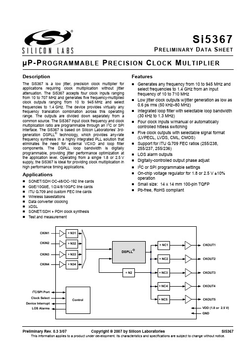
Preliminary Rev. 0.3 3/07Copyright © 2007 by Silicon Laboratories Si5367This information applies to a product under development. Its characteristics and specifications are subject to change without notice.Si5367µP-P R O G R A M M A B L E P R E C I S I O N C L O C K M U L T I P L I E RDescriptionThe Si5367 is a low jitter, precision clock multiplier for applications requiring clock multiplication without jitter attenuation. The Si5367 accepts four clock inputs ranging from 10 to 707MHz and generates five frequency-multiplied clock outputs ranging from 10 to 945MHz and select frequencies to 1.4GHz. The device provides virtually any frequency translation combination across this operating range. The outputs are divided down separately from a common source. The Si5367 input clock frequency and clock multiplication ratio are programmable through an I 2C or SPI interface. The Si5367 is based on Silicon Laboratories' 3rd-generation DSPLL ® technology, which provides any-rate frequency synthesis in a highly integrated PLL solution that eliminates the need for external VCXO and loop filter components. The DSPLL loop bandwidth is digitally programmable, providing jitter performance optimization at the application level. Operating from a single 1.8 or 2.5V supply, the Si5367 is ideal for providing clock multiplication in high performance timing applications.ApplicationsSONET/SDH OC-48/OC-192 line cards GbE/10GbE, 1/2/4/8/10GFC line cards ITU G.709 and custom FEC line cards Wireless basestations Data converter clocking xDSLSONET/SDH + PDH clock synthesisTest and measurementFeaturesGenerates any frequency from 10 to 945MHz and select frequencies to 1.4GHz from an input frequency of 10 to 710MHzLow jitter clock outputs w/jitter generation as low as 0.6ps rms (50 kHz–80 MHz)Integrated loop filter with selectable loop bandwidth (30 kHz to 1.3 MHz)Four clock inputs w/manual or automatically controlled hitless switchingFive clock outputs with selectable signal format (LVPECL, LVDS, CML, CMOS)Support for ITU G.709 FEC ratios (255/238, 255/237, 255/236) LOS alarm outputsDigitally-controlled output phase adjustI 2C or SPI programmable settingsOn-chip voltage regulator for 1.8 or 2.5V ±10% operationSmall size: 14x 14mm 100-pin TQFP Pb-free, RoHS compliantP R E L I M I N A R Y D A TA S H E E TSi53672Preliminary Rev. 0.3Table 1. Performance Specifications(V DD=1.8 or 2.5V ±10%, T A=–40 to 85 ºC)Parameter Symbol Test Condition Min Typ Max Unit Temperature Range T A–402585ºC Supply Voltage V DD 2.25 2.5 2.75V1.62 1.8 1.98V Supply Current I DD f OUT = 622.08 MHzAll CKOUTs enabledLVPECL format output—394435mAOnly CKOUT1 enabled—253284mAf OUT = 19.44 MHzAll CKOUTs enabledCMOS format output—278321mAOnly CKOUT1 enabled—229261mATristate/Sleep Mode—TBD TBD mAInput Clock Frequency (CKIN1, CKIN2, CKIN3, CKIN4)CK F Input frequency and clockmultiplication ratio determinedby programming device PLLdividers. Consult Silicon Labo-ratories configuration softwareDSPLL sim or Any-Rate Preci-sion Clock Family ReferenceManual at /tim-ing to determine PLL dividersettings for a given input fre-quency/clock multiplicationratio combination.10—707.35MHzOutput Clock Frequency (CKOUT1, CKOUT2, CKOUT3, CKOUT4, CKOUT5)CK OF109701213———94511341417MHzInput Clocks (CKIN1, CKIN2, CKIN3, CKIN4)Differential Voltage Swing CKN DPP0.25— 1.9V PP Common Mode Voltage CKN VCM 1.8V ±10%0.9— 1.4V2.5V ±10% 1.0— 1.7V Rise/Fall Time CKN TRF20–80%——11ns Duty Cycle CKN DC Whichever is less40—60%50—ns Output Clocks (CKOUT1, CKOUT2, CKOUT3, CKOUT4, CKOUT5)Common Mode V OCM LVPECL100Ω loadline-to-line V DD–1.42—V DD–1.25VDifferential Output Swing V OD 1.1— 1.9V Single Ended OutputSwingV SE0.5—0.93VNote: For a more comprehensive listing of device specifications, please consult the Silicon Laboratories Any-Rate Precision Clock Family Reference Manual. This document can be downloaded from /timing.Si5367Preliminary Rev. 0.33Rise/Fall Time CKO TRF 20–80%230350ps Duty Cycle CKO DC 45—55%PLL Performance Jitter GenerationJ GENf OUT = 622.08 MHz,LVPECL output format 50kHz–80MHz —0.6TBD ps rms12kHz–20MHz —0.6TBD ps rms 800Hz–80MHz—TBD TBD ps rms Jitter Transfer J PK —0.050.1dB Phase NoiseCKO PNf OUT = 622.08 MHz 100 Hz offset—TBD TBD dBc/Hz 1 kHz offset —TBD TBD dBc/Hz 10 kHz offset —TBD TBD dBc/Hz 100 kHz offset —TBD TBD dBc/Hz 1 MHz offset—TBD TBD dBc/Hz Subharmonic Noise SP SUBH Phase Noise @ 100kHz Offset —TBD TBD dBc Spurious Noise SP SPURMax spur @ n x F3(n > 1, n x F3 < 100MHz)—TBDTBDdBcPackageThermal Resistance Junction to AmbientθJAStill Air —40—ºC/WTable 2. Absolute Maximum RatingsParameterSymbol Value Unit DC Supply Voltage V DD –0.5 to 2.75V LVCMOS Input VoltageV DIG –0.3 to (V DD + 0.3)V Operating Junction Temperature T JCT –55 to 150ºC Storage Temperature RangeT STG–55 to 150ºC ESD HBM Tolerance (100 pF, 1.5k Ω)2kV ESD MM Tolerance 200VLatch-Up ToleranceJESD78 CompliantNote:Permanent device damage may occur if the Absolute Maximum Ratings are exceeded. Functional operation should berestricted to the conditions as specified in the operation sections of this data sheet. Exposure to absolute maximum rating conditions for extended periods of time may affect device reliability.Table 1. Performance Specifications (Continued)(V DD =1.8 or 2.5V ±10%, T A =–40 to 85 ºC)ParameterSymbol Test ConditionMin Typ Max Unit Note: For a more comprehensive listing of device specifications, please consult the Silicon Laboratories Any-Rate PrecisionClock Family Reference Manual. This document can be downloaded from /timing .Si53674Preliminary Rev. 0.3Si5367Preliminary Rev. 0.35Figure 2.Si5367 Typical Application Circuit (IC Control Mode)Figure 3.Si5367 Typical Application Circuit (SPI Control Mode)Si53676Preliminary Rev. 0.31. Functional DescriptionThe Si5367 is a low jitter, precision clock multiplier for applications requiring clock multiplication without jitter attenuation. The Si5367 accepts four clock inputs ranging from 10 to 707MHz and generates five frequency-multiplied clock outputs ranging from 10 to 945MHz and select frequencies to 1.4GHz. The device provides virtually any frequency translation combination across this operating range. Independent dividers are available for every input clock and output clock, so the Si5367 can accept input clocks at different frequencies and it can generate output clocks at different frequencies. The Si5367 input clock frequency and clock multiplication ratio are programmable through an I2C or SPI interface. Silicon Laboratories offers a PC-based software utility, DSPLL sim, that can be used to determine the optimum PLL divider settings for a given input frequency/clock multiplication ratio combination that minimizes phase noise and power consumption. This utility can be downloaded from /timing.The Si5367 is based on Silicon Laboratories' 3rd-generation DSPLL® technology, which provides any-rate frequency synthesis in a highly integrated PLL solution that eliminates the need for external VCXO and loop filter components. The Si5367 PLL loop bandwidth is digitally programmable and supports a range from 30kHz to 1.3MHz. The DSPLL sim software utility can be used to calculate valid loop bandwidth settings for a given input clock frequency/clock multiplication ratio. The Si5367 monitors all input clocks for loss-of-signal and provides a LOS alarm when it detects missing pulses on its inputs.In the case when the input clocks enter alarm conditions, the PLL will freeze the DCO output frequency near its last value to maintain operation with an internal state close to the last valid operating state. The Si5367 has five differential clock outputs. The signal format of the clock outputs is programmable to support LVPECL, LVDS, CML, or CMOS loads. If not required, unused clock outputs can be powered down to minimize power consumption. The phase difference between the selected input clock and the output clocks is adjustable in 200ps increments for system skew control. In addition, the phase of each output clock may be adjusted in relation to the other output clocks. The resolution varies from 800ps to 2.2ns depending on the PLL divider settings. Consult the DSPLL sim configuration software to determine the phase offset resolution for a given input clock/clock multiplication ratio combination. For system-level debugging, a bypass mode is available which drives the output clock directly from the input clock, bypassing the internal DSPLL. The device is powered by a single 1.8 or 2.5V supply.1.1. Further DocumentationConsult the Silicon Laboratories Any-Rate Precision Clock Family Reference Manual (FRM) for more detailed information about the Si5367. The FRM can be downloaded from /timing.Silicon Laboratories has developed a PC-based software utility called DSPLL sim to simplify device configuration, including frequency planning and loop bandwidth selection. This utility can be downloaded from /timing.Si5367Preliminary Rev. 0.372. Pin Descriptions: Si5367Table 3. Si5367 Pin DescriptionsPin #Pin NameI/OSignal LevelDescription1, 2, 4, 17, 20, 22, 23, 24, 25, 37, 47, 48, 49, 50, 51, 52, 53, 54, 55, 56, 66, 67, 72, 73, 74, 75, 80, 85, 95NCNo Connect.These pins must be left unconnected for normal opera-tion.3RST I LVCMOSExternal Reset.Active low input that performs external hardware reset of device. Resets all internal logic to a known state and forces the device registers to their default value. Clock outputs are tristated during reset. After rising edge of RST signal, the device will perform an internal self-cali-bration.This pin has a weak pull-up.Note:Internal register names are indicated by underlined italics, e.g. INT_PIN . See Si5368 Register Map.Si53678Preliminary Rev. 0.35, 6, 15, 27, 32, 42, 62, 63, 76, 79, 81, 84, 86, 89, 91, 94, 96,99, 100V DDVddSupplyV DD .The device operates from a 1.8 or 2.5V supply. Bypass capacitors should be associated with the following V DD pins:Pins Bypass Cap 5, 60.1 µF 150.1 µF 270.1 µF 62, 630.1 µF 76, 79 1.0 µF 81, 840.1 µF 86, 890.1 µF 91, 940.1 µF 96, 99, 1000.1 µF 7, 8, 14, 16, 18, 19, 21, 26, 28, 31, 33, 36, 38, 41, 43, 46, 64,65GND GND SupplyGround.This pin must be connected to system ground. Minimize the ground path impedance for optimal performance.9C1B O LVCMOSCKIN1 Invalid Indicator.This pin performs the CK1_BAD function ifCK1_BAD_PIN =1 and is tristated if CK1_BAD_PIN =0. Active polarity is controlled by CK_BAD_POL .0=No alarm on CKIN1.1=Alarm on CKIN1.10C2B O LVCMOSCKIN2 Invalid Indicator.This pin performs the CK2_BAD function ifCK2_BAD_PIN =1 and is tristated if CK2_BAD_PIN =0. Active polarity is controlled by CK_BAD_POL .0=No alarm on CKIN2.1=Alarm on CKIN2.11C3B O LVCMOSCKIN3 Invalid Indicator.This pin performs the CK3_BAD function ifCK3_BAD_PIN =1 and is tristated if CK3_BAD_PIN =0. Active polarity is controlled by CK_BAD_POL .0=No alarm on CKIN3.1=Alarm on CKIN3.Table 3. Si5367 Pin Descriptions (Continued)Pin #Pin Name I/O Signal Level DescriptionNote:Internal register names are indicated by underlined italics, e.g. INT_PIN . See Si5368 Register Map.Si5367Preliminary Rev. 0.3912INT_ALMOLVCMOSInterrupt/Alarm Output Indicator.This pin functions as a maskable interrupt output with active polarity controlled by the INT_POL register bit. The INT output function can be turned off by setting INT_PIN =0. If the ALRMOUT function is desired instead on this pin, set ALRMOUT_PIN =1 and INT_PIN =0.0=ALRMOUT not active.1=ALRMOUT active.The active polarity is controlled by CK_BAD_POL . If no function is selected, the pin tristates.1357CS0_C3A CS1_C4AI/O LVCMOSInput Clock Select/CKIN3 or CKIN4 Active Clock Indi-cator.If manual clock selection is chosen, and ifCKSEL_PIN =1, the CKSEL pins control clock selection and the CKSEL_REG bits are ignored.If CKSEL_PIN =0,the CKSEL_REG register bits control this function and these inputs tristate. If these pins are not functioning as the CS[1:0] inputs and auto clock selection is enabled, then they serve as the CKIN_n active clock indicator.0=CKIN3 (CKIN4) is not the active input clock1=CKIN3 (CKIN4) is currently the active input to the PLLThe CKn_ACTV_REG bit always reflects the active clock status for CKIN_n. If CKn_ACTV_PIN =1, this status will also be reflected on the CnA pin with active polarity con-trolled by the CK_ACTV_POL bit. IfCKn_ACTV_PIN =0, this output tristates.This pin has a weak pull-down.2930CKIN4+CKIN4–IMULTIClock Input 4.Differential clock input. This input can also be driven with a single-ended signal. CKIN4 serves as the frame sync input associated with the CKIN2 clock when CK_CONFIG_REG =1.3435CKIN2+CKIN2–I MULTIClock Input 2.Differential input clock. This input can also be driven with a single-ended signal.Table 3. Si5367 Pin Descriptions (Continued)Pin #Pin Name I/O Signal Level DescriptionNote:Internal register names are indicated by underlined italics, e.g. INT_PIN . See Si5368 Register Map.CS[1:0]Active Input Clock00CKIN101CKIN210CKIN311CKIN4Si536710Preliminary Rev. 0.33940CKIN3+CKIN3–I MULTI Clock Input 3.Differential clock input. This input can also be driven witha single-ended signal. CKIN3 serves as the frame syncinput associated with the CKIN1 clock whenCK_CONFIG_REG=1.4445CKIN1+CKIN1–I MULTI Clock Input 1.Differential clock input. This input can also be driven witha single-ended signal.58C1A O LVCMOS CKIN1 Active Clock Indicator.This pin serves as the CKIN1 active clock indicator. TheCK1_ACTV_REG bit always reflects the active clock sta-tus for CKIN1. If CK1_ACTV_PIN=1, this status willalso be reflected on the C1A pin with active polarity con-trolled by the CK_ACTV_POL bit. IfCK1_ACTV_PIN=0, this output tristates.59C2A O LVCMOS CKIN2 Active Clock Indicator.This pin serves as the CKIN2 active clock indicator. TheCK2_ACTV_REG bit always reflects the active clock sta-tus for CKIN_2. If CK2_ACTV_PIN=1, this status willalso be reflected on the C2A pin with active polarity con-trolled by the CK_ACTV_POL bit. IfCK2_ACTV_PIN=0, this output tristates.60SCL I LVCMOS Serial Clock.This pin functions as the serial port clock input for bothSPI and I2C modes.This pin has a weak pull-down.61SDA_SDO I/O LVCMOS Serial Data.In I2C microprocessor control mode (CMODE=0), thispin functions as the bidirectional serial data port.In SPImicroprocessor control mode (CMODE=1), this pinfunctions as the serial data output.6869A0A1I LVCMOS Serial Port Address.In I2C control mode (CMODE=0), these pins function ashardware controlled address bits.In SPI control mode (CMODE=1), these pins areignored.This pin has a weak pull-down.70A2_SS I LVCMOS Serial Port Address/Slave Select.In I2C microprocessor control mode (CMODE=0), thispin functions as a hardware controlled address bit.In SPI microprocessor control mode (CMODE=1), thispin functions as the slave select input.This pin has a weak pull-down.Table 3. Si5367 Pin Descriptions (Continued)Pin #Pin Name I/O Signal Level DescriptionNote:Internal register names are indicated by underlined italics, e.g. INT_PIN. See Si5368 Register Map.71SDIILVCMOSSerial Data In.In SPI microprocessor control mode (CMODE =1), this pin functions as the serial data input.In I 2C microprocessor control mode (CMODE =0), this pin is ignored.This pin has a weak pull-down.7778CKOUT3+ CKOUT3–O MULTIClock Output 3.Differential clock output. Output signal format is selected by SFOUT3_REG register bits. Output is differential for LVPECL, LVDS, and CML compatible modes. For CMOS format, both output pins drive identical single-ended clock outputs.8283CKOUT1–CKOUT1+O MULTIClock Output 1.Differential clock output. Output signal format is selected by SFOUT1_REG register bits. Output is differential for LVPECL, LVDS, and CML compatible modes. For CMOS format, both output pins drive identical single-ended clock outputs.8788CKOUT5–CKOUT5+O MULTIClock Output 5.Differential clock output. Output signal format is selected by SFOUT5_REG register bits. Output is differential for LVPECL, LVDS, and CML compatible modes. For CMOS format, both output pins drive identical single-ended clock outputs.90CMODE I 3-LevelControl Mode.Selects I 2C or SPI control mode for the device.0=I 2C Control Mode.1=SPI Control Mode.9293CKOUT2+CKOUT2–O MULTIClock Output 2.Differential clock output. Output signal format is selected by SFOUT2_REG register bits. Output is differential for LVPECL, LVDS, and CML compatible modes. For CMOS format, both output pins drive identical single-ended clock outputs.9798CKOUT4–CKOUT4+O MULTIClock Output 4.Differential clock output. Output signal format is selected by SFOUT4_REG register bits. Output is differential for LVPECL, LVDS, and CML compatible modes. For CMOS format, both output pins drive identical single-ended clock outputs.GND PAD GND PAD GND SupplyGround Pad.The ground pad must provide a low thermal and electri-cal impedance to a ground plane.Table 3. Si5367 Pin Descriptions (Continued)Pin #Pin Name I/O Signal Level DescriptionNote:Internal register names are indicated by underlined italics, e.g. INT_PIN . See Si5368 Register Map.3. Ordering GuideOrdering Part NumberOutput ClockFrequency RangePackage Temperature RangeSi5367A-B-GQ10–945MHz970–1134MHz1.213–1.417GHz100-Pin 14x14mm TQFP–40 to 85°CSi5367B-B-GQ10–808MHz100-Pin 14x14mm TQFP–40 to 85°C Si5367C-B-GQ10–346MHz100-Pin 14x14mm TQFP–40 to 85°C4. Package Outline: 100-Pin TQFPFigure4 illustrates the package details for the Si5367. Table4 lists the values for the dimensions shown in the illustration.Table 4. 100-Pin Package Diagram DimensionsDimension Min Nom Max Dimension Min Nom Max A—— 1.20E16.00 BSC.A10.05—0.15E114.00 BSC.A20.95 1.00 1.05E2 3.85 4.00 4.15b0.170.220.27L0.450.600.75c0.09—0.20aaa——0.20D16.00 BSC.bbb——0.20D114.00 c——0.08D2 3.85 4.00 4.15ddd——0.08e0.50BSC.θ0º 3.5º7ºNotes:1.All dimensions shown are in millimeters (mm) unless otherwise noted.2. Dimensioning and Tolerancing per ANSI Y14.5M-1994.3. This package outline conforms to JEDEC MS-026, variant AED-HD.4. Recommended card reflow profile is per the JEDEC/IPC J-STD-020C specification for Small BodyComponents.5. Recommended PCB LayoutTable 5. PCB Land Pattern DimensionsDimension MIN MAXe0.50BSC.E15.40 REF.D15.40 REF.E2 3.90 4.10D2 3.90 4.10GE13.90—GD13.90—X—0.30Y 1.50REF.ZE—16.90ZD—16.90R10.15 REFR2— 1.00Notes (General):1.All dimensions shown are in millimeters (mm) unless otherwise noted.2. Dimensioning and Tolerancing is per the ANSI Y14.5M-1994 specification.3. This Land Pattern Design is based on IPC-7351 guidelines.4. All dimensions shown are at Maximum Material Condition (MMC). Least Material Condition(LMC) is calculated based on a Fabrication Allowance of 0.05mm.Notes (Solder Mask Design):1.All metal pads are to be non-solder mask defined (NSMD). Clearance between the soldermask and the metal pad is to be 60 µm minimum, all the way around the pad.Notes (Stencil Design):1. A stainless steel, laser-cut and electro-polished stencil with trapezoidal walls should beused to assure good solder paste release.2. The stencil thickness should be 0.125mm (5 mils).3. The ratio of stencil aperture to land pad size should be 1:1 for the perimeter pads.4. A 4x4 array of 0.80mm square openings on 1.05mm pitch should be used for the centerground pad.Notes (Card Assembly):1. A No-Clean, Type-3 solder paste is recommended.2. The recommended card reflow profile is per the JEDEC/IPC J-STD-020C specification forSmall Body Components.D OCUMENT C HANGE L ISTRevision 0.1 to Revision 0.2Changed LVTTL to LVCMOS in Table2, “Absolute Maximum Ratings,” on page3.Updated “2. Pin Descriptions: Si5367”.Changed FSOUT (pins 87 and 88) to CLKOUT5.Changed FS_ALIGN (pin 21) control pin to GND.Changed pin 16 to ground.Revision 0.2 to Revision 0.3Removed references to latency control, INC, and DEC pins.Updated block diagram on page 1.Added Figure1, “Typical Phase Noise Plot,” on page 4.Updated “2. Pin Descriptions: Si5367”.Changed font of register names to underlined italics.Updated "3. Ordering Guide" on page 12.Added “5. Recommended PCB Layout”.N OTES:C ONTACT I NFORMATIONSilicon Laboratories Inc.400 West Cesar ChavezAustin, TX 78701Tel: 1+(512) 416-8500Fax: 1+(512) 416-9669Toll Free: 1+(877) 444-3032Email: Clockinfo@Internet: The information in this document is believed to be accurate in all respects at the time of publication but is subject to change without notice. Silicon Laboratories assumes no responsibility for errors and omissions, and disclaims responsibility for any consequences resulting from the use of information included herein. Additionally, Silicon Laboratories assumes no responsibility for the functioning of undescribed features or parameters. Silicon Laboratories reserves the right to make changes without further notice. Silicon Laboratories makes no warranty, rep-resentation or guarantee regarding the suitability of its products for any particular purpose, nor does Silicon Laboratories assume any liability arising out of the application or use of any product or circuit, and specifically disclaims any and all liability, including without limitation conse-quential or incidental damages. Silicon Laboratories products are not designed, intended, or authorized for use in applications intended to support or sustain life, or for any other application in which the failure of the Silicon Laboratories product could create a situation where per-sonal injury or death may occur. Should Buyer purchase or use Silicon Laboratories products for any such unintended or unauthorized ap-plication, Buyer shall indemnify and hold Silicon Laboratories harmless against all claims and damages.Silicon Laboratories, Silicon Labs, and DSPLL are trademarks of Silicon Laboratories Inc.Other products or brandnames mentioned herein are trademarks or registered trademarks of their respective holders.。
LTC2485CDD资料
0.1
ppm of
VREF/°C
Total Unadjusted Error Output Noise
5V ≤ VCC ≤ 5.5V, VREF = 2.5V, VIN(CM) = 1.25V (Note 6) 5V ≤ VCC ≤ 5.5V, VREF = 5V, VIN(CM) = 2.5V (Note 6) 2.7V ≤ VCC ≤ 5.5V, VREF = 2.5V, VIN(CM) = 1.25V (Note 6)
Negative Full-Scale Error Negative Full-Scale Error Drift
2.5V ≤ VREF ≤ VCC, GND ≤ IN+ = IN– ≤ VCC 2.5V ≤ VREF ≤ VCC, IN+ = 0.75VREF, IN– = 0.25VREF 2.5V ≤ VREF ≤ VCC, IN+ = 0.75VREF, IN– = 0.25VREF
Lead Free Part Marking: /leadfree/
Consult LTC Marketing for parts specified with wider operating temperature ranges. *The temperature grade is identified by a label on the shipping container.
The LTC2485 includes on-chip temperature sensor and an oscillator. The LTC2485 can be configured through an I2C interface to measure an external signal or internal temperature sensor and reject line frequencies. 50Hz, 60Hz or simultaneous 50Hz/60Hz line frequency rejection can be selected as well as a 2x speed-up mode.
NSi812x高可靠双通道数字隔离器数据手册说明书
C O NF ID EN T IA LNSi8120/NSi8121/NSi8122: High ReliabilityDual-Channel Digital IsolatorsDatasheet (EN) 1.8Product OverviewThe NSi812x devices are high reliability dual-channel digital isolator. The NSi812x device is safety certified by UL1577 support several insulation withstand voltages (3.75kV rms , 5kV rms ), while providing high electromagnetic immunity and low emissions at low power consumption. The data rate of the NSi812x is up to 150Mbps, and the common-mode transient immunity (CMTI) is up to 150kV/us. The NSi812x device provides digital channel direction configuration and the default output level configuration when the input power is lost. Wide supply voltage of the NSi812x device support to connect with most digital interface directly, easy to do the level shift. High system level EMC performance enhance reliability and stability of use. AEC-Q100 (Grade 1) option is provided for all devices.Key Features• Up to 5000V rms Insulation voltage• Date rate: DC to 150Mbps• Power supply voltage: 2.5V to 5.5V • All devices are AEC-Q100 qualified • High CMTI: 150kV/us • Chip level ESD: HBM: ±6kV• High system level EMC performance:Enhanced system level ESD, EFT, Surge immunity• Default output high level or low level option • Isolation barrier life: >60 years• Low power consumption: 1.5mA/ch (1 Mbps) • Low propagation delay: <15ns • Operation temperature: -40℃~125℃ • RoHS-compliant packages:SOIC-8 narrow body SOIC-16 wide bodySafety Regulatory Approvals• UL recognition: up to 5000V rms for 1 minute per UL1577• CQC certification per GB4943.1-2011• CSA component notice 5A • DIN VDE V 0884-11:2017-01Applications• Industrial automation system • Isolated SPI, RS232, RS485• General-purpose multichannel isolation • Motor controlFunctional Block DiagramsC O NF ID EN T IA LIndex1.0 ABSOLUTE MAXIMUM RATINGS .............................................................................................................................. 3 2.0 SPECIFICATIONS ........................................................................................................................................................... 3 2.1. E LECTRICAL CHARACTERISTICS .................................................................................................................................................. 3 2.2. TYPICAL PERFORMANCE CHARACTERISTICS ........................................................................................................................... 7 2.3. P ARAMETER M EASUREMENT I NFORMATION . (8)3.0 HIGH VOLTAGE FEATURE DESCRIPTION (9)3.1. INSULATION AND SAFETY RELATED SPECIFICATIONS (9)3.2. DIN VDE V 0884-11(VDE V 0884-11):2017-01 INSULATION CHARATERISTICS ....................................................................... 9 3.3. R EGULATORY INFORMATION ................................................................................................................................................... 11 4.0 FUNCTION DESCRIPTION ..........................................................................................................................................11 5.0 APPLICATION NOTE ................................................................................................................................................... 12 5.1. PCB L AYOUT ...................................................................................................................................................................... 12 5.2. H IGH SPEED PERFORMANCE ................................................................................................................................................... 12 5.3. T YPICAL S UPPLY C URRENT E QUATIONS ..................................................................................................................................... 13 6.0 PACKAGE INFORMATION ......................................................................................................................................... 13 7.0 TAPE AND REEL INFORMATION ............................................................................................................................. 17 8.0 ORDER INFORMATION .............................................................................................................................................. 20 9.0 REVISION HISTORY . (21)C O NF ID EN T IA L1.0 ABSOLUTE MAXIMUM RATINGSPower Supply Voltage VDD1, VDD2 -0.5 6.5 V Maximum Input Voltage VINA, VINB -0.4 VDD+0.41 V Maximum Output Voltage V OUTA , V OUTB -0.4 VDD+0.41 VMaximum Input/Output Pulse VoltageVINA, VINB, V OUTA , V OUTB-0.8VDD+0.8VPulse width should be less than 100ns, and the duty cycle should be less than 10%Common-Mode Transients CMTI ±150 kV/us Output currentIo -15 15mAMaximum Surge Isolation VoltageV IOSM5.3kVOperating Temperature Topr -40125 ℃Storage Temperature Tstg -40150℃Electrostatic dischargeHBM±6000VCDM±2000V1 The maximum voltage must not exceed 6.5V.2.0 SPECIFICATIONS2.1. ELECTRICAL CHARACTERISTICS(VDD1=2.5V~5.5V, VDD2=2.5V~5.5V, Ta=-40℃ to 125℃. Unless otherwise noted, Typical values are at VDD1 = 5V, VDD2 = 5V, Ta =25℃)Power on ResetVDD POR2.2 V POR threshold as during power-upVDD HYS 0.1 V POR threshold Hysteresis Input ThresholdV IT1.6 V Input Threshold at rising edge V IT_HYS 0.4 V Input Threshold Hysteresis High Level Input Voltage V IH 2 V Low Level Input Voltage V IL 0.8 V High Level Output Voltage V OH VDD-0.3 V I OH ≤ 4mA Low Level Output VoltageV OL0.3VI OL ≤ 4mAC O NF ID EN T IA LOutput Impedance R out 50 ohm Input Pull high or low CurrentI pull 8 15 uA Start Up Time after POR trbs 40 usec Common Mode Transient ImmunityCMTI±100±150kV/us(VDD1=5V± 10%, VDD2=5V± 10%, Ta=-40℃ to 125℃. Unless otherwise noted, Typical values are at VDD1 = 5V, VDD2 = 5V, Ta = 25℃)Supply currentNSi8120 I DD1(Q0) 0.58 0.87 mAAll Input 0V for NSi8120x0 Or All Input at supply for NSi8120x1 I DD2(Q0) 1.18 1.77 mA I DD1(Q1) 2.92 4.38 mA All Input at supply for NSi8120x0 Or All Input 0V for NSi8120x1I DD2(Q1) 1.241.86mAI DD1(1M) 1.71 2.56 mA All Input with 1Mbps, C L =15pFI DD2(1M)1.382.07mAI DD1(10M) 1.78 2.67 mA All Input with 10Mbps, C L =15pF I DD2(10M)3.24.8mA I DD1(100M)2.103.15 mA All Input with 100Mbps, C L =15pFI DD2(100M)21.031.5mANSi8121/ NSi8122 I DD1(Q0) 1.031.55 mA All Input 0V for NSi812xx0 Or All Input at supply for NSi812xx1 I DD2(Q0) 1.00 1.5 mA I DD1(Q1)2.203.3 mA All Input at supply for NSi812xx0Or All Input 0V for NSi812xx1 I DD2(Q1)2.133.2 mA I DD1(1M) 1.72 2.58 mA All Input with 1Mbps, C L =15pFI DD2(1M) 1.68 2.52 mA I DD1(10M) 2.62 3.93 mA All Input with 10Mbps, C L =15pFI DD2(10M) 2.71 4.06 mA I DD1(100M) 11.01 16.5 mA All Input with 100Mbps, C L = 15pF I DD2(100M)12.8 19.2 mA Data RateDR 0 150 MbpsC O NF ID EN T IA LPropagation Delayt PLH 5 8.20 15 ns See Figure 2.7 , C L = 15pF t PHL 5 10.56 15 ns See Figure 2.7, C L = 15pF Pulse Width Distortion |t PHL – t PLH | PWD5.0nsSee Figure 2.7 , C L = 15pFRising Time t r 5.0 ns See Figure 2.7 , C L = 15pF Falling Timet f 5.0 ns See Figure 2.7 , C L = 15pFPeak Eye Diagram Jitter t JIT (PK) 350 ps Channel-to-Channel Delay Skewt SK (c2c) 2.5 nsPart-to-Part Delay Skewt SK (p2p)5.0ns(VDD1=3.3V± 10%, VDD2=3.3V± 10%, Ta=-40℃ to 125℃. Unless otherwise noted, Typical values are at VDD1 = 3.3V, VDD2 = 3.3V, Ta =25℃)Supply currentNSi8120 I DD1(Q0) 0.550.83mA All Input 0V for NSi8120x0 Or All Input at supply for NSi8120x1 I DD2(Q0) 1.12 1.68 mA I DD1(Q1) 2.87 4.3 mA All Input at supply for NSi8120x0 Or All Input 0V for NSi8120x1 I DD2(Q1)1.18 1.77mA I DD1(1M)1.72.55mA All Input with 1Mbps, C L = 15pFI DD2(1M)1.271.91 mA I DD1(10M) 1.732.6 mA All Input with 10Mbps, C L = 15pF I DD2(10M)2.413.6 mA I DD1(100M) 2.05 3.08 mA All Input with 100Mbps, C L = 15pF I DD2(100M)14.0521.08mANSi8121/ NSi8122 I DD1(Q0) 0.98 1.47 mA All Input 0V for NSi812xx0 Or All Input at supply for NSi812xx1 I DD2(Q0) 0.95 1.43 mA I DD1(Q1) 2.14 3.21 mA All Input at supply for NSi812xx0 Or All Input 0V for NSi812xx1 I DD2(Q1) 2.08 3.12 mA I DD1(1M) 1.63 2.45 mA All Input with 1Mbps, C L = 15pFI DD2(1M) 1.59 2.39 mA I (10M)2.223.33mAAll Input with 10Mbps,C O NF I D EN T IA LI DD2(10M) 2.25 3.38 mA C L = 15pFI DD1(100M) 7.57 11.36 mA All Input with 100Mbps, C L = 15pF I DD2(100M)8.5 12.75 mA Data RateDR 0 150 Mbps Minimum Pulse Width PW 5.0 nsPropagation Delayt PLH 5 9.20 15 ns See Figure 2.7 , C L = 15pF t PHL5 10.40 15 ns See Figure 2.7, C L = 15pF Pulse Width Distortion |t PHL – t PLH | PWD5.0nsSee Figure 2.7 , C L = 15pFRising Time t r 5.0 ns See Figure 2.7 , C L = 15pF Falling Timet f5.0 nsSee Figure 2.7 , C L = 15pFPeak Eye Diagram Jitter t JIT (PK) 350psChannel-to-Channel Delay Skewt SK (c2c)2.5nsPart-to-Part Delay Skew t SK (p2p)5.0ns(VDD1=2.5V± 10%, VDD2=2.5V± 10%, Ta=-40℃ to 125℃. Unless otherwise noted, Typical values are at VDD1 = 2.5V, VDD2 = 2.5V, Ta =25℃)Supply currentNSi8120I DD1(Q0) 0.53 0.8 mA All Input 0V for NSi8120x0 Or All Input at supply for NSi8120x1 I DD2(Q0) 1.11.65 mA I DD1(Q1)2.85 4.28 mA All Input at supply for NSi8120x0 Or All Input 0V for NSi8120x1 I DD2(Q1)1.15 1.73 mA I DD1(1M) 1.632.45 mA All Input with 1Mbps, C L = 15pFI DD2(1M) 1.21 1.82 mA I DD1(10M) 1.68 2.52 mA All Input with 10Mbps, C L = 15pFI DD2(10M) 2.05 3.08 mA I DD1(100M) 1.95 2.93 mA All Input with 100Mbps, C L = 15pFI DD2(100M)10.415.6mANSi8121/ NSi8122I DD1(Q0) 0.96 1.44 mA All Input 0V for NSi812xx0 Or All Input at supply for NSi812xx1I (Q0)0.931.395mAF ID EN T IA LI DD1(Q1) 2.11 3.165 mA All Input at supply for NSi812xx0Or All Input 0V for NSi812xx1 I DD2(Q1) 2.05 3.075 mA I DD1(1M) 1.58 2.37 mA All Input with 1Mbps, C L = 15pFI DD2(1M) 1.54 2.31 mA I DD1(10M) 2.02 3.03 mA All Input with 10Mbps, C L = 15pFI DD2(10M) 2.04 3.06 mA I DD1(100M) 6.03 9.045 mA All Input with 100Mbps, C L = 15pF I DD2(100M)6 9 mAData RateDR 0 150 Mbps Minimum Pulse Width PW 5.0 nsPropagation Delayt PLH 5 10 15 nsSee Figure 2.7 , C L = 15pF t PHL5 10 15nsSee Figure 2.7, C L = 15pFPulse Width Distortion |t PHL – t PLH | PWD5.0nsSee Figure 2.7 , C L = 15pFRising Time t r5.0ns See Figure 2.7 , C L = 15pF Falling Timet f5.0 ns See Figure 2.7 , C L = 15pFPeak Eye Diagram Jitter t JIT (PK)350ps Channel-to-Channel Delay Skewt SK (c2c)2.5ns Part-to-Part Delay Skew t SK (p2p)5.0ns2.2. TYPICAL PERFORMANCE CHARACTERISTICSFigure 2.1 NSi8120 VDD1 Supply Current vs Data Rate Figure 2.2 NSi8120 VDD2 Supply Current vs Data RateC OE2.3. PARAMETER MEASUREMENT INFORMATIONC LFigure 2.7 Switching Characteristics Test Circuit and WaveformFigure 2.8 Common-Mode Transient Immunity Test CircuitC O NF ID EN T IA L3.0 HIGH VOLTAGE FEATURE DESCRIPTION3.1. INSULATION AND SAFETY RELATED SPECIFICATIONSMinimum External Air Gap (Clearance)L(I01) 4.0 8.0 mm Shortest terminal-to-terminal distance through air Minimum External Tracking (Creepage)L(I02)4.08.0mmShortest terminal-to-terminal distance across the package surfaceMinimum internal gap DTI 20 um Distance through insulationTrackingResistance(Comparative Tracking Index) CTI>400VDIN EN 60112 (VDE 0303-11); IEC 60112Material GroupⅡ3.2. DIN VDE V 0884-11(VDE V 0884-11):2017-01 INSULATION CHARATERISTICSSOIC-8 SOIC-16 Installation Classification per DIN VDE 0110For Rated Mains Voltage ≤ 150V rms Ⅰto Ⅳ Ⅰto Ⅳ For Rated Mains Voltage ≤ 300V rms Ⅰto Ⅲ Ⅰto Ⅳ For Rated Mains Voltage ≤ 400V rms Ⅰto Ⅲ Ⅰto Ⅳ Climatic Classification10/105/2110/105/21 Pollution Degree per DIN VDE 0110, Table 122Maximum repetitive isolation voltageVIORM 565 849 Vpeak Input to Output Test Voltage, Method B1V IORM × 1.5 = V pd (m) , 100%production test, t ini = t m = 1 sec, partial discharge < 5 pCV pd (m)8471273VpeakInput to Output Test Voltage, Method AAfter Environmental Tests Subgroup 1V IORM × 1.2= V pd (m) , t ini = 60 sec, t m = 10 sec, partial V pd (m)6781018VpeakC O N T IA LAfter Input and /or Safety Test Subgroup 2 and Subgroup 3 V IORM × 1.2= V pd (m) , t ini = 60 sec, t m = 10 sec, partialdischarge < 5 pC V pd (m)6781018VpeakMaximum transient isolation voltage t = 60 sec VIOTM 5300 7000 Vpeak Maximum Surge Isolation VoltageTest method per IEC60065,1.2/50uswaveform, VTEST=VIOSM×1.3VIOSM53845384VpeakIsolation resistance VIO =500V RIO >109 >109 Ω Isolation capacitance f = 1MHzCIO 0.6 0.6pFInput capacitanceCI22pF Total Power Dissipation at 25℃Ps1499 mW Safety input, output, or supply currentθJA = 140 °C/W, V I = 5.5 V, T J = 150 °C, T A = 25 °C Is160mAθJA = 84 °C/W, V I = 5.5 V, T J = 150 °C, T A = 25 °C237 mA Case TemperatureTs150150℃Figure 3.2 NSi8120W/NSi8121W/NSi8122W Thermal Derating Curve, Dependence of Safety Limiting Values with Case Temperature per DIN VDE V 0884-11C O NF ID EN T IA L3.3. REGULATORY INFORMATIONThe NSi8120N/NSi8121N/NSi8122N are approved by the organizations listed in table.UL 1577 Component Recognition Program 1Approved under CSA ComponentAcceptance Notice 5ADIN VDE V 0884-11:2017-012Certified by CQC11-471543-2012 GB4943.1-2011Single Protection, 3750V rms Isolation voltageSingle Protection, 3750V rms IsolationvoltageBasic Insulation 565Vpeak, V IOSM =5384VpeakBasic insulation at 400V rms (565Vpeak)File (E500602)File (E500602)File (5024579-4880-0001)File (pending)1 In accordance with UL 1577, each NSi8120N/NSi8121N/NSi8122N is proof tested by applying an insulation test voltage ≥ 4500 Vrms for 1 sec.2 In accordance with DIN VDE V 0884-11, each NSi8120N/NSi8121N/NSi8122N is proof tested by applying an insulation test voltage ≥ 847 V peak for 1 sec(partial discharge detection limit = 5 pC). The * marking branded on the component designates DIN VDE V 0884-11 approval.The NSi8120W/NSi8121W/NSi8122W are approved by the organizations listed in table.UL 1577 Component Recognition Program 1Approved under CSAComponent Acceptance Notice5ADIN VDE V 0884-11(VDE V 0884-11):2017-012 Certified by CQC11-471543-2012 GB4943.1-2011Single Protection, 5000V rms Isolation voltageSingle Protection, 5000V rmsIsolation voltageBasic Insulation 849Vpeak, V IOSM =5384Vpeak Basic insulation at 800V rms (1131Vpeak) Reinforced insulation at 400V rms (565Vpeak)File (E500602)File (E500602)File (5024579-4880-0001)File (pending)1 In accordance with UL 1577, each NSi8120W/NSi8121W/NSi8122W is proof tested by applying an insulation test voltage ≥ 6000 V rms for 1 sec.2 In accordance with DIN VDE V 0884-11, each NSi8120W/NSi8121W/NSi8122W is proof tested by applying an insulation test voltage ≥ 1273 V peak for 1 sec(partial discharge detection limit = 5 pC). The * marking branded on the component designates DIN VDE V 0884-11 approval.4.0 FUNCTION DESCRIPTIONThe NSi812x is a Dual-channel digital isolator based on a capacitive isolation barrier technique. The digital signal is modulated with RF carrier generated by the internal oscillator at the Transmitter side. Then it is transferred through the capacitive isolation barrier and demodulated at the Receiver side.The NSi812x devices are high reliability dual-channel digital isolator with AEC-Q100 qualified. The NSi812x device is safety certified by UL1577 support several insulation withstand voltages (3.75kV rms , 5kV rms ), while providing high electromagnetic immunity and low emissions at low power consumption. The data rate of the NSi812x is up to 150Mbps, and the common-mode transient immunity (CMTI) is up to 150kV/us. The NSi812x device provides digital channel direction configuration and the default output level configuration when the input power is lost. Wide supply voltage of the NSi812x device support to connect with most digital interface directly, easy to do the level shift. High system level EMC performance enhance reliability and stability of use.The NSi812x has a default output status when VDDIN is unready and VDDOUT is ready as shown in Table 4.1, which helps for diagnosis when power is missing at the transmitter side. The output B follows the same status with the input A within 1us after powering up.C O NF ID EN T IA LCopyright © 2019, NOVOSENSEPage 12 Table 4.1 Output status vs. power statusH Ready Ready H Normal operation.L Ready Ready L XUnreadyReadyL HThe output follows the same status with the input within 60us after input side VDD1 is powered on.X Ready Unready XThe output follows the same status with the input within 60us after output side VDD2 is powered on.5.0 APPLICATION NOTE5.1. PCB LAYOUTThe NSi812x requires a 0.1 µF bypass capacitor between VDD1 and GND1, VDD2 and GND2. The capacitor should beplaced as close as possible to the package. Figure 5.1 to Figure 5.4 show the recommended PCB layout, make sure the space under the chip should keep free from planes, traces, pads and via. To enhance the robustness of a design, the user may also include resistors (50–300 Ω ) in series with the inputs and outputs if the system is excessively noisy. The series resistors also improve the system reliability such as latch-up immunity.The typical output impedance of an isolator driver channel is approximately 50 Ω, ±40%. When driving loads where transmission line effects will be a factor, output pins should be appropriately terminated with controlled impedance PCB traces.Figure5.1 Recommended PCB Layout — Top Layer Figure5.2 Recommended PCB Layout — Bottom LayerFigure5.3 Recommended PCB Layout — Top Layer Figure5.4 Recommended PCB Layout — Bottom Layer5.2. HIGH SPEED PERFORMANCEFigure 5.5 shows the eye diagram of NSi812x at 200Mbps data rate output. The result shows a typical measurement on the NSi812x with 350ps p-p jitter.C O NF ID EN T IA LFigure5.5 NSi812x Eye Diagram5.3. TYPICAL SUPPLY CURRENT EQUATIONSThe typical supply current of NSi812x can be calculated using below equations. I DD1 and I DD2 are typical supply currents measured in mA, f is data rate measured in Mbps, C L is the capacitive load measured in pFNSi8120:I DD1 = 0.19 *a1+1.45*b1+0.82*c1. I DD2 = 1.36+ VDD1*f* C L *c1*10-9When a1 is the channel number of low input at side 1, b1 is the channel number of high input at side 1, c1 is the channel number of switch signal input at side 1.NSi8121/ NSi8122:I DD1 = 0.87 +1.26*b1+0.63*c1+ VDD1*f* C L *c2*10-9I DD2 = 0.87 +1.26*b2+0.63*c2+ VDD1*f* C L *c1*10-9When b1 is the channel number of high input at side 1, c1 is the channel number of switch signal input at side 1, b2 is the channel number of high input at side 2, c2 is the channel number of switch signal input at side 2.6.0 PACKAGE INFORMATIONVDD GND 22VDD INA GND 2VDD 2Figure 6.1 NSi8120N Package Figure 6.2 NSi8121N PackageC O NF ID EN T IA LVDD INBGND 22Figure 6.3 NSi8122N PackageFigure 6.4 SOIC8 Package Shape and Dimension in millimeters (inches)Table6.1 NSi8120N/ NSi8121N/ NSi8122N Pin Configuration and DescriptionNSi8121N PIN NO.NSi8122N PIN NO.SYMBOL FUNCTION1 1 1 VDD1 Power Supply for Isolator Side 12 7 2 INA Logic Input A3 3 6 INB Logic Input B4 4 4 GND1 Ground 1, the ground reference for Isolator Side 15 5 5 GND2 Ground 2, the ground reference for Isolator Side 26 6 3 OUTB Logic Output B7 2 7 OUTA Logic Output A888VDD2Power Supply for Isolator Side 2C O NFVDD GND GND 2VDD 2GND 2GND NC NCNC VDD GND GND 2VDD 22GND NC NC NCFigure 6.5 NSi8120W Package Figure 6.6 NSi8121W PackageVDD INB GND GND 2VDD 2GND 2GND NC NC NCFigure 6.7 NSi8122W PackageFigure 6.8 WB SOIC16 Package Shape and Dimension in millimeters and (inches)C O NF ID EN T IA LTable 6.2 NSi8120W/ NSi8121W/ NSi8122W Pin Configuration and Description1 1 1 GND1 Ground 1, the ground reference for Isolator Side 12 2 2 NC No Connection.3 3 3 VDD1 Power Supply for Isolator Side 14 13 4 INA Logic Input A5 5 12 INB Logic Input B6 6 6 NC No Connection.7 7 7 GND1 Ground 1, the ground reference for Isolator Side 18 8 8 NC No Connection. 9 9 9 GND2 Ground 2, the ground reference for Isolator Side 210 10 10 NC No Connection. 11 11 11 NC No Connection. 12 12 5OUTB Logic Output A 13 4 13OUTALogic Output B 14 14 14 VDD2 Power Supply for Isolator Side 215 15 15 NC No Connection.161616GND2Ground 2, the ground reference for Isolator Side 27.0TAPE AND REEL INFORMATIONLAITNEDIFNOCC O NF ID EN T IA LFigure 7.1 Tape and Reel Information of SOIC8LAITNEDIFNOCFigure 7.2 Tape and Reel Information of WB SOIC16NF ID EN T IA L8.0 ORDER INFORMATIONNSi8120N0 3.75 2 0 150 Low -40 to 125℃ NO SOIC8 NSi8120N1 3.75 2 0 150 High -40 to 125℃ NO SOIC8 NSi8121N0 3.75 1 1 150 Low -40 to 125℃ NO SOIC8 NSi8121N1 3.75 1 1 150 High -40 to 125℃ NO SOIC8 NSi8122N0 3.75 1 1 150 Low -40 to 125℃ NO SOIC8 NSi8122N1 3.75 1 1 150 High -40 to 125℃ NO SOIC8 NSi8120W0 5 2 0 150 Low -40 to 125℃ NO WB SOIC16 NSi8120W1 5 2 0 150 High -40 to 125℃ NO WB SOIC16 NSi8121W0 5 1 1 150 Low -40 to 125℃ NO WB SOIC16 NSi8121W1 5 1 1 150 High -40 to 125℃ NO WB SOIC16 NSi8122W0 5 1 1 150 Low -40 to 125℃ NO WB SOIC16 NSi8122W1 5 1 1 150 High -40 to 125℃ NO WB SOIC16 NSi8120N0Q 3.75 2 0 150 Low -40 to 125℃ YES SOIC8 NSi8120N1Q 3.75 2 0 150 High -40 to 125℃ YES SOIC8 NSi8121N0Q 3.75 1 1 150 Low -40 to 125℃ YES SOIC8 NSi8121N1Q 3.75 1 1 150 High -40 to 125℃ YES SOIC8 NSi8122N0Q 3.75 1 1 150 Low -40 to 125℃ YES SOIC8 NSi8122N1Q 3.75 1 1 150 High -40 to 125℃ YES SOIC8 NSi8120W0Q 5 2 0 150 Low -40 to 125℃ YES WB SOIC16 NSi8120W1Q 5 2 0 150 High -40 to 125℃ YES WB SOIC16 NSi8121W0Q 5 1 1 150 Low -40 to 125℃ YES WB SOIC16 NSi8121W1Q 5 1 1 150 High -40 to 125℃ YES WB SOIC16 NSi8122W0Q 5 1 1 150 Low -40 to 125℃ YES WB SOIC16 NSi8122W1Q 5 1 1 150 High -40 to 125℃YES WB SOIC16 NOTE: All packages are RoHS-compliant with peak reflow temperatures of 260 °C according to the JEDEC industry standard classifications and peak solder temperatures. All devices are AEC-Q100 qualified.Part Number Rule:NSi(81)(2)(1)(N)(1)(Q)C O NF ID EN T IA LNSi8120/NSi8121/NSi81229.0 REVISION HISTORY1.0 Original2017/11/15 1.1 Change to Ordering information2018/3/26 1.2 Add maximum operation current specification. 2018/6/20 1.3 Change block diagram 2018/7/28 1.4 Correct Table 6.2 Pin No.2018/8/20 1.5 Add specification “Input Pull high or low Current” 2018/9/10 1.6 Add “Maximum Input/Output Pulse Voltage” 2018/10/91.7 Change to Ordering information 2018/12/20 1.8 Change Certification Information2019/06/17。
FPGA可编程逻辑器件芯片XCVU095-2FFVA2104I中文规格书
FMC Connector JTAG BypassWhen an FMC is attached to the VCU108 board, it is automatically added to the JTAG chain through electronically controlled single-pole single-throw (SPST) switches U26 (HPC0) and U132 (HPC1). The SPST switches are in a normally closed state and transition to an open state when the FMC is attached. Switch U26 adds an attached HPC FMC to the FPGAs JTAG chain as determined by the FMC_HPC0_PRSNT_M2C_B signal. Switch U132 adds an attachedHPC FMC to the FPGAs JTAG chain as determined by the FMC_HPC1_PRSNT_M2C_B signal.The JTAG connectivity on the VCU108 board allows a host computer to download bitstreams to the FPGA using the Xilinx tools. In addition, the JTAG connector allows debug tools such as the Vivado serial I/O analyzer or a software debugger to access the FPGA. The Xilinx tools can also program the BPI parallel flash memory.Clock GenerationThe VCU108 evaluation board provides twelve clock sources to the FPGA as listed in Table1-9.Table 1-9:VCU108 Board Clock SourcesClock Name Clock ReferenceDescription DescriptionSystem clock 300 MHz U122/U157Silicon Labs Si5335A 1.8V LVDS any frequency quad clock generator CLK0 drives U157 quad clock buffer. (SYSCLK1_300_P/N and SYSCLK2_300_P/N)System clock 125 MHz U122Silicon Labs Si5335A 1.8V LVDS any frequency quadclock generator CLK1. (CLK_125 MHz)EMC clock 90 MHz U122Silicon Labs Si5335A 1.8V LVCMOS single-ended any frequency quad clock generator CLK2.(FPGA_EMCCLK)System control clock33.333MHz U122Silicon Labs Si5335A 1.8V LVCMOS single-ended any frequency quad clock generator CLK3. (SYSCTLR_CLK)User clock 10MHz-810MHz U32/U104Silicon Labs Si570 3.3V LVDS I2C programmable oscillator, 156.250 MHz default. U32 output Q0 drives U104 quad clock buffer. (USER_SI570_CLOCK_P/N and MGT_SI570_CLOCK1_P/N thruMGT_SI570_CLOCK3_P/N)Jitter attenuated clock U57Silicon Labs Si5328B LVDS precision clock multiplier/jitter attenuator. See Jitter Attenuated Clock (SI5328_OUT1_P and SI5328_OUT1_N).Table 1-10 lists the VCU108 clock sources to FPGA U1 connections.Jitter attenuated clock U57Silicon Labs Si5328B LVDS precision clockmultiplier/jitter attenuator. See Jitter Attenuated Clock (SI5328_OUT2_P and SI5328_OUT2_N).User SMA clockJ34(P), J35(N)User clock input SMAs. See User SMA Clock(USER_SMA_CLOCK_P and USER_SMA_CLOCK_N).Table 1-10:VCU108 Clock Sources to XCVU095 FPGA U1 ConnectionsClock Source Ref. Des. and PinSchematic Net NameI/O StandardFPGA (U1) PinU157.9SYSCLK1_300_P DIFF_SSTL12G31U157.10SYSCLK1_300_N DIFF_SSTL12F31U157.11SYSCLK2_300_P DIFF_SSTL12G22U157.12SYSCLK2_300_N DIFF_SSTL12G21U122.18CLK_125MHZ_P LVDS BC9U122.17CLK_125MHZ_N LVDS BC8U122.14FPGA_EMCCLK (2)LVCMOS18AL20U122.10SYSCTLR_CLK (2)LVCMOS18U111.C7U104.9USER_SI570_CLOCK_P LVDS_25AU23U104.10USER_SI570_CLOCK_N LVDS_25AV23U104.11MGT_SI570_CLOCK1_P NA (2)V38U104.12MGT_SI570_CLOCK1_N NA (2)V39U104.13MGT_SI570_CLOCK2_P NA (2)AF38U104.14MGT_SI570_CLOCK2_N NA (2)AF39U104.15MGT_SI570_CLOCK3_P NA (2)AH38U104.16MGT_SI570_CLOCK3_N NA (2)AH39U57.28SI5328_OUT1_P NA (1)T38U57.29SI5328_OUT1_N NA (1)T39U57.28SI5328_OUT2_P NA (1)AD38U57.29SI5328_OUT2_N NA (1)AD39J34.1USER_SMA_CLOCK_P LVDS AR14J35.1USER_SMA_CLOCK_NLVDSAT14Notes:1.Capacitively coupled, MGT connections I/O standard is not applicable.2.SI570 U32 SI570_OUTPUT_P/N nets are wired to quad clock buffer U104, (1) also applies.Table 1-9:VCU108 Board Clock Sources (Cont’d)Clock NameClock Reference DescriptionDescriptionJ19FMC_HPC0_HA18_N LVDS L13K19FMC_HPC0_HA21_P LVDS M13J21FMC_HPC0_HA22_P LVDS M15K20FMC_HPC0_HA21_N LVDS M12J22FMC_HPC0_HA22_NLVDS L15K22FMC_HPC0_HA23_P LVDS U11J24NC NA NA K23FMC_HPC0_HA23_NLVDS T11J25NC NA NA K25NC NA NA J27NC NA NA K26NC NA NA J28NC NA NA K28NC NA NA J30NC NA NA K29NC NA NA J31NC NA NA K31NC NA NA J33NC NA NA K32NC NA NA J34NC NA NA K34NC NA NA J36NC NA NA K35NC NA NA J37NC NA NA K37NC NA NA J39NCNANAK38NC NA NA K40NCNANATable 1-34:J22 VITA 57.1 FMC HPC0 Connections (Cont’d)J22 FMC HPC0 Pin Schematic Net Name I/O StandardFPGA (U1) Pin J22 FMC HPC0 Pin Schematic Net Name I/O StandardFPGA (U1)Pin。
Vishay 高速电阻产品说明书
ASVMP• Storage Area Networks(SATA, SAS, Fiber Channel)• Passive Optical Networks (EPON, 10G-EPON, GPON, 10G-PON)• Ethernet (1G, 10GBASE-T,/KR/LR/SR, FCoE • PCI Express • Display port• Low Power Consumption for high speed communication • Exceptional Stability Over Temp. at -40 to +85°C, ±15ppm• Extended Automotive Grade Temp. stability at -55 to +125°C, ±25ppm • Available in 50kG Shock Resistance Configuration upon request • MIL-STD-883 shock and vibration compliant • Durable QFN Plastic Compact Packaging • Standby or Disable Tri-state function• Low jitter (Period jitter RMS and Phase jitter RMS)• High power supply noise reduction, -50dBcLow Jitter High Performance Moisture Sensitivity Level – MSL 1Common Key Electrical Specifications – CMOS, LVPECL, LVDS, and HCSL* For 2.3000MHz < F0 < 9.9999MHz, 6-8 weeks lead-time applies Key Electrical Specifications – CMOSFrequency RangeCMOS 2.3000* 170.0000 MHzCMOS3.3000* 170.0000 LVPECL 2.3000* 460.0000 Commercial, Industrial temp. rangeLVDS 2.3000* 460.0000 Commercial, Industrial temp rangeHCSL2.3000*460.0000Commercial, Industrial temp. rangeOperating Temperature -20 +70 °C See optionsC ° 051+ 55-e r u t a r e p m e T e g a r o t S Overall Frequency Stability -50 +50 ppm See options Supply Voltage (Vdd) +2.25 +3.6 Vs m 5 e m i T p u t r a t S Enable Time 20 ns STD (Tri-state)5 ms PD option (Power Down)s n 5 e m i T e l b a s i D Disable Current20 22 mA STD (Tri-state)0.095 PD option (Power Down)Tri-state Function (Standby/Disable) "1" (VIH 0.75*Vdd) or Open: Oscillation "0" (VIL<0.25*Vdd) : Hi ZV 40k pull-up resister embeddedr a e y t s r i F m p p0.5+ 0.5-g n i g A Supply Current (I dd ) 31 35 mA CL=15pF, 125MHz Output Logic Level V OH 0.9*V ddV I=±6mA V OL 0.1*V dd V Rise Time Tr 1.1 2.0 ns CL=15pF 20% to 80%Fall Time Tf1.32.0 ns% 55 54e l c y C y t u D Integrated Phase Jitter (J PH ) 0.30 2 ps 200kHz ~ 20MHz@125MHz 0.38 2 100kHz ~ 20MHz@125MHz 1.70 2 12kHz ~ 20MHz@125MHzPeriod Jitter RMS (J PERs p0.3)PbRoHS/RoHS II compliant7.0 x 5.0 x 0.85mm-20 ~ +70°C -40 ~ +85°C -40 ~ +105°C -55 ~ +125°CKey Electrical Specifications – LVPECLKey Electrical Specifications – LVDS NotesSupply Current (I dd)56.5 58 mA RL=50 Output Logic Level V OH V dd-1.08 V RL=50V OL V dd-1.55 VPeak to Peak Output Swing (V pp) 800 mV Single endedRise Time Tr 250ps RL=50 , CL=0pFFall Time Tf 250l a i t n e r e f f i D%2584e l c y Cy t u DIntegrated Phase Jitter (J PH) 0.25 2ps200kHz ~ 20MHz@156.25MHz0.38 2 100kHz ~ 20MHz@156.25MHz1.70 2 12kHz ~ 20MHz@156.25MHzPeriod Jitter RMS (J PER s p5.2)Notes Supply Current (I dd)29 32 mA RL=100Output Offset Voltage (V OS) 1.125 1.4 V RL=100 differential Delta Offset Voltage (V OS) 50 mVPeak to Peak Output Swing (V pp) 350 mV Single endedRise Time Tr 200ps RL=50 , CL=2pFFall Time Tf 200l a i t n e r e f f i D%2584e l c y Cy t u DIntegrated Phase Jitter (J PH) 0.28 2ps200kHz ~ 20MHz@156.25MHz0.40 2 100kHz ~ 20MHz@156.25MHz1.70 2 12kHz ~ 20MHz@156.25MHzPeriod Jitter RMS (J PER s p5.2)Key Electrical Specifications – HCSLNotes Supply Current (I dd)40 42 mA RL=50Output Logic Level V OH0.725 V RL=50V OL0.1 V Peak to Peak Output Swing (V pp) 750 mV Single endedRise Time Tr 200 400ps RL=50 , CL=2pFFall Time Tf 200 400l a i t n e r e f f i D%2584e l c y Cy t u DIntegrated Phase Jitter (J PH) 0.25 2ps200kHz ~ 20MHz@156.25MHz0.37 2 100kHz ~ 20MHz@156.25MHz1.70 2 12kHz ~ 20MHz@156.25MHzPeriod Jitter RMS (J PER s p5.2)20% to 80% 20% to 80% 20% to 80%Absolute Maximum RatingsSupply Voltage -0.3 +4.0 VInput Voltage -0.3 V dd+0.3 VJunction Temp. +150 °CStorage Temp. -55 +150 °CSoldering Temp. +260 °C 40sec maxESDHBM MM CDM 4,0004001,500VCMOS OUTPUTTest Circuit(Unless specified otherwise: T=25° C, VDD=3.3 V) LVPECL outputTest CircuitASVMPTest CircuitLVDS OUTPUTHCSL OUTPUTASVMPPbRoHS/RoHS II compliantTest Circuit7.0 x 5.0 x 0.85mmASVMPASVMPFunction Tri-state NC GND Output NC (CMOS)Output (LVPECL, LVDS, HCSL)VddNote: Recommend using an approximately 0.01uF bypass capacitor between PIN 6and 3.Center pad: NC / GNDRecommended Land Pattern for CMOSRecommended Land Pattern for LVPECL, LVDS, HCSLPbRoHS/RoHS II compliant7.0 x 5.0 x 0.85mm6413ASVMPTube: 50pcs/tubeUnit orientation in tube:Dimensions: mmPbRoHS/RoHS II compliant7.0 x 5.0 x 0.85mm。
- 1、下载文档前请自行甄别文档内容的完整性,平台不提供额外的编辑、内容补充、找答案等附加服务。
- 2、"仅部分预览"的文档,不可在线预览部分如存在完整性等问题,可反馈申请退款(可完整预览的文档不适用该条件!)。
- 3、如文档侵犯您的权益,请联系客服反馈,我们会尽快为您处理(人工客服工作时间:9:00-18:30)。
25.2 A Low Jitter 125-1250MHz Process Independent0.18µm CMOS PLL Based on a Sample-ResetLoop FilterAdr an Max m, Baker Scott, Ed Schne der, Melv n Hagge, Steve Chacko, Dan StiurcaCrystal - Cirrus Logic Inc. Austin TXIn mixed analog-digital VLSI ICs, the on-chip PLLs operate in a noisy environment with the most noise contributed by the supply and sub-strate. The low-jitter requirements of these PLLs impose high loop bandwidths, which in standard charge-pump architectures necessi-tate a tradeoff in frequency resolution [1, 2]. This low-jitter high-res-olution ripple-pole-less process-independent 0.18µm CMOS PLL is based on a sample-reset loop filter technique. The key feature of this architecture is elimination of phase detector frequency spurs due to the ICO control current spikes during input phase difference. This is accomplished by averaging the charge injected by the proportional path over an entire input update period. As a consequence, the ICO control current has a shape characterized by a staircase of low ampli-tude steps, versus one characterized by narrow high amplitude puls-es, and needs much less filtering for low-jitter operation.Figure 25.2.1 presents the block diagram of the proposed current-mode process-independent PLL. To reduce the jitter due to power sup-ply noise, the analog and digital portions of the PLL are biased off of two different on-chip 1.5V sub-regulators. A low-jitter PLL synthesiz-er requires high bandwidth (B), and therefore a high input-update fre-quency (fupdate >10*B). A simple high-bandwidth low-resolution sample-reset PLL at the input boosts the reference frequency to approximately 1.3GH z for the input divider of the high-resolution, high-bandwidth PLL. The bandwidth of the high-resolution PLL is equal to or less than the bandwidth of the input PLL, to minimize phase noise contributed by the internal oscillator of the input PLL. The phase frequency detector is a standard 7 NAND gate design with dead-zone avoidance [1, 2]. The charge pump uses source switches to minimize clock feedthrough from the noisy digital supply. The inte-gral path of the loop filter consists of a main charge-pump (Ipmp) that integrates the input phase difference on the Cint capacitance for use by the transconductance stage (Mint), which converts this voltage into a current. The proportional path samples the phase difference for each update period on a Czero capacitance by integrating the current from the feed-forward charge-pump (Ipmpz). This voltage is used to provide a constant current during the entire update period, through a process independent gm stage. To avoid introducing an additional pole in the loop due to the integration on Czero, the voltage on it is reset at the end of each update period. The wide frequency range is achieved with a differential ring oscillator [2], controlled by current, to minimize the coupled noise. The M feedback programmable divider uses a dual modulus architecture with a divide by 2 prescaler and a pulse swallower counter. The output of the divider is resynchronized with the ICO clock to minimize the jitter contribution of the divider.A bandgap circuit provides the PLL with two types of bias currents: a temperature and process independent current (Iti) which is digitally calibrated to an external resistor, and a current (Ibg) proportional to the bandgap voltage (Vbg), divided by an internal reference resistance (Rbg). This gives a process independent mechanism to transfer ratios of the bandgap voltage around the IC (V=a*Ibg* Rbg).Figure 25.2.2 presents the simplified schematic of the current-mode loop filter. A process-independent reference transconductance is gen-erated by a differential pair (Mrgm+, Mrgm-) that is tuned to a con-stant gm by a feedback circuit that regulates its tail current. The input of the gm tune loop differential pair is a process independent bandgap voltage, Vbg. An offset current derived from the Iti current is summed into the drains of the differential pair. The resulting transconductance (gm = 1/Rgm ∝Iti/Vbg) is virtually process inde-pendent. The tail current of the reference gm stage is mirrored into several replica gm stages. By controlling the addition of their output currents, a process-independent programmable gm stage is achieved. This gm is used in conjunction with Czero to form the programmable stabilizing zero for the loop. The resulting stabilizing zero (ωz) is set by the ratio of charge-pump currents, times a ratio of resistances and a ratio of capacitances. It has a low process dependence due to Rint and tracks the natural frequency (ωn):where Kico ∝Ibg*Rbg/Ctotal is the ring oscillator gain, and Ctotal is the total capacitance charged and discharged in the ring element. The resulting damping factor (ξ) is virtually process independent, provid-ed that both Ipmp and Ipmpz are of Ibg type, so that Ipmp*Rint is process independent:To keep the variation of the damping factor less than ±30% over the entire output frequency range, the Cint capacitance is programmed in accordance with the PLL feedback divider value (M) and gm*Czero is programmed with reference to the phase detector update frequency. The sampling capacitance (Czero) is realized by two sets of differen-tial capacitors (Czp_even/odd and Czn_even/odd), which are charged in opposite directions by the Ipmpzp/Ipmpzn proportional path charge-pumps. During even update periods the first set is reset and then samples the phase difference, and during odd update periods it is connected to the programmable gm stage to generate the feed-for-ward current. The second set of capacitances operates in complemen-tary fashion.Figure 25.2.3 presents the top level schematic of the current con-trolled, four ring element oscillator. It uses an active load differential inverter [2], which produces a smaller process dispersion in the Kico gain versus other differential inverters. By matching the devices Mrefp/Mrefn and Mlimitp/Mlimitn, the amplitude of oscillation can be made a multiple of the Vbg. This process and supply-voltage-inde-pendent swing further reduce the dispersion of the gain and improve the PSRR. To achieve a wide frequency range with linear control, the ICO current range should be minimized. Therefore the gain of the oscillator is decreased at low output frequencies by connecting addi-tional capacitances (Cgain) at the differential output of the ring ele-ments. The update frequency ripple of the control current due to the dead-zone avoidance pulses is filtered-out by the loop. The high-fre-quency pole seen at the ring element input (gm(Min)/Cpole_intern) eliminates the need for an additional on-chip ripple filtering capaci-tance. The PLL exhibits low-jitter operation with pole-zero separation ωp/ωz=150-300, which increases the phase margin towards 90°, simi-lar to type II second-order PLLs.Figure 25.2.4 presents the differential to single-ended converter that consists of a wide-band diode-load differential input stage followed by a shunt feedback differential pair that performs the conversion. By including an inverter in the shunt feedback of the differential pair that matches the output inverter, the trip point of the differential to single ended converter behaves well over process and temperature, giving a precise 50±0.5% duty-cycle output signal.Figure 25.2.5 presents the PLL transient locking waveforms. The top plot shows the integral and proportional path currents, together with the total ICO control current, while the bottom plot displays the dif-ferential voltage at the input of the process independent gm stage. Figure 25.2.6 shows the process and temperature variation of the ICO frequency-versus-current curves. Gain variation of the oscillator is only ±9% over the worst-case process and temperature corners. The main PLL specifications are: frequency range 125-1250MHz, resolu-tion better than 500kHz, supply voltage 2.5V analog/1.5V digital, jit-ter <0.3%Tosc, and power consumption 75mW.References:[1] J. Maneatis, “Low jitter process independent DLL and PLL based on self-biased techniques”, IEEE JSCC, vol. 31, no. 11, pp. 1723-1732, Nov. 1996. [2] D. Mijuskovic, e. a., “Cell based fully integrated CMOS frequency synthesizer”, IEEE JSSC, vol. 29, no. 3, pp. 271-279, March 1994.Figure 25.2.5: Transient locking waveforms.Figure 25.2.6: ICO frequency-versus-current curves.Figure 25.2.2: Current-mode sample-reset loop filter.Figure 25.2.3: ICO with process independent output amplitude.。