K-SYNC同步器使用说明
同步控制器使用手册

安全须知无论在任何情况下,如操作、清洁或保养,请务必遵守以下所规定的安全守则,若有因违反,而造成超出原设计、制造的安全顾虑,本公司将不予以负责。
当地若另有其它的安全规范,则请一起遵守。
警告:请在本设备允许的操作和储存环境条件下使用。
·任何情况下,无专业人员指导,切勿拆卸或碰触内部零部件;·维修设备时,严禁带电操作;·切勿使金属、液体等异物掉入设备内,以免设备损坏;·设备安装尽量远离干扰源(例如:接触器、变频器等)或采取相应的屏蔽措施;·信号线、电源线最好分开走线,以免产生干扰;·本设备与接触器不可共享一个电源,否则会有干扰产生;·本设备专门为本公司生产的VFD系列变频器配套使用而设计,使之能够发挥最佳性能,但不能保证与其它品牌变频器的匹配。
储存本品在安装之前必须置于其包装箱内,若该机暂不使用,为了使该品能够在本公司的保修范围内以及日后的维护,储存时务必注意下列事项:☞必须置于无尘垢、干燥之位置。
☞储存位置的环境温度必须在0℃到+65℃范围内。
☞储存位置的相对湿度必须在5%到90%范围内,且无结露。
☞避免储存于含有腐蚀性气、液体之环境中。
☞最好适当包装并存放在架子或台面上。
操作环境☞环境温度0℃-+50℃,若环境温度超过40℃以上时,请置于通风良好之场所。
☞相对湿度15%-+95%RH,避免安装与任何发生结露、冰冻或要接触任何液体之场所。
☞不要安装一任何有以下情况的场所:阳光直晒、浓灰尘、腐蚀性气体或油雾、易燃性气体、液体。
☞震动小于5.9米/妙(0.6g)。
SLC系列同步控制器拥有完善的功能,在技术上处于国内领先水平,在性能上可与国外同类产品相媲美。
广泛适用于由多台调速系统组成的各种机械设备上,如电力、钢铁、造纸、纺织、印染、电缆光纤、塑料等行业。
可对线速度、位移、张力、距离等进行控制,是机器设备的最佳选择。
一、型号说明SLC 04C22 (A)B 为反馈电压为0-10VA 为反馈电压为±5V控制器输出路数4路控制器系列号1、主要特点A、数字化SLC04C22A(B)控制器采用单片计算机控制,可对控制器进行多种参数设置,设置参数时通过数码显示。
同步器使用技巧
第二篇:提高篇第六章:同步器使用技巧本书已经介绍过同步器的作用和使用方法,这里详细介绍同步器的使用技巧。
第一节:同步器的应用范围操作同步器可以达到和操作网络表相同的效果,就是通过同步器,把原理图元件对应的封装放置到PCB图里,并且相同的网络用网络线表示连接,根据这些网络线,就可以自动布线或者手工布线。
1、网络表生成的网络名称是顺序编号的网络名称,同步器生成的网络名称是以管脚号为基础的网络名称,这两种不同的网络名称可以达到相同的自动布线或者手工布线效果。
2、引入网络表放置的PCB元件是堆在一起的,还需要弹开元件的操作,降低了绘图速度,用同步器放置的PCB元件是顺序排列的,这就加快了绘图速度。
3、同步器生成网络有两种方法,一种是更新放置,一种是更新添加,下面就以电路图1.sch为例,介绍同步器生成网络的两种方法:更新放置,是指绘制好原理图之后,原理图元件也添加了对应PCB的封装,PCB文件里没有元件,在原理图里执行菜单命令Design设计/Update Pcb更新PCB,弹出更新设计的同步器对话框,用鼠标点Preview Changes按钮,这时候的更新设计的信息如图6-1-1,更新添加是指绘制好原理图之后,原理图元件添加了对应PCB的封装,PCB文件里已经放置了原理图元件对应的PCB 的封装,这时候在原理图里更新PCB会弹出如图6-1-2的元件匹配对话框,用鼠标点Apply(应用)按钮,弹出更新设计的同步器对话框,用鼠标点Execute按钮就可以添加网络。
第二节:同步器的使用原理在原理图方面,只要原理图里有元件,不管这个元件是从元件库管理器里放置的还是直接从库里放置的,或者从别的图纸复制来的,只要原理图元件添加了该元件对应的PCB 正确的封装,就可以进行同步设计了。
在PCB方面,如果是用同步器放置原理图元件对应的PCB封装,这个封装在当前使用的库里必须有这个元件,新自制的元件必须在元件库管理器里看到这个元件,这一点很容易忽视,使得刚自制好的元件一使用同步器就出错,解决的方法很简单,在自制完原理图元件或者PCB元件保存元件之后,回到原理图或PCB图文件,用鼠标点一下自制元件所在的库名称,自制的元件就出现在库管理器里了,这个操作相当于确认新自制的元件。
【2017年整理】英博BKR简单操作说明

英博BKR-12T型补偿控制器简单操作说明⏹菜单界面介绍控制器液晶屏最上部左上角显示目标功率因数值,i代表感性,c代表容性;右上角区显示☺则表示预设正确(功能正确),显示☹则表示有异常,需检查原因。
控制器液晶屏左右两侧垂直四方条显示电容步数,即每路电容投切情况,左侧从上至下是1~6路,右侧从上到下是7~12路,当该路电容投入时对应路会反显(该区域变黑)。
控制器液晶屏中央是控制器菜单、设置、测量值的主显示区,全为英文显示,选择进入相应的菜单会有相应的显示或设定,手动投切、参数设置、测量数值等都能从本区看到。
控制器液晶屏最下部是菜单导航功能符号,▲/▼表示上翻/下翻菜单,►表示进入子菜单,◄表示退出子菜单,◄►表示更改设置,+/-表示增加/减小选定参数值,回车键表示确认或保存值。
⏹菜单设置MEASUREMENT V ALUES---------显示测量值(参数)在液晶屏上简写为“MEAS.V ALUES”;HARMONICS----------显示谐波测量值;STEPINFO--------------显示关于电容器步的信息(每步电容设置参数值);SETUP-------------------显示控制器设置,需密码进入:密码为:2402(升级版本以后的不需密码) DEVICE INFO---------显示控制器信息,如控制器类型、版本等。
如需选择进入控制器设置,通过按▲/▼来翻动主菜单,使左右箭头指中的即 >SETUP<时即为选中SETUP 菜单,再按►即进入该子菜单,会提示输入密码,除了SETUP需要密码,其余菜单不需要输入密码,特别说明:在之后的新版本中,进入SETUP也不需要输入密码,直接进入即可。
◆MEASUREMENT V ALUES测量值:按▲/▼键选择值,测量值会依次显示出来,可显示ULL、ULN、THD OF Voltage、P、Q、S、F、I、等等。
◆HARMONICS谐波值:按◄►键切换不同显示值,按▲/▼键翻动菜单,可依次查看跟谐波有关数值。
键盘鼠标同步器怎么用
键盘鼠标同步器怎么用有许多网友为了工作或者游戏需要,购买了键盘鼠标同步器,但却不知道怎么使用。
没关系,小编在这里为大家详细讲解键盘鼠标同步器的使用方法。
一.简介键盘鼠标同步器主要实现将键盘鼠标信号同步的传输到各个受控的计算机,为了保证数据同步性,以纯硬件的方式将键盘鼠标并行发送到受控的计算机,达到精确的同步效果。
同步器支持PS2键盘鼠标输入,USB信号输出,USB输出接到各个受控计算机,受控计算机可以独立的关机,冷启,热启。
同步器电源直接由计算机提供,同步器在使用时不需要安装任何额外的软件或驱动。
同步器键盘支持连发功能,可以同时设置小于7个连发键。
支持键盘的两种切换功能,通过切换,可以实现控制任意单台或几台计算机。
同步器鼠标支持三种工作模式。
安装方法:请务必按照这个顺序安装开机状态--》必须先连接键鼠到同步器--》最后再连接同步器到电脑二.键盘功能:切换功能一这种方式切换可以实现任一台可控电脑有效,或全部都有效。
切换方法:小键盘上的*按键盘+ 小键盘上的0-6 (以一控六为例) 按住小键盘上的* 键,再按一下小键盘上的 1键,切换到第一台电脑,键盘鼠标只对第一台电脑有效。
按住小键盘上的* 键,再按一下小键盘上的 2键,切换到第一台电脑,键盘鼠标只对第二台电脑有效。
按住小键盘上的* 键,再按一下小键盘上的 3键,切换到第一台电脑,键盘鼠标只对第三台电脑有效。
按住小键盘上的* 键,再按一下小键盘上的 4键,切换到第一台电脑,键盘鼠标只对第四台电脑有效。
按住小键盘上的* 键,再按一下小键盘上的 5键,切换到第一台电脑,键盘鼠标只对第五台电脑有效。
按住小键盘上的* 键,再按一下小键盘上的 6键,切换到第一台电脑,键盘鼠标只对第六台电脑有效。
按住小键盘上的* 键,再按一下小键盘上的0 键,键盘鼠标对所有电脑都有效。
注:切换时可以看对应的指示灯,对应路的指示灯点亮的电脑控制有效。
c. 切换功能二(此功能专门用户才有!)这种方式切换可以实现控制任意接入的多台电脑同步控制,可以配合切换功能一,灵活控制多台电脑同步。
ZL系列Sync网络同步器产品简介说明书
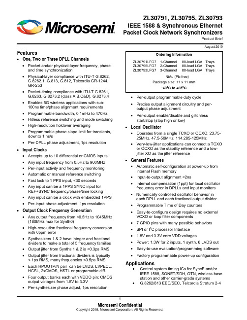
ZL30791, ZL30795, ZL30793IEEE 1588 & Synchronous EthernetPacket Clock Network SynchronizersProduct BriefAugust 2019 Features•One, Two or Three DPLL Channels•Packet and/or physical-layer frequency, phaseand time synchronization•Physical-layer compliance with ITU-T G.8262,G.8262.1, G.813, G.812, Telcordia GR-1244,GR-253•Packet-timing compliance with ITU-T G.8261,G.8263, G.8273.2 (class A,B,C&D), G.8273.4•Enables 5G wireless applications with sub-100ns time/phase alignment requirements •Programmable bandwidth, 0.1mHz to 470Hz•Hitless reference switching and mode switching •High-resolution holdover averaging•Programmable phase slope limit for transients, downto 1 ns/s•Per-DPLL phase adjustment, 1ps resolution•Input Clocks•Accepts up to 10 differential or CMOS inputs•Any input frequency from 0.5Hz to 900MHz•Per-input activity and frequency monitoring•Automatic or manual reference switching•Fast lock to 1 PPS input, <30 seconds•Any input can be a 1PPS SYNC input for REF+SYNC frequency/phase/time locking •Any input can be a clock with embedded 1PPS •Per-input phase adjustment, 1ps resolution•Output Clock Frequency Generation•Any output frequency from <0.5Hz to 1045MHz (180MHz max for Synth0)•High-resolution fractional frequency conversion with 0ppm error•Synthesizers 1 & 2 have integer and fractional dividers to make a total of 5 frequency families •Output jitter from Synths 1 & 2 is <0.3ps RMS •Output jitter from fractional dividers is typically < 1ps RMS, many frequencies <0.5ps RMS •Each HPOUTP/N pair can be LVDS, LVPECL, HCSL, 2xCMOS, HSTL or programable diff.•Four output banks each with VDDO pin; CMOS output voltages from 1.5V to 3.3V•Per-synthesizer phase adjust, 1ps resolution•Per-output programmable duty cycle•Precise output alignment circuitry and per-output phase adjustment•Per-output enable/disable and glitchlessstart/stop (stop high or low)•Local Oscillator•Operates from a single TCXO or OCXO: 23.75-25MHz, 47.5-50MHz, 114.285-125MHz •Very-low-jitter applications can connect a TCXO or OCXO as the stability reference and a low-jitter XO as the jitter reference•General Features•Automatic self-configuration at power-up from internal Flash memory•Input-to-output alignment <2ns•Internal compensation (1ppt) for local oscillator frequency error in DPLLs and input monitors •Numerically controlled oscillator behavior in each DPLL and each fractional output divider •Programmable Time of Day counters•Easy-to-configure design requires no external VCXO or loop filter components•7 GPIO pins with many possible behaviors•SPI or I2C processor Interface• 1.8V and 3.3V core VDD voltages•Power: 1.3W for 2 inputs, 1 synth, 6 LVDS out •Easy-to-use evaluation/programming software •Factory programmable power-up configuration Applications•Central system timing ICs for SyncE and/or IEEE 1588, SONET/SDH, OTN, wireless basestation and other carrier-grade systems •G.8262/813 EEC/SEC, Telcordia Stratum 2-4Ordering InformationZL30791LFG7 1-Channel 80-lead LGA TraysZL30795LFG7 2-Channel 80-lead LGA TraysZL30793LFG7 3-Channel 80-lead LGA TraysNiAu (Pb-free)Package size: 11 x 11 mm-40︒C to +85︒C1. Block DiagramFigure 1 - Functional Block Diagram2. Application ExampleFigure 2 - Synchronous Ethernet and IEEE 1588 Central Timing ApplicationPACKET_REF[2:0]Register A ccessFracDiv IntDiv FracDivIntDivHP Synthesizer 2low-jitterHPOUT6P HPOUT6N HPOUT7P HPOUT7NDIVREF0P DPLL0R S T _BC S _B _A S E L 0S C K _S C LS O _A S E L 1S I _S D AG P I O [8:0]Microprocessor Port SPI or I2C I/F & GPIO Pins One Diff / Two Single-Ended REF0N REF1P One Diff / Two Single-Ended REF1N REF2P One Diff / Two Single-EndedREF2NREF3P One Diff / Two Single-Ended REF3N REF4P One Diff / Two Single-EndedREF4NReference Monitors & State MachinesDPLL1DPLL2HP Synthesizer 1low-jitterGP Synthesizer 0general purpos eGPOUT0GPOUT1DIV DIVXO Optional x2O S C IO S C OMaster Clock M C L K I N _PDIVHPOUT4P HPOUT4N HPOUT5P HPOUT5N DIV DIVHPOUT0P HPOUT0N HPOUT1P HPOUT1N DIVDIV HPOUT2P HPOUT2N HPOUT3P HPOUT3NDIVDIVM C L K I N _NS R S T _BGPS (1PPS)BITS/SSU Line Extracted Clocks[7:0]TCXODPLL0T4 pathSynth01.544 or2.048MHz CMOS to BITS/SSU1 PPSDPLL1SyncESynth12x 156.25MHz 2x 125MHz155.52MHz, 161.1328125MHz or other frequencyDPLL21588Control info from IEEE 1588 algorithmSynth225MHz 1 PPS or clock w/ embedded PPS 1588 signals to system componentsSyncE signals to system componentsto BITS/SSU systemDPLL1 only present on ZL30795 and ZL30793 DPLL2 only present on ZL307933. Detailed Features3.1 Input Block Features•Ten input reference pins; each can accept a CMOS signal or the POS side of a differential pair; or two can be paired to accept both sides of a differential pair•Any input can be a SYNC signal for REF+SYNC frequency/phase/time locking•Any input can be a clock signal with embedded PPS signal (duty cycle distortion indicates PPS location) •Input clocks can be any frequency from 0.5Hz up to 900MHz (180MHz max for CMOS inputs)•Supported telecom frequencies include PDH, SDH, Synchronous Ethernet, OTN, wireless•Inputs constantly monitored by programmable frequency and single-cycle monitors•Single-cycle monitor can quickly disqualify a reference when measured period is incorrect•Frequency measurement (ppb or Hz) and monitoring (coarse, fine, and frequency-step monitors)•Optional input clock invalidation on GPIO assertion to react to LOS signals from PHYs•Input-to-input phase measurement, 1ps resolution•Input-to-DPLL phase measurement, 1ps resolution•Per-input phase adjustment, 1ps resolution3.2 DPLL Features•One, two or three full-featured DPLLs•Very high-resolution DPLL architecture•State machine automatically transitions among freerun, tracking and holdover states•Revertive or nonrevertive reference selection algorithm•Programmable bandwidth from 0.1mHz to 470Hz•Less than 0.1dB gain peaking•Fast frequency/phase/time lock capability for 1PPS or clock+1PPS input references•Programmable phase-slope limiting (PSL)•Programmable frequency rate-of-change limiting (FCL)•Programmable tracking range (i.e. hold-in range)•Truly hitless reference switching and mode switching•Physical-to-physical reference switching•Physical-to-packet reference switching•Packet-to-physical reference switching•Packet-to-packet reference switching•Per-DPLL phase adjustment, 1ps resolution•High-resolution frequency and phase measurement•Fast detection of input clock failure and transition to holdover mode•High-resolution holdover frequency averaging, better than 0.01ppb when using <10mHz filter•Time-of-Day registers: 48-bit seconds, 32-bit nanoseconds, writeable on input PPS edge3.3 Synthesizer Features•Any-to-any frequency conversion with 0ppm error•Two low-jitter synthesizers (Synth1, Synth2) with very high-resolution fractional scaling (i.e. non-integer multiplication)•Two output dividers per low-jitter synthesizer: one integer (4 to 15 plus half divides 4.5 to 7.5) and one 40-bit fractional•One general-purpose synthesizer (Synth0)• A total of five output frequency families•Easy-to-configure, completely encapsulated design requires no external VCXO or loop filter components3.4 Low-Jitter Output Clock Features•Up to 16 single-ended outputs (up to 8 differential outputs) from Synth1 and Synth2•Each output can be one differential output or two CMOS outputs•Output clocks can be any frequency from 1Hz to 1045MHz (250MHz max for CMOS and HSTL outputs)•Output jitter from Synth1 and Synth2 integer dividers is <0.3ps RMS•Output jitter from fractional dividers is <1ps RMS, many frequencies <0.5ps RMS•In CMOS mode, the HPOUTxN frequency can be an integer divisor of the HPOUTxP frequency (Example 1: HPOUT3P 125MHz, HPOUT3N 25MHz. Example 2: HPOUT2P 25MHz, HPOUT2N 1Hz) •Outputs directly interface (DC coupled) with LVDS, LVPECL, HSTL, HCSL and CMOS components •Supported telecom frequencies include PDH, SDH, Synchronous Ethernet, OTN•Can produce clock frequencies for microprocessors, ASICs, FPGAs and other components•Can produce PCIe clocks•Sophisticated output-to-output phase alignment•Per-synthesizer phase adjustment, 1ps resolution•Per-output phase adjustment•Per-output duty cycle / pulse width configuration•Per-output enable/disable•Per-output glitchless start/stop (stop high or low)3.5 General-Purpose Output Clock Features•Two CMOS outputs from Synth0•Any frequency from 0.5Hz to 180MHz•Output jitter is typically 20-30ps•Useful for applications where the component or system receiving the signal has low bandwidth such asa central timing IC•Can output a clock signal with embedded PPS (ePPS) (duty cycle distortion indicates PPS location) 3.6 Local Oscillator•Operates from a single TCXO or OCXO. Acceptable frequencies: 23.75MHz to 25MHz, 47.5MHz to 50MHz, 114.285MHz to 125MHz. Best jitter: ≥48MHz.•Very-low-jitter applications can connect a TCXO or OCXO (any frequency, any output jitter) as the stability reference and a low-cost low-jitter XO as the jitter reference•This ability to have separate jitter and stability references greatly reduces the cost of the TCXO or OCXO (no jitter requirement, no high-frequency-requirement) and allows reuse of already-qualifiedTCXO and OCXO components3.7 General Features•Automatic self-configuration at power-up from internal Flash memory•Input-to-output alignment <200ps with external feedback•Fast REF+SYNC locking for frequency and 1PPS phase alignment with lower-cost oscillator•Generates output SYNC signals: 1PPS (IEEE 1588), 2kHz or 8kHz (SONET/SDH) or other frequency •JESD204B clocking: device clock and SYSREF signal generation with skew adjustment•Internal compensation for local oscillator frequency error in DPLLs and input monitors, 1ppt resolution •Numerically controlled oscillator (NCO) behavior allows system software to steer DPLL frequency or fractional output divider frequency with resolution better than 0.005ppt•Spread-spectrum modulation available in each fractional output divider (PCIe compliant)•Seven general-purpose I/O pins each with many possible status and control options•SPI or I2C serial microprocessor interface3.8 Evaluation Software•Simple, intuitive Windows-based graphical user interface•Supports all device features and register fields•Makes lab evaluation of the device quick and easy•Generates configuration scripts to be stored in internal Flash memory•Generates full or partial configuration scripts to be run on a system processor•Works with or without an evaluation board4. Software FeaturesThe following figure shows the Time Synchronization Algorithm system environment. The subsections below list the features of the Time Synchronization Algorithm.Host ProcessorTransport Layer ProtocolsMicrosemi ZLS30390IEEE 1588-2008Protocol EngineMicrosemi ZLS30380Time Sync AlgorithmMicrosemiPLLSyncE/Stratum 3/GNSS/IEEE 1588Microsemi Ethernet MAC & PHY(Timestamp)Operating SystemApplication LayerControl, Configuration, Stats & AlarmsPacket NetworkClockPPSTimestamp Reference Clock4.1 Time Synchronization AlgorithmThe Time Synchronization Algorithm is responsible to accurately synchronize the local clock to a selected Server. The Time Synchronization Algorithm is synchronizing the Client to the Server to meet a variety of specifications or applications related to frequency accuracy (FFO), frequency (MTIE, TDEV), phase (1 Hz or 1PPS) and time (UTC & GNSS/GPS).The Time Synchronization Algorithm can run on a variety of host processor architectures, whether embedded into an SoC or on a dedicated small scale CPU (such as Microsemi’s SmartFusion2 SoC FP GA). The Time Synchronization Algorithm will interconnect with a wide array of software-programmable clock generators (such as Microsemi’s Network Synchronizer PLLs), protocol engines (such as Microsemi’s ZLS30390 IEEE 1588-2008 Protocol Engine) and underlying Ethernet MACs and PHYs that perform hardware timestamping.4.2 End Application Target PerformanceThe Time Synchronization Algorithm is suitable for many end application targets, including:• Frequency offset accuracy performance for GSM, WCDMA-FDD, LTE-FDD femtocell, small cell (residential, urban, rural, enterprise), picocell and macrocell applications, with target performance less than ± 15 ppb• Frequency performance for ITU-T G.823 and G.824 synchronization interface, as well as G.8261 PNT EEC, PNT PEC and CES interface specifications•Phase Synchronization performance for WCDMA-TDD, Mobile WiMAX, TD-SCDMA, CDMA2000, LTE-TDD, LTE-A, LTE-A Pro and 5G NR femtocell, small cell (residential, urban, rural, enterprise), picocell and macrocell applications with target performance less than ± 1 μs phase alignment •Time Synchronization for TAI, UTC-traceability and GNSS/GPS replacement4.3 Packet NetworksThe Time Synchronization Algorithm is suitable for high performance over a variety of packet networks including:• ITU-T G.8261 Appendix VI• ITU-T G.8261.1 network limit compliant• ITU-T G.8271.1 network limit compliant without SyncE •ITU-T G.8271.2 network limit compliant•Native Ethernet (switched) & IP (routed) networks•xDSL•Microwave•Fully aware, partially aware and unaware timing supported networks•Networks including intermediate Boundary Clocks and Transparent Clocks•Networks with and without SyncE or frequency physical layer support4.4 Clock SpecificationsThe Time Synchronization Algorithm meets the performance requirements from ITU-T packet clock specifications, or draft packet clock specifications, including:•ITU-T G.8261 Appendix VI•ITU-T G.8263 PEC-S•ITU-T G.8273.2 T-BC full on-path without SyncE•ITU-T G.8273.2 T-BC full on-path with SyncE•ITU-T G.8273.2 T-TSC full on-path without SyncE•ITU-T G.8273.2 T-TSC full on-path with SyncE•ITU-T G.8273.4 T-BC-A (draft)•ITU-T G.8273.4 T-BC-P (draft)•ITU-T G.8273.4 T-TSC-A (draft)•ITU-T G.8273.4 T-TSC-P (draft)4.5 ProfilesThe Time Synchronization Algorithm is suitable for use in a wide variety of markets and applications, including the following IEEE 1588-2008 Profiles:•IEEE 1588 Annex J.3 Delay Request-Response Default Profile (2008)•IEEE 1588 Annex J.4 Peer-to-peer Default Profile (2008)•ITU-T G.8265.1 Telecom Profile for Frequency Synchronization (Edition 1)•ITU-T G.8275.1 Telecom Profile for Phase with Full Timing Support Networks (Edition 1)•ITU-T G.8275.1 Telecom Profile for Phase with Full Timing Support Networks (Edition 2)•ITU-T G.8275.2 Telecom Profile for Phase with Partial Timing Support Networks (Edition 1)•CableLabs CM-SP-RDTI Remote DTI Profile (Edition I0x)•AES 67 Standard for Audio Applications of Networks – High-Performance Streaming Audio-over-IP interoperability: PTP Profile for Media Applications•SMPTE 2095-2 Profile for Use of IEEE-1588 Precision Time Protocol in Professional Broadcast Applications•AES R16 Project Report – PTP parameters for AES67 and SMPTE ST 2059-2 interoperability•IEEE C37.238 Standard Profile for Use of IEEE 1588 Precision Time Protocol in Power System Applications (Edition 2011)•IEEE C37.238 Standard Profile for Use of IEEE 1588 Precision Time Protocol in Power System Applications (Edition 2017)•IEC 61850-9-3 Precision time protocol profile for power utility automation (Edition 1.0)•IEC 62439-3 PTP profiles for high-availability automation networks (Edition 3.0)•IEEE802.1as AVB-TSN gPTP•IEEE 1588-2018 Annex J.5 High Accuracy Profile (based on White Rabbit)•IETF TICTOC Enterprise Profile4.6 Monitoring & RedundancyThe Time Synchronization Algorithm includes monitoring and redundancy for high availability synchronization, including:•Synchronization to the best available server•Client monitoring of secondary server referenceso Monitoring includes full time synchronization reporting of secondary servero Supports a programmable number of secondary server connections•Hitless reference switching between multiple servers•Holdover when server packet connectivity is lost•TIE-clear option to build out, or clear, phase offsets between server references4.7 GeneralThe Time Synchronization Algorithm includes many advanced features to aide in the high-accuracy & high-stability applications, including:•Full PLL state machine (Freerun, Holdover, Frequency Lock Acquiring, Frequency Lock Acquired, Phase Lock Acquired), with programmable thresholds for state transitions•Programmable, non-linear packet selection with PDV suppression•Programmable bandwidth configurability from sub-mHz to 100s of mHz.•Programmable packet rates from 1 packet/second to over 128 packets/second•Programmable phase slope limiting, down to 1 ns/s•Programmable frequency change limiting, down to 1 ppb/s•Warm-start to initialize or seed the Time Synchronization Algorithm from a stored or last-known-good frequency offset to improve convergence•Programmable thresholds for management of phase errors: when to adjust with frequency offsets and when to adjust with phase jumps•User ability to manually add frequency offsets due to temperature or ageing (especially during holdover state)4.8 ReportingThe Time Synchronization Algorithm includes user reporting to aide in performance debugging, including: •Set of user notifications about packet network events, such as packet loss, small transient phase jumps, large transient phase jumps, outliers, network path re-routes•Set of metrics related to the synchronization, such as frequency stability and phase stability•Independent reporting of the forward path and reverse path lock status•Oscillator stability analysis for excessive ageing or temperature variation•Server tracking impairments such as pull-in range exceeded4.9 Product Number SupportThere are several Time Synchronization Algorithm products. The following table provides a summary of support with the ZL3079x devices. Refer to ZLS30380 API User Guide section 1.0 “Products”.Product Number Product Name SupportedZLS30387 Basic Frequency and Phase Support NoZLS30384 IntermediateNoFrequency & PhaseSupportZLS30383 QualcommNoSmall Cell CustomZLS30380 Advanced YesMicrosemi Corporate Headquarters One EnterpriseAliso Viejo, CA 92656 USAWithin the USA: +1 (800) 713-4113 Outside the USA: +1 (949) 380-6100 Sales: +1 (949) 380-6136Fax: +1 (949) 215-4996E-mail: ***************************©2019 Microsemi Corporation. All rights reserved. Microsemi and the Microsemi logo are trademarks of Microsemi Corporation. All other trademarks and service marks are the property of their respective owners. Microsemi Corporation (Nasdaq: MSCC) offers a comprehensive portfolio of semiconductor and system solutions for communications, defense & security, aerospace and industrial markets. Products include high-performance and radiation-hardened analog mixed-signal integrated circuits, FPGAs, SoCs and ASICs; power management products; timing and synchronization devices and precise time solutions, setting the world’s standard for time; voice processing devices; RF solutions; discrete components; security technologies and scalable anti-tamper products; Power-over-Ethernet ICs and midspans; as well as custom design capabilities and services. Microsemi is headquartered in Aliso Viejo, Calif., and has approximately 3,400 employees globally. Learn more at .Microsemi makes no warranty, representation, or guarantee regarding the information contained herein or the suitability of its products and services for any particular purpose, nor does Microsemi assume any liability whatsoever arising out of the application or use of any product or circuit. The products sold hereunder and any other products sold by Microsemi have been subject to limited testing and should not be used in conjunction with mission-critical equipment or applications. Any performance specifications are believed to be reliable but are not verified, and Buyer must conduct and complete all performance and other testing of the products, alone and together with, or installed in, any end-products. Buyer shall not rely on any data and performance specifications or parameters provided by Microsemi. It is the Buyer’s responsibility to independently determine suitability of any products and to test and verify the same. The information provided by Microsemi hereunder is provided “as is, where is” and with all faults, and the entire risk associated with such information is entirely with the Buyer. Microsemi does not grant, explicitly or implicitly, to any party any patent rights, licenses, or any other IP rights, whether with regard to such information itself or anything described by such information. Information provided in this document is proprietary to Microsemi, and Microsemi reserves the right to make any changes to the information in this document or to any products and services at any time without notice.。
K-SYNC同步器使用说明

Synchronizing unit
Sync status for each installed echo sounder.
Echo sounders may be disabled
Disabled echo sounders will not be triggered, even if they are member of a group.
SU16 Synchronizing unit
Synchronizing unit
Synchronizing unit
The SU 16 Synchronizing Unit provides highly configurable timing of pinging when multiple echo sounders are employed on a vessel.
Approximate sound speed: Used for travel time calculations.
Synchronizing unit
Settings->Installation->Installation settings
Password: simrad0
To add or remove echo sounders from this list:
Not used 6 5 4 Trig In (CTS/RTT) 3 2 1 Transmitting (input) Trig Out
嵌入式视音频延时器
BD30AV--EB 嵌入式视音频延时器使用说明书B&M CHINA二00三年八月前言恭喜你决定使用BD30AV—EB嵌入式视音频同步延时器,BD30AV—EB嵌入式视音频同步延时器的设计为专业视频用户带来了无法比拟的性能,方便直观的操作,以及可信赖的稳定性。
本手册将会教你安装和使用BD30AV—EB嵌入式视音频同步延时器,并说明了BD30AV—EB嵌入式视音频同步延时器和其它设备的联接方法。
BD30AV—EB嵌入式视音频同步延时器是一个宽频带的具有时基校正和帧同步功能的延时器,它的延时时间可由零到三十秒调整。
BD30AV--EB采用最新芯片设计,指标高、性能好,广泛应用于卫星转播及现场直播等场合。
BD30AV--EB的面板使用 VFD 液晶显示板,使用户更容易精确控制。
BD30AV--EB所有按键选用进口轻触型开关,使用舒适。
BD30AV--EB控制面板一目了然,产品易学易用,在下一部分中,将介绍BD30AV--EB的安装、操作和具体应用。
和所有的BM系列产品一样,BD30AV--EB为你提供多年的保修服务。
本公司保证提供优质的产品设计、生产和售后服务,如有问题和建议,请与我们联系。
安全信息电源本产品使用的电源,不能超过255Vrms(在火线与零线之间或者火线与地线之间)。
电源接地保护对于安全操作十分重要。
接地本产品通过电源线中的地线接地。
为了防止遭到电击,在将本产品接到电源之前,要先将电源线插入正确的插座中。
不接地的危险若没有接地保护,所有产品的部件,包括把手和旋钮,都将是未绝缘的,这样很容易使人遭到电击。
使用环境不要在下列的环境中使用本产品:高温、潮湿、恶劣的气候、未知的电源电压或装有不恰当的保险丝。
产品的外壳和面板为避免受到人身伤害,请不要拿掉产品的外壳或面板。
在没有正确安装外壳和面板之前,请不要操作设备。
产品说明本章对BD30AV—EB嵌入式视音频同步延时器作了基本的概述。
介绍了输入输出视音频连接、电源连接、操作控制和面板 VFD 显示器。
[讲解]轩氏同步器使用说明
![[讲解]轩氏同步器使用说明](https://img.taocdn.com/s3/m/cc9bd3eb900ef12d2af90242a8956bec0975a57e.png)
轩氏同步器使用说明键盘鼠标同步器说明书1.串屏功能:关于同步器串屏功能设置方法:小键盘“*”+S 打开串屏并默认第一台电脑控制有效小键盘“*”+E 或小键盘“*”+0关闭串屏并默认全部电脑控制有效说明:1).单个同步器有串屏功能,多个同步器级联没有串屏功能, 多个设备级联串屏没有意义。
2).在串屏模式下,支持键盘切换功能。
3). 串屏模式下不支持退出同步的切换。
3). 鼠标串屏到某一台电脑后,键盘也在对应的电脑有效。
功能实现:以6台电脑串屏为例:要求可以从左向右串屏1->2->3->4->5->6->1,也可以从右向左串屏6->5->4->3->2->1->6,串屏时,比如由PC1串到PC2,光标从PC1的最右边开始串到PC2的最左边,依次类推。
2.退出功能:同步器在同步控制过程中,可以把指定的电脑退出同步控制退出方法:空格右边的win键(也就是空格右边的窗口键)+小键盘的 1~8键切换方法:按住小键盘 * 组合 1~8键,在8台电脑之间切换按住小键盘 * 组合 0键,8台电脑同步(开机默认同步)鼠标工作模式:1.正常工作模式:(同步器加电默认工作方式)切换方法:按住鼠标左键,中键,右键,松开中键,松开左键和右键进入正常工作模式2.3D模式:切换方法:按住鼠标中键,再按一下鼠标左键,进入3D模式,3D 模式用鼠标移动人物视角时能保持完全同步(此模式有很多技巧,有经验的用户可以尝试)。
3.DN(龙之谷)模式:切换方法:按住鼠标中键,再按一下鼠标右键,进入DN模式。
一、功能介绍1、同步功能:来自同一套键盘鼠标的动作指令通过同步器分出多路完全相同的信号,同步传送给多台电脑,以实现多台电脑的动作完全一致!例如,按“A”则几台显示器上同出现“A”,按“1”则同时出现“1”;鼠标也一样,几台电脑的鼠标箭头以相同的轨迹移动。
2、切换功能(单手切换):通过切换功能可以选择任意一台电脑单独控制。
- 1、下载文档前请自行甄别文档内容的完整性,平台不提供额外的编辑、内容补充、找答案等附加服务。
- 2、"仅部分预览"的文档,不可在线预览部分如存在完整性等问题,可反馈申请退款(可完整预览的文档不适用该条件!)。
- 3、如文档侵犯您的权益,请联系客服反馈,我们会尽快为您处理(人工客服工作时间:9:00-18:30)。
Network interface
Synchronizing unit
External depth for trigger period calculations may be input
Synchronizing unit
The Synchronizing unit provides one output and two inputs for each echo sounder: • Trigger signal (output): tells the echo sounder when to transmit.. • Ready to transmit signal (input): communicates when the echo sounder is ready for the next ping • Transmitting signal (input): tells the Synchronizing Unit when the echo sounder is transmitting.
Synchronizing unit
Software: • Network based SU operator SW may be run on any PC. • System setup • System monitoring When setup, SU will continue to trig the echo sounders if the operator SW is closed.
Synchronizing unit
System setup
To be able to change any installation settings: Press “Allow modification” and input correct password
Synchronizing unit
Synchronizinபைடு நூலகம் unit
The Synchronizing Unit system consists of two main components: • A Workstation PC running the Synchronizing Unit (SU) application. • A Synchronizing Unit that interfaces with the echo sounders.
Synchronizing unit
Inside SU16
One pr echo sounder
O01-
I00 I01 I02 I03 I04 I05
-O15
Synchronizing unit
Inside SU16 cabinet
Main fuse
Synchronizing unit
W249A SU 16 synchronization interface
Approximate sound speed: Used for travel time calculations.
Synchronizing unit
Settings->Installation->Installation settings
Password: simrad0
To add or remove echo sounders from this list:
For each echo sounder to be connected: • • • • Read their manuals and find info: Which output signals are available, Trig, CTS and On/OFF Signal level: TTL or RS232 Impedance
Synchronizing unit
CAUTION! Always power up the Synchronizing Unit before other echo sounders are turned on to avoid accidental pinging. Trigger outputs are undefined during power-up (first 20 seconds) and signal levels could potentially be interpreted as trigger pulse by the echo sounders until signal levels have settled.
Settings->System settings…
Depth datagrams from echo sounder
Sync units‟s IP address and port number
Supported depth datagram formats: • NMEA depth (DBS, input datagram) • NMEA DPT (input datagram) • EAx: Single beam depth (EA 500 input datagram) • EM Depth „D‟: Multibeam depth (e.g. EM 120, EM 1002, EM 3000, EM 3002) • EM Depth „X‟: Multibeam depth (e.g. EM 122, EM 710) • EM Depth „E‟: Single beam depth (e.g. EA 600)
Synchronizing unit
Realtime trigger display
Trigger Transmit and busy Trigger
Ready
Yellow line separates the trigger groups
OS38 is busy much longer than EM 710 and determines the ping rate
Synchronizing unit
Operation: • • • SU controls pinging of each echo sounder. SU receives ready signals from echo sounders, but, if no status signals from echo sounders, SU may estimated ping time period.
Synchronizing unit
How to assign echo sounders to trigger groups
If some echo sounders shall ping several times before next instrument, make many equal groups
Synchronizing unit
Settings->Installation->Installation settings
Mark the echo sounders that are actually connected to the SU. Add new echo sounder if it is not already in the list.
• •
• • • • •
Avoid interference. Schedules the echo sounders transmit times.
16 trigger groups. Groups are triggered consecutively. Any number of echo sounders in a group (zero or more). Echo sounders in a group are triggered simultaneously. Optimizes timing: Transmit duration of each group is dependent on the measured active period for each echo sounder.
Synchronizing unit
Diagnostic tool
Shows signal level and pulses on each input and output signal. (Green = 5v(high)) Module and pin numbers refer to physical connections inside the SU. Terminal ID refer to selections in the installation settings.
Synchronizing unit
System control Push to pause sync.
Synchronizing unit
System status
Incoming depth status Override incoming depth
Depth is available
Synchronizing unit
Is signal active high or low?
Output trigger pulse setup: Check echo sounder manual.
Synchronizing unit
Not used 6 5 4 Trig In (CTS/RTT) 3 2 1 Transmitting (input) Trig Out
Gnd
Synchronizing unit
W249A SU 16 synchronization interface explanation
Synchronizing unit
Which group is active at the moment Empty groups are skipped