同步器设计手册.
新KMD系列平澜同步器新KMD系列说明书综述

KMD系列电机同步控制器使用说明书上海滇驰电子电器有限公司上海平澜电子电器有限公司目录一.型号说明 (2)二.主要特点 (2)三.主要技术指标 (3)四.使用条件 (3)五.面板说明 (4)六.接线端子说明 (5)七.控制器原理框图及功能说明 (6)八.参数码、参数值设定说明 (10)九.参数码、参数值一览表 (10)十.多台同步控制器的联接及注意事项............................................ .12十一.反馈的使用及注意事项............................................................. .13 十二.故障检修与维护 ......................................................................... .14 十三.外形尺寸....................................................................................... .15KMD系列电机同步控制器是本公司在原生产的单一型号基础上推出的成系列电机调速同步控制装置,内部采用计算机为核心的全数字化设计,每台控制器能同时控制四台或八台电机的运转,且使用非常灵活、简便。
KMD系列电机同步控制器拥有强大、完善的功能,在技术上处于国内领先水平,在性能上可与国外同类产品相媲美。
广泛适用于由多台调速系统组成的各种机械设备上,如电力、钢铁、造纸、纺织、印染、电缆光纤、塑料等行业。
可对线速度、位移、张力、距离等进行控制,是电机同步控制的最佳选择。
.型号说明K M D 08_B版本号1---------------- 控制器输出路数(04、08)----------------- 控制器系列号二.主要特点1.数字化KM系列控制器采用单片计算机控制,可通过对控制器进行多种参数设置,设置参数时通过数码显示。
《电动汽车同步器设计与计算案例综述3300字》

电动汽车同步器设计与计算案例综述1.1.同步器选型本设计中,同步器的结构为锁环式,又称为滑块式。
这种同步器的结构主要包括齿毂、滑块、定位销、弹簧、结合齿圈。
考虑到其组合与自身功能,同步器的各个零件有着功能尺寸与配合安装的尺寸。
同步器的每个零件都需要自己的功能尺寸,同时在安装过程中零件之间也要有匹配的尺寸;联接夹具的外径,花键孔的大直径,花键参数和宽度;还有相应的零件尺寸参数同步环,例如同步带孔大端的直径,半锥角,圆锥形表面的长度,摩擦系数,锁紧角度,组合齿的分度环半径,齿端的倒角,边线角度,同步环槽的宽度,刮油器和排油槽的参数;箔的宽度;合适的尺寸包括滑块中的圆形照明同步器环的凹槽,安全行程,接近尺寸,滑块的末端自由度等。
在设计之初,同步器的参数基于为了获得较短的组合时间,良好的驾驶舒适性和较长的使用寿命,已开发了同步器的寿命和组合性能。
1.1是锁紧环同步器的剖视图:图1.11、同步器接合套2、同步环3、同步环4、花键毂5、同步器弹簧6-7、同步器滑块块同步器附件被弹簧固定在一个固定的齿轮插座上(每组3组)。
同步推进单元的头部位于一个环形齿轮槽中。
当传动装置向轴向移动时,首先必须克服同步压力单元的阻力,然后由推进器推进器施加的力必须通过弹簧、传动轴同步和同步同步来达到柔性换向,达到明显的效果。
它可以避免被踢到齿轮表面的声音。
下图为同步器的整个换档过程应为3的整倍数。
m=2,根据GB3478.1−83:1.2.锥孔直径及倾斜角,锥面平均半径和工作长度的确定同步环锥形孔的DC大端直径是根据齿的分度圆直径D来定义的。
对于轻型车来说,它们之间的差值是12-15毫米。
如果洞太小,同步能力太小,洞太大,环壁太厚,强度不够。
锁环预选中等差13.5,Dc=41.5.同步环锥面半锥角α与换挡时候的同步力矩成反比。
但α太小可能会发生自锁现象。
根据以下公式计算α:f tan >α (7-1)将f 代入得α>6.3°,考虑到f 在使用中会有所降低,这里选择α=7°作为同步环的内锥角。
ZL系列Sync网络同步器产品简介说明书
ZL30791, ZL30795, ZL30793IEEE 1588 & Synchronous EthernetPacket Clock Network SynchronizersProduct BriefAugust 2019 Features•One, Two or Three DPLL Channels•Packet and/or physical-layer frequency, phaseand time synchronization•Physical-layer compliance with ITU-T G.8262,G.8262.1, G.813, G.812, Telcordia GR-1244,GR-253•Packet-timing compliance with ITU-T G.8261,G.8263, G.8273.2 (class A,B,C&D), G.8273.4•Enables 5G wireless applications with sub-100ns time/phase alignment requirements •Programmable bandwidth, 0.1mHz to 470Hz•Hitless reference switching and mode switching •High-resolution holdover averaging•Programmable phase slope limit for transients, downto 1 ns/s•Per-DPLL phase adjustment, 1ps resolution•Input Clocks•Accepts up to 10 differential or CMOS inputs•Any input frequency from 0.5Hz to 900MHz•Per-input activity and frequency monitoring•Automatic or manual reference switching•Fast lock to 1 PPS input, <30 seconds•Any input can be a 1PPS SYNC input for REF+SYNC frequency/phase/time locking •Any input can be a clock with embedded 1PPS •Per-input phase adjustment, 1ps resolution•Output Clock Frequency Generation•Any output frequency from <0.5Hz to 1045MHz (180MHz max for Synth0)•High-resolution fractional frequency conversion with 0ppm error•Synthesizers 1 & 2 have integer and fractional dividers to make a total of 5 frequency families •Output jitter from Synths 1 & 2 is <0.3ps RMS •Output jitter from fractional dividers is typically < 1ps RMS, many frequencies <0.5ps RMS •Each HPOUTP/N pair can be LVDS, LVPECL, HCSL, 2xCMOS, HSTL or programable diff.•Four output banks each with VDDO pin; CMOS output voltages from 1.5V to 3.3V•Per-synthesizer phase adjust, 1ps resolution•Per-output programmable duty cycle•Precise output alignment circuitry and per-output phase adjustment•Per-output enable/disable and glitchlessstart/stop (stop high or low)•Local Oscillator•Operates from a single TCXO or OCXO: 23.75-25MHz, 47.5-50MHz, 114.285-125MHz •Very-low-jitter applications can connect a TCXO or OCXO as the stability reference and a low-jitter XO as the jitter reference•General Features•Automatic self-configuration at power-up from internal Flash memory•Input-to-output alignment <2ns•Internal compensation (1ppt) for local oscillator frequency error in DPLLs and input monitors •Numerically controlled oscillator behavior in each DPLL and each fractional output divider •Programmable Time of Day counters•Easy-to-configure design requires no external VCXO or loop filter components•7 GPIO pins with many possible behaviors•SPI or I2C processor Interface• 1.8V and 3.3V core VDD voltages•Power: 1.3W for 2 inputs, 1 synth, 6 LVDS out •Easy-to-use evaluation/programming software •Factory programmable power-up configuration Applications•Central system timing ICs for SyncE and/or IEEE 1588, SONET/SDH, OTN, wireless basestation and other carrier-grade systems •G.8262/813 EEC/SEC, Telcordia Stratum 2-4Ordering InformationZL30791LFG7 1-Channel 80-lead LGA TraysZL30795LFG7 2-Channel 80-lead LGA TraysZL30793LFG7 3-Channel 80-lead LGA TraysNiAu (Pb-free)Package size: 11 x 11 mm-40︒C to +85︒C1. Block DiagramFigure 1 - Functional Block Diagram2. Application ExampleFigure 2 - Synchronous Ethernet and IEEE 1588 Central Timing ApplicationPACKET_REF[2:0]Register A ccessFracDiv IntDiv FracDivIntDivHP Synthesizer 2low-jitterHPOUT6P HPOUT6N HPOUT7P HPOUT7NDIVREF0P DPLL0R S T _BC S _B _A S E L 0S C K _S C LS O _A S E L 1S I _S D AG P I O [8:0]Microprocessor Port SPI or I2C I/F & GPIO Pins One Diff / Two Single-Ended REF0N REF1P One Diff / Two Single-Ended REF1N REF2P One Diff / Two Single-EndedREF2NREF3P One Diff / Two Single-Ended REF3N REF4P One Diff / Two Single-EndedREF4NReference Monitors & State MachinesDPLL1DPLL2HP Synthesizer 1low-jitterGP Synthesizer 0general purpos eGPOUT0GPOUT1DIV DIVXO Optional x2O S C IO S C OMaster Clock M C L K I N _PDIVHPOUT4P HPOUT4N HPOUT5P HPOUT5N DIV DIVHPOUT0P HPOUT0N HPOUT1P HPOUT1N DIVDIV HPOUT2P HPOUT2N HPOUT3P HPOUT3NDIVDIVM C L K I N _NS R S T _BGPS (1PPS)BITS/SSU Line Extracted Clocks[7:0]TCXODPLL0T4 pathSynth01.544 or2.048MHz CMOS to BITS/SSU1 PPSDPLL1SyncESynth12x 156.25MHz 2x 125MHz155.52MHz, 161.1328125MHz or other frequencyDPLL21588Control info from IEEE 1588 algorithmSynth225MHz 1 PPS or clock w/ embedded PPS 1588 signals to system componentsSyncE signals to system componentsto BITS/SSU systemDPLL1 only present on ZL30795 and ZL30793 DPLL2 only present on ZL307933. Detailed Features3.1 Input Block Features•Ten input reference pins; each can accept a CMOS signal or the POS side of a differential pair; or two can be paired to accept both sides of a differential pair•Any input can be a SYNC signal for REF+SYNC frequency/phase/time locking•Any input can be a clock signal with embedded PPS signal (duty cycle distortion indicates PPS location) •Input clocks can be any frequency from 0.5Hz up to 900MHz (180MHz max for CMOS inputs)•Supported telecom frequencies include PDH, SDH, Synchronous Ethernet, OTN, wireless•Inputs constantly monitored by programmable frequency and single-cycle monitors•Single-cycle monitor can quickly disqualify a reference when measured period is incorrect•Frequency measurement (ppb or Hz) and monitoring (coarse, fine, and frequency-step monitors)•Optional input clock invalidation on GPIO assertion to react to LOS signals from PHYs•Input-to-input phase measurement, 1ps resolution•Input-to-DPLL phase measurement, 1ps resolution•Per-input phase adjustment, 1ps resolution3.2 DPLL Features•One, two or three full-featured DPLLs•Very high-resolution DPLL architecture•State machine automatically transitions among freerun, tracking and holdover states•Revertive or nonrevertive reference selection algorithm•Programmable bandwidth from 0.1mHz to 470Hz•Less than 0.1dB gain peaking•Fast frequency/phase/time lock capability for 1PPS or clock+1PPS input references•Programmable phase-slope limiting (PSL)•Programmable frequency rate-of-change limiting (FCL)•Programmable tracking range (i.e. hold-in range)•Truly hitless reference switching and mode switching•Physical-to-physical reference switching•Physical-to-packet reference switching•Packet-to-physical reference switching•Packet-to-packet reference switching•Per-DPLL phase adjustment, 1ps resolution•High-resolution frequency and phase measurement•Fast detection of input clock failure and transition to holdover mode•High-resolution holdover frequency averaging, better than 0.01ppb when using <10mHz filter•Time-of-Day registers: 48-bit seconds, 32-bit nanoseconds, writeable on input PPS edge3.3 Synthesizer Features•Any-to-any frequency conversion with 0ppm error•Two low-jitter synthesizers (Synth1, Synth2) with very high-resolution fractional scaling (i.e. non-integer multiplication)•Two output dividers per low-jitter synthesizer: one integer (4 to 15 plus half divides 4.5 to 7.5) and one 40-bit fractional•One general-purpose synthesizer (Synth0)• A total of five output frequency families•Easy-to-configure, completely encapsulated design requires no external VCXO or loop filter components3.4 Low-Jitter Output Clock Features•Up to 16 single-ended outputs (up to 8 differential outputs) from Synth1 and Synth2•Each output can be one differential output or two CMOS outputs•Output clocks can be any frequency from 1Hz to 1045MHz (250MHz max for CMOS and HSTL outputs)•Output jitter from Synth1 and Synth2 integer dividers is <0.3ps RMS•Output jitter from fractional dividers is <1ps RMS, many frequencies <0.5ps RMS•In CMOS mode, the HPOUTxN frequency can be an integer divisor of the HPOUTxP frequency (Example 1: HPOUT3P 125MHz, HPOUT3N 25MHz. Example 2: HPOUT2P 25MHz, HPOUT2N 1Hz) •Outputs directly interface (DC coupled) with LVDS, LVPECL, HSTL, HCSL and CMOS components •Supported telecom frequencies include PDH, SDH, Synchronous Ethernet, OTN•Can produce clock frequencies for microprocessors, ASICs, FPGAs and other components•Can produce PCIe clocks•Sophisticated output-to-output phase alignment•Per-synthesizer phase adjustment, 1ps resolution•Per-output phase adjustment•Per-output duty cycle / pulse width configuration•Per-output enable/disable•Per-output glitchless start/stop (stop high or low)3.5 General-Purpose Output Clock Features•Two CMOS outputs from Synth0•Any frequency from 0.5Hz to 180MHz•Output jitter is typically 20-30ps•Useful for applications where the component or system receiving the signal has low bandwidth such asa central timing IC•Can output a clock signal with embedded PPS (ePPS) (duty cycle distortion indicates PPS location) 3.6 Local Oscillator•Operates from a single TCXO or OCXO. Acceptable frequencies: 23.75MHz to 25MHz, 47.5MHz to 50MHz, 114.285MHz to 125MHz. Best jitter: ≥48MHz.•Very-low-jitter applications can connect a TCXO or OCXO (any frequency, any output jitter) as the stability reference and a low-cost low-jitter XO as the jitter reference•This ability to have separate jitter and stability references greatly reduces the cost of the TCXO or OCXO (no jitter requirement, no high-frequency-requirement) and allows reuse of already-qualifiedTCXO and OCXO components3.7 General Features•Automatic self-configuration at power-up from internal Flash memory•Input-to-output alignment <200ps with external feedback•Fast REF+SYNC locking for frequency and 1PPS phase alignment with lower-cost oscillator•Generates output SYNC signals: 1PPS (IEEE 1588), 2kHz or 8kHz (SONET/SDH) or other frequency •JESD204B clocking: device clock and SYSREF signal generation with skew adjustment•Internal compensation for local oscillator frequency error in DPLLs and input monitors, 1ppt resolution •Numerically controlled oscillator (NCO) behavior allows system software to steer DPLL frequency or fractional output divider frequency with resolution better than 0.005ppt•Spread-spectrum modulation available in each fractional output divider (PCIe compliant)•Seven general-purpose I/O pins each with many possible status and control options•SPI or I2C serial microprocessor interface3.8 Evaluation Software•Simple, intuitive Windows-based graphical user interface•Supports all device features and register fields•Makes lab evaluation of the device quick and easy•Generates configuration scripts to be stored in internal Flash memory•Generates full or partial configuration scripts to be run on a system processor•Works with or without an evaluation board4. Software FeaturesThe following figure shows the Time Synchronization Algorithm system environment. The subsections below list the features of the Time Synchronization Algorithm.Host ProcessorTransport Layer ProtocolsMicrosemi ZLS30390IEEE 1588-2008Protocol EngineMicrosemi ZLS30380Time Sync AlgorithmMicrosemiPLLSyncE/Stratum 3/GNSS/IEEE 1588Microsemi Ethernet MAC & PHY(Timestamp)Operating SystemApplication LayerControl, Configuration, Stats & AlarmsPacket NetworkClockPPSTimestamp Reference Clock4.1 Time Synchronization AlgorithmThe Time Synchronization Algorithm is responsible to accurately synchronize the local clock to a selected Server. The Time Synchronization Algorithm is synchronizing the Client to the Server to meet a variety of specifications or applications related to frequency accuracy (FFO), frequency (MTIE, TDEV), phase (1 Hz or 1PPS) and time (UTC & GNSS/GPS).The Time Synchronization Algorithm can run on a variety of host processor architectures, whether embedded into an SoC or on a dedicated small scale CPU (such as Microsemi’s SmartFusion2 SoC FP GA). The Time Synchronization Algorithm will interconnect with a wide array of software-programmable clock generators (such as Microsemi’s Network Synchronizer PLLs), protocol engines (such as Microsemi’s ZLS30390 IEEE 1588-2008 Protocol Engine) and underlying Ethernet MACs and PHYs that perform hardware timestamping.4.2 End Application Target PerformanceThe Time Synchronization Algorithm is suitable for many end application targets, including:• Frequency offset accuracy performance for GSM, WCDMA-FDD, LTE-FDD femtocell, small cell (residential, urban, rural, enterprise), picocell and macrocell applications, with target performance less than ± 15 ppb• Frequency performance for ITU-T G.823 and G.824 synchronization interface, as well as G.8261 PNT EEC, PNT PEC and CES interface specifications•Phase Synchronization performance for WCDMA-TDD, Mobile WiMAX, TD-SCDMA, CDMA2000, LTE-TDD, LTE-A, LTE-A Pro and 5G NR femtocell, small cell (residential, urban, rural, enterprise), picocell and macrocell applications with target performance less than ± 1 μs phase alignment •Time Synchronization for TAI, UTC-traceability and GNSS/GPS replacement4.3 Packet NetworksThe Time Synchronization Algorithm is suitable for high performance over a variety of packet networks including:• ITU-T G.8261 Appendix VI• ITU-T G.8261.1 network limit compliant• ITU-T G.8271.1 network limit compliant without SyncE •ITU-T G.8271.2 network limit compliant•Native Ethernet (switched) & IP (routed) networks•xDSL•Microwave•Fully aware, partially aware and unaware timing supported networks•Networks including intermediate Boundary Clocks and Transparent Clocks•Networks with and without SyncE or frequency physical layer support4.4 Clock SpecificationsThe Time Synchronization Algorithm meets the performance requirements from ITU-T packet clock specifications, or draft packet clock specifications, including:•ITU-T G.8261 Appendix VI•ITU-T G.8263 PEC-S•ITU-T G.8273.2 T-BC full on-path without SyncE•ITU-T G.8273.2 T-BC full on-path with SyncE•ITU-T G.8273.2 T-TSC full on-path without SyncE•ITU-T G.8273.2 T-TSC full on-path with SyncE•ITU-T G.8273.4 T-BC-A (draft)•ITU-T G.8273.4 T-BC-P (draft)•ITU-T G.8273.4 T-TSC-A (draft)•ITU-T G.8273.4 T-TSC-P (draft)4.5 ProfilesThe Time Synchronization Algorithm is suitable for use in a wide variety of markets and applications, including the following IEEE 1588-2008 Profiles:•IEEE 1588 Annex J.3 Delay Request-Response Default Profile (2008)•IEEE 1588 Annex J.4 Peer-to-peer Default Profile (2008)•ITU-T G.8265.1 Telecom Profile for Frequency Synchronization (Edition 1)•ITU-T G.8275.1 Telecom Profile for Phase with Full Timing Support Networks (Edition 1)•ITU-T G.8275.1 Telecom Profile for Phase with Full Timing Support Networks (Edition 2)•ITU-T G.8275.2 Telecom Profile for Phase with Partial Timing Support Networks (Edition 1)•CableLabs CM-SP-RDTI Remote DTI Profile (Edition I0x)•AES 67 Standard for Audio Applications of Networks – High-Performance Streaming Audio-over-IP interoperability: PTP Profile for Media Applications•SMPTE 2095-2 Profile for Use of IEEE-1588 Precision Time Protocol in Professional Broadcast Applications•AES R16 Project Report – PTP parameters for AES67 and SMPTE ST 2059-2 interoperability•IEEE C37.238 Standard Profile for Use of IEEE 1588 Precision Time Protocol in Power System Applications (Edition 2011)•IEEE C37.238 Standard Profile for Use of IEEE 1588 Precision Time Protocol in Power System Applications (Edition 2017)•IEC 61850-9-3 Precision time protocol profile for power utility automation (Edition 1.0)•IEC 62439-3 PTP profiles for high-availability automation networks (Edition 3.0)•IEEE802.1as AVB-TSN gPTP•IEEE 1588-2018 Annex J.5 High Accuracy Profile (based on White Rabbit)•IETF TICTOC Enterprise Profile4.6 Monitoring & RedundancyThe Time Synchronization Algorithm includes monitoring and redundancy for high availability synchronization, including:•Synchronization to the best available server•Client monitoring of secondary server referenceso Monitoring includes full time synchronization reporting of secondary servero Supports a programmable number of secondary server connections•Hitless reference switching between multiple servers•Holdover when server packet connectivity is lost•TIE-clear option to build out, or clear, phase offsets between server references4.7 GeneralThe Time Synchronization Algorithm includes many advanced features to aide in the high-accuracy & high-stability applications, including:•Full PLL state machine (Freerun, Holdover, Frequency Lock Acquiring, Frequency Lock Acquired, Phase Lock Acquired), with programmable thresholds for state transitions•Programmable, non-linear packet selection with PDV suppression•Programmable bandwidth configurability from sub-mHz to 100s of mHz.•Programmable packet rates from 1 packet/second to over 128 packets/second•Programmable phase slope limiting, down to 1 ns/s•Programmable frequency change limiting, down to 1 ppb/s•Warm-start to initialize or seed the Time Synchronization Algorithm from a stored or last-known-good frequency offset to improve convergence•Programmable thresholds for management of phase errors: when to adjust with frequency offsets and when to adjust with phase jumps•User ability to manually add frequency offsets due to temperature or ageing (especially during holdover state)4.8 ReportingThe Time Synchronization Algorithm includes user reporting to aide in performance debugging, including: •Set of user notifications about packet network events, such as packet loss, small transient phase jumps, large transient phase jumps, outliers, network path re-routes•Set of metrics related to the synchronization, such as frequency stability and phase stability•Independent reporting of the forward path and reverse path lock status•Oscillator stability analysis for excessive ageing or temperature variation•Server tracking impairments such as pull-in range exceeded4.9 Product Number SupportThere are several Time Synchronization Algorithm products. The following table provides a summary of support with the ZL3079x devices. Refer to ZLS30380 API User Guide section 1.0 “Products”.Product Number Product Name SupportedZLS30387 Basic Frequency and Phase Support NoZLS30384 IntermediateNoFrequency & PhaseSupportZLS30383 QualcommNoSmall Cell CustomZLS30380 Advanced YesMicrosemi Corporate Headquarters One EnterpriseAliso Viejo, CA 92656 USAWithin the USA: +1 (800) 713-4113 Outside the USA: +1 (949) 380-6100 Sales: +1 (949) 380-6136Fax: +1 (949) 215-4996E-mail: ***************************©2019 Microsemi Corporation. All rights reserved. Microsemi and the Microsemi logo are trademarks of Microsemi Corporation. All other trademarks and service marks are the property of their respective owners. Microsemi Corporation (Nasdaq: MSCC) offers a comprehensive portfolio of semiconductor and system solutions for communications, defense & security, aerospace and industrial markets. Products include high-performance and radiation-hardened analog mixed-signal integrated circuits, FPGAs, SoCs and ASICs; power management products; timing and synchronization devices and precise time solutions, setting the world’s standard for time; voice processing devices; RF solutions; discrete components; security technologies and scalable anti-tamper products; Power-over-Ethernet ICs and midspans; as well as custom design capabilities and services. Microsemi is headquartered in Aliso Viejo, Calif., and has approximately 3,400 employees globally. Learn more at .Microsemi makes no warranty, representation, or guarantee regarding the information contained herein or the suitability of its products and services for any particular purpose, nor does Microsemi assume any liability whatsoever arising out of the application or use of any product or circuit. The products sold hereunder and any other products sold by Microsemi have been subject to limited testing and should not be used in conjunction with mission-critical equipment or applications. Any performance specifications are believed to be reliable but are not verified, and Buyer must conduct and complete all performance and other testing of the products, alone and together with, or installed in, any end-products. Buyer shall not rely on any data and performance specifications or parameters provided by Microsemi. It is the Buyer’s responsibility to independently determine suitability of any products and to test and verify the same. The information provided by Microsemi hereunder is provided “as is, where is” and with all faults, and the entire risk associated with such information is entirely with the Buyer. Microsemi does not grant, explicitly or implicitly, to any party any patent rights, licenses, or any other IP rights, whether with regard to such information itself or anything described by such information. Information provided in this document is proprietary to Microsemi, and Microsemi reserves the right to make any changes to the information in this document or to any products and services at any time without notice.。
多转电动驱动器标准单元(同步器)说明书
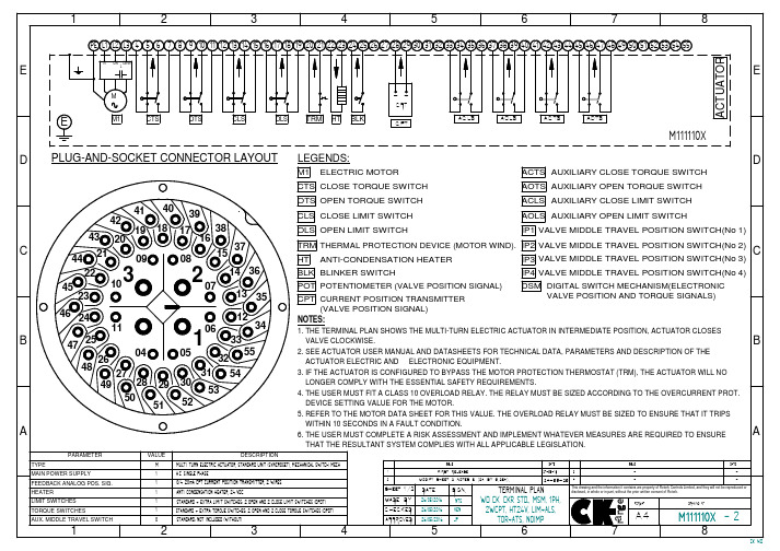
OPEN by limit switching / CLOSE by torque switching • CTS and OTS act as overload protection for the whole stroke, they interrupt the
control circuit when reaching the actuator set tripping torque. • OLS interrupts the control circuit when reaching the valve open limit set position. • CTS interrupts the control circuit when closing (seating) the valve. Set the close
MADE BY 26/05/2016 NTS CHECKED 26/05/2016 VEN APPROVED 26/05/2016 JP
WD CK-CKR STD., MSM, 1PH, 2WCPT, HT24V, LIM+ALS,
TOR+ATS, NOIMP
range
FLTI-TURN ELECTRIC ACTUATOR, STANDARD UNIT (SYNCROSET), MECHANICAL SWITCH MECH. A.C. SINGLE PHASE
0/4-20mA CPT CURRENT POSITION TRANSMITTER, 2 WIRES
ANTI-CONDENSATION HEATER, 24 VDC
A NOTES: 1. THE TERMINAL PLAN SHOWS THE ELECTRIC ACTUATOR IN INTERMEDIATE POSITION, ACTUATOR CLOSES VALVE CLOCKWISE 2. SEE ACTUATOR USER MANUAL FOR TECHNICAL DATA, PARAMETERS AND DESCRIPTION OF THE ACTUATOR ELECTRIC AND ELECTRONIC EQUIPMENT.
同步器设计手册

同步器设计手册前言汽车变速器中采用同步器,可以保证换档操作迅速、轻便无冲击,延长齿轮和传动系统的使用寿命,提高汽车在换档和加速起步时的动力性和经济性,改善驾驶舒适性的有效措施。
同步器技术目前被广泛应用于各种车型上。
同步器的应用是机械变速器发展过程中一次质的飞跃,在我国汽车行业标准QC/T29063中明确规定轻型汽车变速器前进档必需装有同步器结构,中型汽车除一档、倒档外,其余各档也必需装有同步器结构。
随着同步器技术不断发展,对于提高变速器传动性能,具有十分重要的经济技术意义。
本手册是在综合同步器理论和实践研究的基础上编写而成。
本书结构新颖,文字简洁,图文并茂,通俗易懂。
内容包括:同步器结构形式,工作原理,设计参数,结构参数,以及影响同步器性能的因素。
本手册可供从事汽车变速器的设计、生产、维修人员参考。
本手册经等人员审阅并提出修改意见,在此表示感谢。
由于作者水平有限,难免有不足之处,请广大员工提出宝贵意见。
作者2007/11/16目录绪论第一章同步器的结构形式及其特点第一节锁销式同步器第二节锁环式同步器第三节锁环式多锥同步器第二章同步器工作原理第三章同步器设计参数及其计算第一节转动惯量及其转换第二节同步力矩 Tc及同步时间第三节拨环力矩T B第四节计算实例第四章结构参数设计第一节结构参数设计第二节结构参数设计对换档性能的影响第三节同步器摩擦材料第五章影响同步器性能的因素第一节润滑油对同步器性能的影响第二节其他对同步器性能的影响第六章同步器试验绪 论汽车变速器是汽车传动系中的一个重要部件,它的功能是在不同的使用条件下,改变由发动机传到驱动轮上的转矩和转速,使得汽车得到不同的牵引力和车速,以适应不同的使用条件。
同时也可以使发动机在最有利的工况范围内工作。
为保证变速器具有良好的工作性能,对变速器提出以下基本要求:1. 应有合适的变速档位数和传动比,保证汽车具有良好的动力性和经济性指标。
2. 较高的传动效率。
同步器

谢谢观看
由此可见,用常压式同步器换档与用接合套换档比较,在工作过程上的区别,主要在于前者的摩擦作用能使需 接合的两花键齿圈迅速地达到并保持同步。
惯性式同步器与常压式同步器一样,都是依靠摩擦作用实现同步。但它可以从结构上保证接合套与待接合的 花键齿圈在达到同步之前不可能接触,以避免齿间冲击和发生噪声。
惯性式同步器广泛应用于轿车和轻、中型货车的变速器中。常用的结构形式有锁环式惯性同步器和锁销式惯 性同步器两种。
只要接合套与待啮合齿轮之间存在转速差,弹簧片的支承力就阻止同步环直径缩小,因而也就阻止了接合套 移动。在二者的转速差为零(同步)时,弹簧片卸除载荷,即以右弹簧片的上端为支点,弹簧片伸张,其下端顶 住支承块凸起右侧,推动接合齿圈连同低档齿轮一道顺时针方向转动一个角度,使弹簧片松弛,于是阻止同步环 直径缩小的支承力消失。此时,在不大的换档力作用下,接合套便可压缩同步环,与右侧的接合齿圈接合,而同 步环处于接合套的屋顶状凹槽里,被可靠地定位。因此,在挂档位置,毋需采用一般变速器所必须设置的自锁装 置。
常压式同步器在齿轮2与4接合齿圈相对的一侧均有一个外锥面。相应地在花键毂两侧加工出内锥面。在花键 毂的径向孔内,装有定位销6,它借弹簧的压力嵌入在接合套3内切出的环形凹槽中。图1上部的三个图为在挂直 接档的过程中同步器的工作示意图。图1a表示接合套在空档位置。挂直接档时,向左拨动接合套,则通过定位销 带动花键毂1一同左移。当花键毂的内锥面与齿轮2的外锥面接触时,花键毂即不能再继续左移。由于接合套与花 键毂之间有弹簧顶住的定位销6,若驾驶员作用在接合套上的力不大,则定位销便阻止接合套在花键毂停止不动的 情况下继续向左移动。此时位置如图1b所示。两锥匦在驾驶员通过操纵机构加于接合套和花键毂上的力的作用下 互相压紧。齿轮2与花键毂存在转速差,因而两锥面一经接触,便产生摩擦作用。这种摩擦作用促使第一轴齿轮的 转速迅速降低到与花键毂的转速(亦即接合套的转速)相等,因而二者花键齿的圆周速度相等(同步)。此时驾 驶员继续增大加于接合套上的推力,使接合套克服弹簧力压下定位销6而相对花键毂继续左移,其内花键齿圈便与 齿轮 &的接合齿圈接合,即挂入直接档,如图1c所示。
同步器图文详解
三轴五当变速器传动简图1-输入轴 2-轴承 3-接合齿圈 4-同步环 5-输出轴 6-中间轴 7-接合套 8-中间轴常啮合齿轮此变速器有五个前进档和一个倒档,由壳体、第一轴(输入轴)、中间轴、第二轴(输出轴)、倒档轴、各轴上齿轮、操纵机构等几部分组成。
两轴五当变速器传动简图1-输入轴 2-接合套 3-里程表齿轮 4-同步环 5-半轴 6-主减速器被动齿轮 7-差速器壳 8-半轴齿轮 9-行星齿轮 10、11-输出轴 12-主减速器主动齿轮 13-花键毂与传统的三轴变速器相比,由于省去了中间轴,所以一般档位传动效率要高一些;但是任何一档的传动效率又都不如三轴变速器直接档的传动效率高。
同步器有常压式,惯性式和自行增力式等种类。
这里仅介绍目前广泛采用的惯性式同步器。
惯性式同步器是依靠摩擦作用实现同步的,在其上面设有专设机构保证接合套与待接合的花键齿圈在达到同步之前不可能接触,从而避免了齿间冲击。
惯性同步器按结构又分为锁环式和锁销式两种。
其工作原理可以北京BJ212型汽车三档变速器中的二、三档同步器为例说明。
花键毂7与第二轴用花键连接,并用垫片和卡环作轴向定位。
在花键毂两端与齿轮1和4之间,各有一个青铜制成的锁环(也称同步环)9和5。
锁环上有短花键齿圈,花键齿的断面轮廓尺寸与齿轮 1,4及花键毂 7上的外花键齿均相同。
在两个锁环上,花键齿对着接合套8的一端都有倒角(称锁止角),且与接合套齿端的倒角相同。
锁环具有与齿轮1和4上的摩擦面锥度相同的内锥面,内锥面上制出细牙的螺旋槽,以便两锥面接触后破坏油膜,增加锥面间的摩擦。
三个滑块2分别嵌合在花键毂的三个轴向槽11内,并可沿槽轴向滑动。
在两个弹簧圈6的作用下,滑块压向接合套,使滑块中部的凸起部分正好嵌在接合套中部的凹槽10中,起到空档定位作用。
滑块2的两端伸入锁环9和5的三个缺口12中。
只有当滑块位于缺口12的中央时,接合套与锁环的齿方可能接合。
前置发动机后轮驱动汽车变速器的外操纵机构1-变速器壳体 2-变速连动杆 3-变速杆。
Woodword同步器 中文说明书
WoodwordSPM-A同步器安装操作和标准手册内容第一章概述……………………………………………………………..….警告注意事项…………………………………………………………....符合EMC标准………………………………………………...………介绍…………………………………………………………………….描述……………………………………………………………………..操作原理……………………………………………………………...….同步器输入端………………………………………………………….操作模式……………………………………………………………...发电机同步……………………………………………………………电压匹配……………………………………………………………... 第二章放电须知……………………………………………………………第三章安装验货………………………………………………………………………..位置……………………………………………………………………….安装……………………………………………………………………….电气接线…………………………………………………………………..至发电机的接线…………………………………………………………..至负荷分配器和速度控制器的连线……………………………………..最优速度输出…………………………………………………………母线-母线并机………………………………………………………...使发电机投入母线……………………………………………………电压调节继电器输出接线……………………………………………并机断路器和闸接线…………………………………………………第四章标准与核查概述…………………………………………………………………..预检查…………………………………………………………………滞后时间调节…………………………………………………………测试和调整……………………………………………………………试验台调节………………………………………………………动态检查………………………………………………………………稳定性和增益调节…………………………………………….频率调节……………………………………………………….偏移调节………………………………………………………..相位偏移调节………………………………………………….电压偏移调节…………………………………………………. 第五章服务产品服务选项………. …………………………..…………………返回设备修理…….. ……………….………………………………控制器包装…….. …………………….……………………………授权系列号…………………………………………………………替代部分…………………………………………………………..联系Woodward……………………………………………….….产品售后服务…………………………………………………….Woodward规范…………………………………………………..安装接线图……………………………………. 1-1 控制接线概述……………………………………………………. 1-2 系统方框图………………………………………………………1-3 功能方框图………………………………………………………1-4 出厂接线图………………………………………………………3-1 典型SPM-A同步接线…………………………………………. 3-2母线-母线并接………………………………………………. 3-3滞后时间设置………………………………………………..第一章概述常规注意事项●根据加拿大CSA和美国的UL标准,SPM-A一般安装在无危险的位置。
同步器设计
第五节同步器设计同步器有常压式、惯性式和惯性增力式三种。
常压式同步器结构虽然简单,但有不能保证啮合件在同步状态下(即角速度相等)换挡的缺点,现已不用。
得到广泛应用的是惯性式同步器。
一、惯性式同步器惯性式同步器能做到换挡时两换挡元件之间的角速度达到完全相等之前,不允许换挡,因而能完善地完成同步器的功能和实现对同步器的基本要求。
按结构分,惯性式同步器有锁销式、滑块式、锁环式、多片式和多锥式几种。
虽然它们的结构不同,但都有摩擦元件、锁止元件和弹性元件。
图3—17a所示锁销式同步器的摩擦件是同步环2和齿轮3上的凸肩部分,分别在它们的内圈和外圈设计有相互接触的锥形摩擦面。
锁止元件位于滑动齿套1的圆盘部分孔中做出的锥形肩角和装在上述孔中、在中部位置处有相同角度的斜面锁销4。
锁销与同步环2刚性连接。
弹性元件是位于滑动齿套1圆盘部分径向孔中的弹簧7。
在空挡位置,钢球5在弹簧压力作用下处在销6的凹槽中,使之保持滑动齿套与同步环之间没有相对移动。
滑动齿套与同步环之间为弹性连接。
图3—17b所示锁环式同步器摩擦元件,是通过滑动齿套8及锁环9上的锥面来实现的。
作为锁止元件是锁环9的内齿和做在齿轮10上的接合齿端部。
齿轮10和锁环9之间是弹性连接。
图3—17 惯性式同步器结构方菜a)锁销式 b)锁环式1、8--滑动齿套 2--同步环 3、10--齿轮 4--锁销5--钢球 6--销 7--弹簧 9--锁环在惯性式同步器中,弹性元件的重要性仅次于摩擦元件和锁止元件,它用来使有关部分保持在中立位置的同时,又不妨碍锁止、解除锁止和完成换挡的进行。
锁销式同步器的优点是零件数量少,摩擦锥面平均半径较大,使转矩容量增加。
这种同步器轴向尺寸长是它的缺点。
锁销式同步器多用于中、重型货车的变速器中。
滑块式同步器本质上是锁环式同步器,它工作可靠、零件耐用;但因结构布置上的限制,转矩容量不大,而且由于锁止面在同步锥环的接合齿上,会因齿端磨损而失效,因而主要用于轿车和轻型货车变速器中。
三通道10输入18输出系统同步器说明书
ZL30671, ZL30672, ZL306731-, 2-, 3-Channel, 10-Input, 18-OutputSystem SynchronizersProduct BriefNovember 2019 Features•One, Two or Three DPLL Channels•Timing compliance with ITU-T G.8262, G.813,G.812, G.8273.2; Telcordia GR-1244, GR-253•Programmable bandwidth, 0.1mHz to 470Hz•Freerun or holdover on loss of all inputs•Hitless reference switching•High-resolution holdover averaging•Per-DPLL phase adjustment, 1ps resolution•Programmable tracking range, phase-slope limiting, frequency-change limiting and otheradvanced features•Input Clocks•Accepts up to 10 differential or CMOS inputs•Any input frequency from 0.5Hz to 900MHz•Per-input activity and frequency monitoring•Automatic or manual reference switching•Revertive or nonrevertive switching•Any input can be a 1PPS SYNC input for REF+SYNC frequency/phase/time locking •Input-input phase measurement, 1ps resolution •Input-DPLL phase measurement, 1ps resolution •Per-input phase adjustment, 1ps resolution•Output Clock Frequency Generation•Any output frequency from <0.5Hz to 1045MHz (180MHz max for Synth0)•High-resolution fractional frequency conversion with 0ppm error•Synthesizers 1 & 2 have integer and fractional dividers to make a total of 5 frequency families •Output jitter from Synth 1 & 2 is <0.3ps RMS•Output jitter from fractional dividers is typically < 1ps RMS, many frequencies <0.5ps RMS •Each HPOUTP/N pair can be LVDS, LVPECL, HCSL, 2xCMOS, HSTL or programmable diff.•In 2xCMOS mode, the P and N pins can be different frequencies (e.g. 125MHz and 25MHz) •Four output banks each with VDDO pin; CMOS output voltages from 1.5V to 3.3V•Per-synthesizer phase adjust, 1ps resolution•Per-output programmable duty cycle•Precise output alignment circuitry and per-output phase adjustment•Per-output enable/disable and glitchlessstart/stop (stop high or low)•Local Oscillator•Operates from a single TCXO or OCXO: 23.75-25MHz, 47.5-50MHz, 114.285-125MHz •Very-low-jitter applications can connect a TCXO or OCXO as the stability reference and a low-jitter XO as the jitter reference•General Features•Automatic self-configuration at power-up from internal Flash memory•Input-to-output alignment <200ps (ext feedback) •Fast REF+SYNC locking for frequency and 1PPS phase alignment with lower-cost oscillator •Internal compensation (1ppt) for local oscillator frequency error in DPLLs and input monitors •Numerically controlled oscillator behavior in each DPLL and each fractional output divider•Easy-to-configure design requires no external VCXO or loop filter components•7 GPIO pins with many possible behaviors•SPI or I2C processor Interface• 1.8V and 3.3V core VDD voltages•Power: 1.3W for 2 inputs, 1 synth, 6 LVDS out•Easy-to-use evaluation/programming software Applications•Central system timing ICs for SyncE,SyncE+1588, SONET/SDH, OTN, wirelessbase station and other carrier-grade systems •G.8262/813 EEC/SEC, Telcordia Stratum 2-4Ordering InformationZL30671LFG7 1-Channel 80-lead LGA TraysZL30672LFG7 2-Channel 80-lead LGA TraysZL30673LFG7 3-Channel 80-lead LGA TraysNiAu (Pb-free)Package size: 11 x 11 mm-40︒C to +85︒C1. Block DiagramFigure 1 - Functional Block Diagram2. Application ExampleFigure 2 - Synchronous Ethernet and IEEE 1588 Central Timing ApplicationFracDiv IntDiv FracDivIntDivHP Synthesizer 2low-jitterHPOUT6P HPOUT6N HPOUT7P HPOUT7NDIVREF0P DPLL0R S T _BC S _B _A S E L 0S C K _S C LS O _A S E L 1S I _S D AG P I O [8:0]Microprocessor Port SPI or I2C I/F & GPIO Pins One Diff / Two Single-Ended REF0N REF1P One Diff / Two Single-Ended REF1N REF2P One Diff / Two Single-EndedREF2NREF3P One Diff / Two Single-Ended REF3N REF4P One Diff / Two Single-EndedREF4NReference Monitors & State MachinesDPLL1DPLL2HP Synthesizer 1low-jitterGP Synthesizer 0general purpos eGPOUT0GPOUT1DIV DIVXO Optional x2O S C IO S C OMaster Clock M C L K I N _PDIVHPOUT4P HPOUT4N HPOUT5P HPOUT5N DIV DIVHPOUT0P HPOUT0N HPOUT1P HPOUT1N DIVDIV HPOUT2P HPOUT2N HPOUT3P HPOUT3NDIVDIVM C L K I N _NS R S T _BGPS (1PPS)BITS/SSU Line Extracted Clocks[7:0]TCXODPLL0T4 pathSynth01.544 or2.048MHz CMOS to BITS/SSU1 PPSDPLL1SyncESynth12x 156.25MHz 2x 125MHz155.52MHz, 161.1328125MHz or other frequencyDPLL21588Control info from IEEE 1588 algorithmSynth225MHz 1 PPS or clock w/ embedded PPS 1588 signals to system componentsSyncE signals to system componentsto BITS/SSU systemDPLL1 only present on ZL30672 and ZL30673 DPLL2 only present on ZL306733. Detailed Features3.1 Input Block Features•Ten input reference pins; each can accept a CMOS signal or the POS side of a differential pair; or two can be paired to accept both sides of a differential pair•Any input can be a SYNC signal for REF+SYNC frequency/phase/time locking•Input clocks can be any frequency from 0.5Hz up to 900MHz (180MHz max for CMOS inputs)•Supported telecom frequencies include PDH, SDH, Synchronous Ethernet, OTN, wireless•Inputs constantly monitored by programmable frequency and single-cycle monitors•Single-cycle monitor can quickly disqualify a reference when measured period is incorrect•Frequency measurement (ppb or Hz) and monitoring (coarse, fine, and frequency-step monitors)•Optional input clock invalidation on GPIO assertion to react to LOS signals from PHYs•Input-to-input phase measurement, 1ps resolution•Input-to-DPLL phase measurement, 1ps resolution•Per-input phase adjustment, 1ps resolution3.2 DPLL Features•One, two or three full-featured DPLLs•Very high-resolution DPLL architecture•State machine automatically transitions among freerun, tracking and holdover states•Revertive or nonrevertive reference selection algorithm•Programmable bandwidth from 0.1mHz to 470Hz•Less than 0.1dB gain peaking•Fast frequency/phase/time lock capability for 1PPS or clock+1PPS input references•Programmable phase-slope limiting (PSL)•Programmable frequency rate-of-change limiting (FCL)•Programmable tracking range (i.e. hold-in range)•Truly hitless reference switching•Per-DPLL phase adjustment, 1ps resolution•High-resolution frequency and phase measurement•Fast detection of input clock failure and transition to holdover mode•High-resolution holdover frequency averaging•Time-of-Day registers: 48-bit seconds, 32-bit nanoseconds, writeable on input PPS edge3.3 Synthesizer Features•Any-to-any frequency conversion with 0ppm error•Two low-jitter synthesizers (Synth1, Synth2) with very high-resolution fractional scaling (i.e. non-integer multiplication)•Two output dividers per low-jitter synthesizer: one integer (4 to 15 plus half divides 4.5 to 7.5) and one 40-bit fractional•One general-purpose synthesizer (Synth0)• A total of five output frequency families•Easy-to-configure, completely encapsulated design requires no external VCXO or loop filter components3.4 Low-Jitter Output Clock Features•Up to 16 single-ended outputs (up to 8 differential outputs) from Synth1 and Synth2•Each output can be one differential output or two CMOS outputs•Output clocks can be any frequency from 0.5Hz to 1045MHz (250MHz max for CMOS and HSTL)•Output jitter from Synth1 and Synth2 integer dividers is <0.3ps RMS•Output jitter from fractional dividers is <1ps RMS, many frequencies <0.5ps RMS•In CMOS mode, the HPOUTxN frequency can be an integer divisor of the HPOUTxP frequency (Example 1: HPOUT3P 125MHz, HPOUT3N 25MHz. Example 2: HPOUT2P 25MHz, HPOUT2N 1Hz) •Outputs directly interface (DC coupled) with LVDS, LVPECL, HSTL, HCSL and CMOS components•Supported telecom frequencies include PDH, SDH, Synchronous Ethernet, OTN•Can produce clock frequencies for microprocessors, ASICs, FPGAs and other components•Can produce PCIe clocks•Sophisticated output-to-output phase alignment•Per-synthesizer phase adjustment, 1ps resolution•Per-output phase adjustment•Per-output duty cycle / pulse width configuration•Per-output enable/disable•Per-output glitchless start/stop (stop high or low)3.5 General-Purpose Output Clock Features•Two CMOS outputs from Synth0•Any frequency from 0.5Hz to 180MHz•Output jitter is typically 20-30ps•Useful for applications where the component or system receiving the signal has low bandwidth such asa central timing IC•Can output a clock signal with embedded PPS (ePPS) (duty cycle distortion indicates PPS location) 3.6 Local Oscillator•Operates from a single TCXO or OCXO (jitter reference for the device). Acceptable frequencies:23.75MHz to 25MHz, 47.5MHz to 50MHz, 114.285MHz to 125MHz. Best jitter: ≥48MHz.•Very-low-jitter applications can connect a TCXO or OCXO (any frequency, any output jitter) as the stability reference and a low-cost low-jitter XO as the jitter reference•This ability to have separate jitter and stability references greatly reduces the cost of the TCXO or OCXO (no jitter requirement, no high-frequency-requirement) and allows reuse of already-qualifiedTCXO and OCXO components•Supports redundant TCXOs connected to two REF pins3.7 General Features•Automatic self-configuration at power-up from internal Flash memory•Input-to-output alignment <200ps with external feedback•Fast REF+SYNC locking for frequency and 1PPS phase alignment with lower-cost oscillator•Generates output SYNC signals: 1PPS (IEEE 1588), 2kHz or 8kHz (SONET/SDH) or other frequency •JESD204B clocking: device clock and SYSREF signal generation with skew adjustment•Internal compensation for local oscillator frequency error in DPLLs and input monitors, 1ppt resolution •Numerically controlled oscillator (NCO) behavior allows system software to steer DPLL frequency or fractional output divider frequency with resolution better than 0.005ppt•Spread-spectrum modulation available in each fractional output divider (PCIe compliant)•Seven general-purpose I/O pins each with many possible status and control options•SPI or I2C serial microprocessor interface3.8 Evaluation Software•Simple, intuitive Windows-based graphical user interface•Supports all device features and register fields•Makes lab evaluation of the device quick and easy•Generates configuration scripts to be stored in internal Flash memory•Generates full or partial configuration scripts to be run on a system processor•Works with or without an evaluation board4. Package Outline DrawingSYM COMMON DIMENSIONSMIN NOR. MAX.TOTAL THICKNESS A --- --- 0.9SUBSTRATE THICKNESS A1 0.21 REFMOLD THICKNESS A2 0.54 REFBODY SIZE D 11 BSCE 11 BSCLEAD WIDTH W 0.2 0.25 0.3 LEAD LENGTH L 0.35 0.4 0.45 EP WIDTH W1 1.6 1.65 1.7 EP LENGTH L1 1.6 1.65 1.7 LEAD PITCH e 0.5 BSC EP PITCH e1 1.8 BSC LEAD COUNT n 80EP COUNT n1 16EDGE LEAD CENTER TO CENTER D1 9.5 BSC E1 9.5 BSCBODY CENTER TO CENTER LEAD SD 0.25 BSC SE 0.25 BSCBODY CENTER TO CENTER EP SD1 0.9 BSC SE1 0.9 BSCPRE-SOLDER --- --- --- PACKAGE EDGE TOLERANCE aaa 0.1MOLD FLATNESS bbb 0.1 COPLANARITY ddd 0.08Microsemi Corporate Headquarters One EnterpriseAliso Viejo, CA 92656 USAWithin the USA: +1 (800) 713-4113 Outside the USA: +1 (949) 380-6100 Sales: +1 (949) 380-6136Fax: +1 (949) 215-4996E-mail: ***************************©2019 Microsemi Corporation. All rights reserved. Microsemi and the Microsemi logo are trademarks of Microsemi Corporation. All other trademarks and service marks are the property of their respective owners. Microsemi Corporation (Nasdaq: MSCC) offers a comprehensive portfolio of semiconductor and system solutions for communications, defense & security, aerospace and industrial markets. Products include high-performance and radiation-hardened analog mixed-signal integrated circuits, FPGAs, SoCs and ASICs; power management products; timing and synchronization devices and precise time solutions, setting the world’s standard for time; voice processing devices; RF solutions; discrete components; security technologies and scalable anti-tamper products; Power-over-Ethernet ICs and midspans; as well as custom design capabilities and services. Microsemi is headquartered in Aliso Viejo, Calif., and has approximately 3,400 employees globally. Learn more at .Microsemi makes no warranty, representation, or guarantee regarding the information contained herein or the suitability of its products and services for any particular purpose, nor does Microsemi assume any liability whatsoever arising out of the application or use of any product or circuit. The products sold hereunder and any other products sold by Microsemi have been subject to limited testing and should not be used in conjunction with mission-critical equipment or applications. Any performance specifications are believed to be reliable but are not verified, and Buyer must conduct and complete all performance and other testing of the products, alone and together with, or installed in, any end-products. Buyer shall not rely on any data and performance specifications or parameters provided by Microsemi. It is the Buyer’s responsibility to independently determine suitability of any products and to test and verify the same. The information provided by Microsemi hereunder is provided “as is, where is” and with all faults, and the entire risk associated with such information is entirely with the Buyer. Microsemi does not grant, explicitly or implicitly, to any party any patent rights, licenses, or any other IP rights, whether with regard to such information itself or anything described by such information. Information provided in this document is proprietary to Microsemi, and Microsemi reserves the right to make any changes to the information in this document or to any products and services at any time without notice.。
- 1、下载文档前请自行甄别文档内容的完整性,平台不提供额外的编辑、内容补充、找答案等附加服务。
- 2、"仅部分预览"的文档,不可在线预览部分如存在完整性等问题,可反馈申请退款(可完整预览的文档不适用该条件!)。
- 3、如文档侵犯您的权益,请联系客服反馈,我们会尽快为您处理(人工客服工作时间:9:00-18:30)。
前言
汽车变速器中采用同步器,可以保证换档操作迅速、轻便无冲击,延长齿轮和传动系统的使用寿命,提高汽车在换档和加速起步时的动力性和经济性,改善驾驶舒适性的有效措施。同步器技术目前被广泛应用于各种车型上。同步器的应用是机械变速器发展过程中一次质的飞跃,在我国汽车行业标准QC/T29063中明确规定轻型汽车变速器前进档必需装有同步器结构,中型汽车除一档、倒档外,其余各档也必需装有同步器结构。随着同步器技术不断发展,对于提高变速器传动性能,具有十分重要的经济技术意义。
对于二档换一档的退档过程中,同理是齿轮P1和S1的减速度要比齿轮P2和S2要大。所以高档换低档是极其复杂的。在分开二档齿轮之前,齿轮S1的圆周线速度VS1比齿轮S2、P2、P1要大,如图3所示,齿轮P2和P1在t′x 时趋于零,齿轮S2和S1在tx 时趋于零,他们之间相距很大。根本不能相交,齿轮P1和S1圆周线速度永远没有相等的时间。所以,要想在瞬间内使这两个齿轮直接相啮合是不可能的。必须采取一种辅助方法使齿轮P1和S1圆周线速度接近。这就是通常的做法“两脚离合器”:
第一步踩下离合器踏板;
第二步将排档杆移至空档位置;
第三步再松开离合器踏板,稍加油门从a→b,使齿轮p1速度增高并超过齿轮S1的速度线。
第四步再踩下离合器踏板b→C,使齿轮p1速度迅速下降,在C点迅速换档。
这样就找到了时间t2 点,使齿轮P1和S1圆周线速相等。在这个过程中,驾驶员不但要有高超的实践经验和操作技能,而且劳动强度也很大。
汽车机械式变速器安装了同步器之后,就不需要“两脚离合器”的操作。减轻了驾驶员的劳动强度,减少换档时齿轮间的撞击,能准确无误地换档,增加了舒适性。
同步器发展仅有数十年的历史。自1912年奥地利的Humohries提出了采用摩擦式同步器之后,直到1926年才装到美国凯迪莱克汽车上。从此之后使用范围不断扩大,到目前为止凡是手动机械式汽车变速器都使用了同步器。
本手册是在综合同步器理论和实践研究的基础上编写而成。本书结构新颖,文字简洁,图文并茂,通俗易懂。内容包括:同步器结构形式,工作原理,设计参数,结构参数,以及影响同步器性能的因素。本手册可供从事汽车变速器的设计、生产、维修人员参考。
本手册经等人员审阅并提出修改意见,在此表示感谢。由于作者水平有限,难免有不足之处,请广大员工提出宝贵意见。
早期开发的同步器为常压式同步器,有锥形和片式两种。由于它不能保证被啮合齿轮在同步状态(即角速度相等)下实现换档,不能从根本上解决换档时啮合冲击问题,所以这种同步器目前已被淘汰。
目前汽车上广泛使用的惯性式同步器,主要有:锁销式同步器;锁环式同步器;锁环式多锥面同步器。除此以外还有增压式同步器。由于这种同步器对材料、热处理及制造精度均要求较高,目前国内采用较少。近几年来国外还开发了一种杠杆式同步器,主要用于倒档。这种同步器还处于试验状态中。下面分锁销式同步器、锁环式同步有良好的工作性能,对变速器提出以下基本要求:
1.应有合适的变速档位数和传动比,保证汽车具有良好的动力性和经济性指标。
2.较高的传动效率。
3.应有空档和倒档。
4.换档操纵迅速轻便、工作可靠,噪声小。
在手动机械式变速器中(Manual Transmission简称MT),同步器是改善换档性能的主要零部件。对减轻驾驶员的劳动强度,使操纵轻便,提高齿轮及传动系统的使用寿命,提高汽车行驶安全性和乘坐的舒适性,改善汽车起步时的加速性和经济性起着重要作用。
作者
2007/11/16
绪论
第一章同步器的结构形式及其特点
第一节锁销式同步器
第二节锁环式同步器
第三节锁环式多锥同步器
第二章同步器工作原理
第三章同步器设计参数及其计算
第一节转动惯量及其转换
第二节同步力矩Tc及同步时间
第三节拨环力矩TB
第四节计算实例
第四章结构参数设计
第一节结构参数设计
第二节结构参数设计对换档性能的影响
现以一个五档变速器为例,说明同步器在换档中的作用。
假如汽车正在二档位置上行驶,则变速器通过发动机传来的动力,经过第一轴上的齿轮A和中间轴常啮合齿轮B、齿轮P2传递给第二轴上的齿轮S2,使动力输出。这时齿轮P2和齿轮S2的圆周线速度相等,VS2=VP2。当汽车在良好的路面行驶,驾驶员此时要改善汽车行驶的经济性,要从二档换到三档上行驶,这时驾驶员就要把齿轮S2和P2分开,而把齿轮S3和P3接合上。此时中间轴上的齿轮P3的直径要比P2大。由于中间轴传动角速度ω不变,则Vp3>VP2。同理,由于第二轴上的齿轮S3的直径小于S2的直径,VS3<VS2。如果在时间t内踩离合器,由于第二轴与驱动桥、后轮、整车相连,转动惯量很大,齿轮的速度不可能很快降下来。这样,在时间t内,齿轮S2和S3的圆周线速度不相等,见图2所示。要经过相当长的时间tx,等后轮轴停止后,齿轮S2和S3的圆周线速度相等,同时为零。
同步器自问世以来,结构在不断变化,工作性能也在日趋完善。近些年来国外在同步器研究、设计、制造方面发展很快。我们在自主研发、制造与国外相比还存在很大差距,同步器的性能和可靠性还不能满足使用要求。因此我们要加强同步器方面的研究,缩小差距,力争赶超和超过国外先进水平。
第一章同步器的结构型式及其特点
汽车变速器中使用同步器,可以保证换档时齿轮不受冲击,延长齿轮的使用寿命,使汽车在起步、换档时的加速度和经济性得到改善。换档时加在齿套上的轴向力经柱销(或滑块)推动同步环使锥面相接触产生摩擦力矩,借此改变被啮合齿轮的转速以达到同步。
对于中间轴,是齿轮A、B随第一轴即离合器而转动。由于这一段的转动惯量小,离合器分离后,会在很短时间t′x 内停止转动,Vp3和VP2很快随第一轴的停止而趋于零。
当中间轴与第二轴以不同的速度降低的过程中,齿轮P3和S3圆周线速度相等,驾驶员就要巧妙地抓住这段时间,把齿轮P3和齿轮S3接合上。所以在低档换高档的过程中,全靠驾驶员的熟练操作和丰富经验,同时注意力也要特别集中。
第三节同步器摩擦材料
第五章影响同步器性能的因素
第一节润滑油对同步器性能的影响
第二节其他对同步器性能的影响
第六章同步器试验
绪论
汽车变速器是汽车传动系中的一个重要部件,它的功能是在不同的使用条件下,改变由发动机传到驱动轮上的转矩和转速,使得汽车得到不同的牵引力和车速,以适应不同的使用条件。同时也可以使发动机在最有利的工况范围内工作。