Invensense三轴陀螺仪 MPU-3050MPU-3000
2024年汽车IMU传感器市场发展现状

汽车IMU传感器市场发展现状概述汽车IMU(惯性测量单元)传感器是一种用于测量和监测汽车运动和姿态的设备。
它根据汽车的加速度和角速度等参数来提供精确的定位和导航信息。
随着自动驾驶和智能交通系统的发展,汽车IMU传感器市场迅速崛起并展现出巨大的潜力。
本文将对汽车IMU传感器市场的发展现状进行分析和总结。
发展趋势自动驾驶技术的兴起随着自动驾驶技术的不断进步和成熟,对高精度定位和导航的需求越来越大,而汽车IMU传感器作为一种重要的组成部分,正成为实现自动驾驶的关键技术之一。
因此,汽车IMU传感器市场在自动驾驶技术的推动下呈现出迅猛发展的趋势。
智能交通系统的发展除了自动驾驶技术,智能交通系统的发展也对汽车IMU传感器市场的增长起到了推动作用。
智能交通系统涉及到交通流量监测、车辆跟踪、道路状态检测等方面,而这些功能都离不开精确的位置和姿态信息,而汽车IMU传感器正是提供这些信息的重要设备。
市场规模根据市场研究公司的数据,汽车IMU传感器市场的规模呈现出快速增长的趋势。
2019年,全球汽车IMU传感器市场的规模达到X亿美元,预计到2025年将达到X 亿美元。
亚洲地区是全球汽车IMU传感器市场的主要消费地区,北美地区也表现出较高的市场增长率。
主要厂商和产品目前,全球汽车IMU传感器市场上存在着众多的厂商和产品,其中一些领先的厂商和产品包括:1.Bosch Sensortec:Bosch Sensortec是汽车IMU传感器市场的领先供应商之一,其产品包括BMA456和BMI270等系列产品。
2.STMicroelectronics:STMicroelectronics是另一家在汽车IMU传感器市场中占据重要地位的厂商,其产品包括LSM6DSL和LSM330等系列产品。
3.InvenSense:InvenSense是一家知名的汽车IMU传感器供应商,其产品包括MPU-6050和MPU-9250等系列产品。
技术进展汽车IMU传感器市场的发展受益于技术的进步和创新。
InvenSense技术

InvenSense技术概述本公司拥有五种主要的专有技术优势:专利的Nasiri-Fabrication制程、先进的MEMS运动感测组件设计、为传感器讯号处理(sensor signal processing)的混合讯号电路系统(mixed-signal circuitry)、运动感测融合演算(MotionFusion)与校正韧件(calibration firmware)、可为所有消费性电子产品操作系统的应用开发业者提供含有驱动程序与APIs的运动感测应用(MotionApp)软件。
本公司专利的Nasiri-Fabrication制程,可在晶圆层级结合MEMS机械结构与标准CMOS(互补金属氧化物半导体:complementary metal oxide semiconductor),使本公司产品在性能、可靠度、整合度、与价格上,具有明显的优势,并让InvenSenseihs 成为业界第一个采取商业MEMS 无晶圆厂经营模式、拥有高产能的公司。
本公司混合讯号电路系统支援感测讯号处理,驱动运动感测处理(MotionProcessing)平台的关键-运动感测融合演算技术。
本公司的技术,能够为如智能型手机、平板电脑、游戏摇杆、智能型电视与配戴式传感器等所有消费性电子应用产品,提供运动感测人机界面(Motion Interface)解决方案。
而且,整合等级的提升,让本公司能提供从一轴模拟陀螺仪到完整整合之智能型六轴与九轴运动感测追踪(MotionTracking)组件等的产品。
制程平台比较│点选放大本公司专利的Nasiri-Fabrication制程平台使本公司得以提供高整合与低成本的产品本公司运动感测追踪(MotionTracking)组件的基础关键技术为专利的Nasiri-Fabrication制程,将MEMS和CMOS直接整合(即CMOS-MEMS) 于小尺寸、低成本的标准包装内。
MEMS晶圆与工业标准CMOS晶圆的直接整合,减少了MEMS制程步骤、在晶圆阶级进行测试、使用芯片层级包装,不但降低了后段包装成本及测试成本,也改善了整体产能与质量。
微机械MEMS陀螺仪原理和几大公司的基本工艺流程
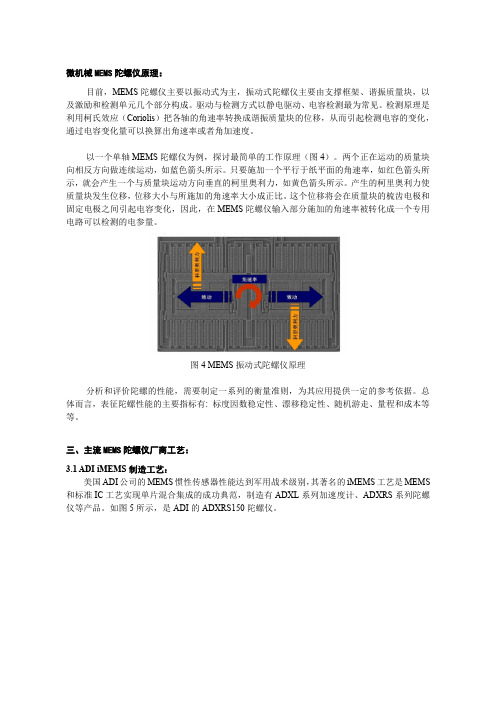
微机械MEMS陀螺仪原理:目前,MEMS陀螺仪主要以振动式为主,振动式陀螺仪主要由支撑框架、谐振质量块,以及激励和检测单元几个部分构成。
驱动与检测方式以静电驱动、电容检测最为常见。
检测原理是利用柯氏效应(Coriolis)把各轴的角速率转换成谐振质量块的位移,从而引起检测电容的变化,通过电容变化量可以换算出角速率或者角加速度。
以一个单轴MEMS陀螺仪为例,探讨最简单的工作原理(图4)。
两个正在运动的质量块向相反方向做连续运动,如蓝色箭头所示。
只要施加一个平行于纸平面的角速率,如红色箭头所示,就会产生一个与质量块运动方向垂直的柯里奥利力,如黄色箭头所示。
产生的柯里奥利力使质量块发生位移,位移大小与所施加的角速率大小成正比。
这个位移将会在质量块的梳齿电极和固定电极之间引起电容变化,因此,在MEMS陀螺仪输入部分施加的角速率被转化成一个专用电路可以检测的电参量。
图4MEMS振动式陀螺仪原理分析和评价陀螺的性能,需要制定一系列的衡量准则,为其应用提供一定的参考依据。
总体而言,表征陀螺性能的主要指标有:标度因数稳定性、漂移稳定性、随机游走、量程和成本等等。
三、主流MEMS陀螺仪厂商工艺:3.1ADI iMEMS制造工艺:美国ADI公司的MEMS惯性传感器性能达到军用战术级别,其著名的iMEMS工艺是MEMS 和标准IC工艺实现单片混合集成的成功典范,制造有ADXL系列加速度计、ADXRS系列陀螺仪等产品。
如图5所示,是ADI的ADXRS150陀螺仪。
图5ADXRS150陀螺仪ADI iMEMS是一种Interleaved-CMOS工艺,如图6所示,其特点是在CMOS制造流程过程中插入MEMS器件的制作工艺,这些MEMS工艺不会影响到CMOS电路的性能。
iMEMS制造工艺的基本步骤是:1、首先是从CMOS工艺起始,制作前段工艺的MOS晶体管,包括N阱、MOS管的源极、漏极和发射极,并且制作与MEMS微结构连接的n+区域;2、沉积氮化硅和BPSG保护电路制作区域,但这些薄膜要从MEMS结构制作区域去除;3、在MEMS结构区域,沉积和刻蚀钝化层氮化硅、1.6um厚的牺牲层氧化硅以及2um PloySi薄膜,PolySi采用P注入掺杂,并且退火获得较小的应力,以作为MEMS器件的结构层;4、沉积氧化硅保护MEMS区域,并且继续CMOS后段的金属互连制作步骤;5、最后就是释放牺牲层,获得活动的MEMS结构,测试封装。
三星P7510拆机教程

《全模块化设计三星Galaxy Tab 10.1(GT-P7510)高清拆机图》三星10.1寸超薄平板GT-P7510的功能性能表现我们在《双核巅峰之作Super PLS屏三星Galaxy Tab 10.1(GT-P7510)评测》是(ht权限tp:///thread-10368287-1-1.html)一文中已经做了详细的测试和评价,现在我们就来拆解这款平板,从硬件方面全方位了解GT-P7510以及三星的工业设计和制造水平。
这是我第一次拆解这么薄的平板,所以一开始有些许担心,担心里面的用料过于单薄,拆的过程中可能会造成无法弥补的损失。
好在我开始撰写这篇文章前这个担心已经不存在了。
三星GT-P7510机身很薄,只有8.6mm。
重量也比较轻,只有570g。
一开始怀疑它与iPad 2一样采用胶粘的方式,仔细观察后却发现外壳是用螺丝和卡扣固定的。
我们知道,卡扣属于机械原理,机身越是薄,对模具的精确度要求就越高,误差哪怕只有0.1mm,也可能造成外壳不能严丝合缝的问题。
相比之下,用胶粘则要简单一些,而且密封性更好,但是拆开维修比较麻烦,而且拆过后密封性也会打折扣。
从主机底部开始下手,在数据线插槽的两旁,各有一颗隐藏螺丝,先用大头针将小帽顶下来。
这两颗螺丝需要“丫”字口的螺丝刀才能拧动拧掉螺丝后,用撬棒沿屏幕边缘缝隙来回滑动,靠手感找到所有卡扣的位置。
在有卡扣的地方,用撬棒向外使力,致使卡扣一一弹开。
主机四个边角的卡扣比较紧,需要用一些巧劲才能打开成功打开外壳,看到部的第一眼,还是很惊喜的,因为部条理清楚,一点儿也不杂乱,最重要的是看到了很多模块化的东西,这样后面的拆解也会简单容易许多。
换个角度拍一分体照片后壳并非一次成型,而是边框用了较厚的塑料,后盖用了较薄的塑料。
并且表面工艺也不一样,后盖部分做了拉丝工艺处理,表面的喷漆金属质感强烈,不容易留指纹;边框的喷漆就是普通的光面喷漆,光泽感好一些。
换个面儿看后壳另外值得一提的是,与芯片的金属屏蔽壳对应的后盖部分做了凹槽打磨(图中用紫色框起来的部分),不知道是基于散热的考虑,还是基于主机重量的考虑。
mpu6050计算偏航角

mpu6050计算偏航角MPU6050是一款常用的六轴传感器,能够通过测量加速度和角速度来进行姿态估计,其中包括计算偏航角。
本文将介绍如何使用MPU6050计算偏航角的方法,并提供一些代码示例。
一、MPU6050简介MPU6050是由集成电路公司InvenSense开发的一款六轴传感器,它整合了三轴加速度计和三轴陀螺仪。
该传感器小巧且功耗低,适用于许多姿态估计和运动控制应用。
二、偏航角的概念偏航角是刻画物体绕垂直轴旋转的角度。
在航空航天和船舶导航中,偏航角被用来描述飞行器或船只相对于起始位置的旋转角度。
三、计算偏航角的原理MPU6050能够通过测量陀螺仪的角速度来计算物体的旋转角度。
在计算偏航角时,可以通过将陀螺仪输出的角速度值进行累加,从而得到物体相对于起始位置的旋转角度。
具体而言,偏航角可以通过以下步骤进行计算:1. 初始化MPU6050,并使其工作在陀螺仪模式下。
2. 读取MPU6050输出的角速度值。
3. 将读取到的角速度值进行单位转换,并乘以采样时间间隔,得到角度增量。
4. 将角度增量累加到偏航角上。
5. 循环执行步骤2至4,实时更新偏航角。
四、示例代码下面是使用Arduino开发板和MPU6050传感器计算偏航角的简单示例代码:```#include <Wire.h>#include <MPU6050.h>MPU6050 mpu;float previousTime = 0; // 上一次采样时间float yaw = 0; // 偏航角void setup() {Serial.begin(9600);Wire.begin();mpu.initialize();mpu.setFullScaleGyroRange(MPU6050_GYRO_FS_250);}void loop() {float currentTime = millis() / 1000.0; // 当前时间,单位秒float elapsedTime = currentTime - previousTime;if (elapsedTime >= 0.05) { // 每0.05秒采样一次,可根据需要调整 previousTime = currentTime;int16_t gx, gy, gz;mpu.getRotation(&gx, &gy, &gz);float gxScaled = gx / 131.0; // 根据陀螺仪量程调整,此处选择量程为正负250°/sfloat yawIncrement = gxScaled * elapsedTime;yaw += yawIncrement;Serial.print("Yaw: ");Serial.println(yaw);}}```五、总结本文介绍了如何使用MPU6050计算偏航角的方法,以及提供了基于Arduino和MPU6050的示例代码。
三轴陀螺仪MPU3050

内建数字运动处理之三轴陀螺仪MPU-3000 MPU-3050概述MPU-3000™系列产品运动处理组件为业界第一个内建数字运动处理™(DMP™: Digital Motion Processor™)硬件加速引擎的三轴陀螺仪。
现今多用途智能型手机要求小尺寸、低耗能的陀螺仪,必需能提供运动游戏要求之宽广的带宽,并提供导航辅助系统、录像与相机防手抖系统、精准动作人机接口控制系统所需之高敏感度及低噪声性能。
MPU-3000是产业第一个针对智能型手机完整运动处理所设计的系列产品,特性为运动感测范围最广由250到2000°/sec、内建16-bit的模拟/数字转换器(ADCs)、可程控的数字滤波器、出厂前校准至1%的敏感度、内建六轴的多个感测组件融合算法技术(sensor fusion),以及13mW的低耗电量。
4x4x0.9mm大小的尺寸,加上I2C或SPI的数字接口,MPU-3000系列是在类似产品中第一个能满足手机需求的产品。
MPU-3000延用传统惯性传感器结构,加了业界第一个的内建数字运动处理器(DMP)。
DMP连同内建之FIFO,不仅能减轻主机应用程序处理器之高频运动演算,也能减少中断(interrupt)次数与主机每秒运算指令数(MIPS),进而改善整体系统效能。
MPU-3000的另一创举为它整合了第二个I2C接口来链接外接的加速器至DMP,此机制使DMP得以接收整合之陀螺仪与加速器的输出,执行六轴的多个感测组件融合算法技术(sensor fusion),再以Quaternion输出到手机应用处理器,并减轻传感器时间同步化及融合演算带给主机的负荷。
其他MPU-3000的特性包含内部频率产出、内建温度传感器、可程序化的中断(initerrupt),以及能使影像、录像、GPS数据与传感器同步化的FSYNC机制。
关于供电电源弹性,MPU-3000除了模拟供电接脚外,独立的VLOGIC参考接脚可用来设定I2C的逻辑准位。
InvenSense-应美盛
InvenSense Inc.(应美盛)I.公司介绍InvenSense为智能型运动处理方案的先驱、全球业界的领导厂商,驱动了运动感测人机接口在消费性电子产品上的应用。
本公司提供的集成电路(IC)整合了运动传感器-陀螺仪以及相对应的软件,有别于其他厂商,有着小尺寸、高整合、高性能、高可靠度与低价格的优势。
本公司产品可应用于众多市场上,目前我们所设定的目标市场为消费性电子产品市场,如视讯游戏游戏杆与可携式游戏机、手机、平板计算机、数字相机与摄影机、数字电视和机顶盒的摇控器、3D鼠标,以及行人导航器。
本公司拥有四种专有技术优势:专利的Nasiri-Fabrication制程,先进的MEMS陀螺仪设计,可提供传感器讯号处理方案(signal processing)及运作本司运动处理平台(Motion Processing)关键之融合算法技术(Sensor Fusion)的混合讯号电路系统(mixed-signal circuitry),以及本公司的运动处理数据库与运动感测应用(Motion Application)软件方案。
因本公司可组装、可扩展的平台架构,从一轴的模拟陀螺仪,到完整整合之三轴与六轴的数字运动处理方案为止,本公司能提供市场多种整合性运动感测产品。
InvenSense于2003年成立,总公司在Sunnyvale, California,测试厂位于台湾,并在台湾、韩国、日本、迪拜设有业务处及应用支持服务处。
The Leader in Consumer Motion Processing SolutionsII. MEMS 陀螺仪技术InvenSense为开创下世代消费性电子产品(CE)市场之MEMS运动处理技术的领导商。
如今,许多CE产品已开始采用以三轴加速器(3-axis MEMS accelerometers)为主之运动感测产品。
这些运动传感器的功能有限,仅能用来感测最基本的动作,如在Apple iPhone用来侦测手机拿法以决定图片的直立或横式,或在Nintendo Wii移动遥控器来控制游戏功能。
InvenSense MPU-3300 3-Axis Evaluation Board用户指南说明书

MPU-3300 EVBMPU-3300 EV Board User GuideDocument Number: AN-MPU-3300EVB-00 Revision:1.0Release Date: 06/13/2012InvenSense, Inc., 1197 Borregas Ave., Sunnyvale, CA 94089, USA 1 AN-MPU-3300EVB-00MPU-3300 3-AxisEvaluation Board User GuideRevision 1.0MPU-3300 EV Board User GuideDocument Number: AN-MPU-3300EVB-00 Revision:1.0Release Date: 06/13/2012InvenSense, Inc., 1197 Borregas Ave., Sunnyvale, CA 94089, USA 2 AN-MPU-3300EVB-00 CONTENTS1. REVISION HISTORY .................................................................................................................................. 3 2. PURPOSE ................................................................................................................................................... 4 2.1 U SAGE .................................................................................................................................................... 4 2.2 R ELATED D OCUMENTS ............................................................................................................................. 4 3. MPU-3300 3-AXIS EV BOARD OVERVIEW . (5)3.1 MPU-3300 K EY F UNCTION AND P IN -OUTS ................................................................................................ 6 3.2 MPU-3300 B US C ONNECTION .................................................................................................................. 6 4. MPU-3300 3-AXIS EVB SCHEMATICS . (7)4.1 B ILL OF M ATERIALS .................................................................................................................................. 8 4.2 P OWER S UPPLY C ONNECTIONS ................................................................................................................ 8 4.3 MPU-3300 EVB CONNECTOR SIGNALS DESCRIPTION ................................................................................ 9 4.4 C ONNECTING THE FSYNC L INE .............................................................................................................. 11 4.5 S ERIAL BUS L EVELS , S PEEDS AND T ERMINATIONS ................................................................................... 115. DATA GATHERING OPTIONS ................................................................................................................. 11 5.1C ONNECTION TO ARM EVB (12)5.2 Use of MPU-3300 without ARM EVB....................................................................................12 6. SPECIAL INSTRUCTIONS ....................................................................................................................... 12 6.1 E LECTROSTATIC D ISCHARGE S ENSITIVITY .. (12)7. COMPONENT PLACEMENT .................................................................................... (12)MPU-3300 EV Board User GuideDocument Number: AN-MPU-3300EVB-00 Revision:1.0Release Date: 06/13/2012InvenSense, Inc., 1197 Borregas Ave., Sunnyvale, CA 94089, USA 3 AN-MPU-3300EVB-00 1. Revision HistoryDate Revision Description 6/13/2012 1.0 Initial releaseMPU-3300 EV Board User GuideDocument Number: AN-MPU-3300EVB-00 Revision:1.0Release Date: 06/13/2012InvenSense, Inc., 1197 Borregas Ave., Sunnyvale, CA 94089, USA 4 AN-MPU-3300EVB-00 2. PurposeThis document describes the hardware and circuitry on the MPU-3300™3-Axis Evaluation (EV) Board. It covers applications incorporating the EV board into a larger system, understanding key signals and circuit functions, hardware jumper settings, and port connectors.2.1UsageThis evaluation board provides three axes of motion sensing, comprised of:∙ X-, Y- and Z-Axis gyros with ±225°/sec and ±450°/sec selectable full-scale range. ∙Digital data measured using on-chip ADCs, is transmitted over I²C or SPI interfaces.The Evaluation board may be used by itself using either SPI or I²C serial communications interfaces. Alternatively, it may be connected to In venSense’s ARM Evaluation Board for connectivity to a host computer using the USB interface.2.2Related DocumentsThe following documents are recommended for additional information regarding the products and systems described in this Application Note.∙ MPU-3300 Product Specification∙ MPU-3300 Register Map and Register Descriptions ∙MPU-3300 EVB schematicsMPU-3300 EV Board User GuideDocument Number: AN-MPU-3300EVB-00 Revision:1.0Release Date: 06/13/2012InvenSense, Inc., 1197 Borregas Ave., Sunnyvale, CA 94089, USA 5 AN-MPU-3300EVB-00 3. MPU-3300 EV Board OverviewThe MPU-3300 EV Board contains the MPU-3300. It contains a numb er of ‘solder -across’ jumper points that permit several circuit configurations.Refer to Figure 1. The EV Board is populated on its top side only for easy measurement access. The 10x2 customer header connector is designed to connect with the InvenSense ARM Evaluation Board, which is a host microcontroller board useful for adapting the MPU-3300 EV Board to a personal computer via its USB port.Figure 1: Top side of the MPU-3300 3-Axis EV BoardThe 5x2 extension factory header is intended for connecting additional devices to the EV Board. The 3-pin power selection headers are used to select which voltage supply is applied to the MPU-3300.MPU-3300 EV Board User GuideDocument Number: AN-MPU-3300EVB-00 Revision:1.0Release Date: 06/13/2012InvenSense, Inc., 1197 Borregas Ave., Sunnyvale, CA 94089, USA 6 AN-MPU-3300EVB-00 3.1MPU-3300 Key Function and Pin-outsThe MPU-3300 EVB is a fully-tested evaluation board, providing for quick evaluation of the MPU-3300 X- , Y- , and Z-axis angular rate gyroscope. The MPU-3300 uses InvenSense’s proprietary MEMS technology with vertically driven vibrating masses to produce a functionally complete, low-cost motion sensor. All required conditioning electronics are integrated into a single chip measuring 4 x 4 x 0.9mm. It incorporates X- , Y- and Z-axis low-pass filters and an OTP (One Time Programmable) embedded memory used for factory calibration of the sensor. Factory trimmed scale factors eliminate the need for external active components and end-user calibration. A built-in Proportional-To-Absolute-Temperature (PTAT) sensor provides temperature compensation information. The product is lead-free and Green Compliant.Figure 2: MPU-3300 Package3.2MPU-3300 Bus ConnectionThe MPU-3300 communicates to a system processor using either SPI or an I 2C serial communications interface. The MPU-3300 always acts as a slave when communicating to the system processor.MPU-3300 EV Board User GuideDocument Number: AN-MPU-3300EVB-00 Revision:1.0Release Date: 06/13/2012InvenSense, Inc., 1197 Borregas Ave., Sunnyvale, CA 94089, USA 7 AN-MPU-3300EVB-004. MPU-3300 3-Axis EVB SchematicsVDDIO SelectVDD SelectU52DNS_AKM89750InvenSense3V0U54DNS_BMA1800U51DNS_BMA250/22200000000U50MPU-3300Figure 3: SchematicsMPU-3000 EV Board Application NoteDocument Number: AN-MPU3000EVB-00 Revision: 01Release Date: 9/29/10InvenSense, Inc., 1197 Borregas, Ave. Sunnyvale, CA 94089, USA 8 AN-MPU-3300EVB-00 4.1Bill of MaterialsTable 1: Bill of MaterialsItem Quantity ReferencePart PCB Footprint1 5 BP50,BP52,BP54,BP57, BP580.1uF C0402 2 1 C50 2200pF/50V C0402 3 2 C51,C52 2.2uF C0603 4 1 C53 0.033uFC0402 5 1 CN51 HEADER 14X2, Male, 90D, 2.54mmx2.54mm6 2 JP51,JP50 HEADER 3, 80mil, 180D, MaleJP2P1_8X1_3S7 1 R50 1K R0402 8 1 R53 100K R0402 9 4 R56,R57,R62,R6310KR040210 1 U50 MPU-3300, 24-Lead QFN (4mm x 4mm x 0.9mm)QFN24_4X4(0.5PITCH)111U53YB1210ST25R300SOT2354.2Power Supply ConnectionsJP550 and JP51 are 3 header-pin plug-in jumpers which allow users to select between the on-board LDO and an external DC supply for the MPU-3300. For details, please refer to Table 2: Power Selection Jumpers.The on-board 3.0V LDO (Low-dropout voltage regulator) is a low-noise version with stable enable-disable profile. Its output is called 3V0 on the schematic. Using the LDO will assure that the gyroscope and accelerometer performance will meet published specifications.Selecting the raw Vcc line to power the chip is generally done while designing and evaluating an embedded platform, where the host processor and related electronics needs full control over the motion processing chipset’s power supply.When selecting the on-board LDO (3V0) power; supply at least 3.7V to the external Vcc to ensure that the LDO works properly.When selecting to supply 5V Vcc; JP50 and JP51 must be set as “1-2 short” to supply the MPU-3300 VDD and VLOGIC operation range at 2.1V to 3.6V.MPU-3300 EV Board Application Note Document Number: AN-MPU3300EVB-00Revision: 01Release Date: 6/13/124.3 MPU-3300 EVB Connector Signals DescriptionTable 2: Power Selection Jumpers (JP51, JP50)JP50 Pin Number Signal description1-2 short VLOGIC = 3V2-3 short VLOGIC = Vcc (from external)JP51 Pin Number Signal description1-2 short VDD = 3V2-3 short VDD = Vcc (from external)InvenSense, Inc., 1197 Borregas Ave., Sunnyvale, Ca 94089, USA 9 AN-MPU-3300EVB-00 Tel: +1 (408) 988-7339 Fax: +1 (408) 988-8104 ©2012 InvenSense, Inc. All rights reserved. Website: http//Release Date: 6/13/12InvenSense, Inc., 1197 Borregas Ave., Sunnyvale, Ca 94089, USA 10 AN-MPU-3300EVB-00 Tel: +1 (408) 988-7339 Fax: +1 (408) 988-8104 ©2012 InvenSense, Inc. All rights reserved.Website: http//Table 3: User Interface Connector Signals (CN51)CN51 Pin NumberSignal description1 Reserved 3 Reserved 5 Reserved7 INT, INT output to controller9 Reserved 11 CLK_I 13 CPOUT 15 GND 17 GND 19 3V 21 FSYNC23 Receive power from ARM-7 Controller Board or external.It should be 5V, with >200mA25 NC 27 NC 2 NC 4 NC 6NC8 SPI CS 10 Reserved 12 Reserved 14 NC 16 Reserved 18 REGOUT 20 I²C SCL or SPI SCLK 22 I²C SDA or SPI SDI 24 I²C Addr or SPI SDO26 NC 28NCRelease Date: 6/13/12InvenSense, Inc., 1197 Borregas Ave., Sunnyvale, Ca 94089, USA 11 AN-MPU-3300EVB-00 Tel: +1 (408) 988-7339 Fax: +1 (408) 988-8104 ©2012 InvenSense, Inc. All rights reserved.Website: http//Table 4: Extended Factory ConnectorCN50 Pin NumberSignal description1 VCC, power from ARM-7 controller board or external power. Itshould be 5V, with >200mA3 GND 5 NC 7 NC 9 NC 2 3V4 I²C SCL or SPI SCLK 6 I²C SDA or SPI SDI 8 I²C Addr or SPI SDO10FSYNC4.4Connecting the FSYNC LineThe FSYNC line is intended for use in a camera’s image -stabilization system. It is an input from the camera platform to the EV Board, and is intended to synchronize the MPU-3300 serial bus transfer with the master timing set by the camera system. FSYNC can originate from the host processor via CN51 pin-21, or from CN50 pin-10. There is no external pull-up termination for the FSYNC line.4.5Serial bus Levels, Speeds and TerminationsThe MPU-3300 supports I²C communications at up to 400 kHz clock rate, and SPI communications at up to 1 MHz serial clock rate. The I²C bus open-drain pull-up resisters are connected to either 3.0V or an external provided Vcc (3V or 5V depend on user). The pull-up level is selected by JP50. Please refer to Table 2: Power Selection Jumpers.5. Data Gathering OptionsThe MPU-3300 Digital Sensor Data is available at the User Interface Header. Alternatively, for connectivity with a host PC, an InvenSense ARM Processor Board may be used.Release Date: 6/13/12InvenSense, Inc., 1197 Borregas Ave., Sunnyvale, Ca 94089, USA 12 AN-MPU-3300EVB-00 Tel: +1 (408) 988-7339 Fax: +1 (408) 988-8104©2012 InvenSense, Inc. All rights reserved.Website: http//5.1Connection to ARM EVBFor communications via USB to a host computer, the MPU-3300 EVB can be connected to InvenSense’s AR M processor board.The photo below shows the connection of MPU-3300 to ARM board. Connection between the two boards is made via the User Interface Header.Figure 4: MPU-3300 EVB to ARM Board Connection5.2 Use of MPU-3300 without ARM EVB boardI²C and SPI signals are available on JP8 and JP6. The user can develop tools to communicate with the MPU-3300. There is no bus mode selection setting needed.6. Special Instructions6.1Electrostatic Discharge SensitivityThe MPU-3300 gyro can be permanently damaged by an electrostatic discharge. ESD precautions for handling and storage are recommended.Release Date: 6/13/127. Component PlacementThe MPU-3300 EV board is a 4 layer PCB with 1500.0 mil x 1270.0 mil dimensions.Figure 5: MPU-3300 EVB DimensionsInvenSense, Inc., 1197 Borregas Ave., Sunnyvale, Ca 94089, USA 13 AN-MPU-3300EVB-00 Tel: +1 (408) 988-7339 Fax: +1 (408) 988-8104 ©2012 InvenSense, Inc. All rights reserved. Website: http//Release Date: 6/13/12InvenSense, Inc., 1197 Borregas Ave., Sunnyvale, Ca 94089, USA 14 AN-MPU-3300EVB-00 Tel: +1 (408) 988-7339 Fax: +1 (408) 988-8104 ©2012 InvenSense, Inc. All rights reserved.Website: http//This information furnished by InvenSense is believed to be accurate and reliable. However, no responsibility is assumed by InvenSense for its use, or for any infringements of patents or other rights of third parties that may result from its use. Specifications are subject to change without notice. InvenSense reserves the right to make changes to this product, including its circuits and software, in order to improve its design and/or performance, without prior notice. InvenSense makes no warranties, neither expressed nor implied, regarding the information and specifications contained in this document. InvenSense assumes no responsibility for any claims or damages arising from information contained in this document, or from the use of products and services detailed therein. This includes, but is not limited to, claims or damages based on the infringement of patents, copyrights, mask work and/or other intellectual property rights.Certain intellectual property owned by InvenSense and described in this document is patent protected. No license is granted by implication or otherwise under any patent or patent rights of InvenSense. This publication supersedes and replaces all information previously supplied. Trademarks that are registered trademarks are the property of their respective companies. InvenSense sensors should not be used or sold in the development, storage, production or utilization of any conventional or mass-destructive weapons or for any other weapons or life threatening applications, as well as in any other life critical applications such as medical equipment, transportation, aerospace and nuclear instruments, undersea equipment, power plant equipment, disaster prevention and crime prevention equipment.InvenSense® is a registered trademark of InvenSense, Inc. MPU-3300™ is a trademark of InvenSense, Inc.©2012 InvenSense, Inc. All rights reserved.MPU-3300 EVB。
- 1、下载文档前请自行甄别文档内容的完整性,平台不提供额外的编辑、内容补充、找答案等附加服务。
- 2、"仅部分预览"的文档,不可在线预览部分如存在完整性等问题,可反馈申请退款(可完整预览的文档不适用该条件!)。
- 3、如文档侵犯您的权益,请联系客服反馈,我们会尽快为您处理(人工客服工作时间:9:00-18:30)。
概述
MPU-3000™系列产品运动处理组件为业界第一个内建数字运动处理™(DMP™: Digital Motion Processor™)硬件加速引擎的三轴陀螺仪。
现今多用途智能型手机要求小尺寸、低耗能的陀螺仪,必需能提供运动游戏要求之宽广的带宽,并提供导航辅助系统、录像与相机防手抖系统、精准动作人机接口控制系统所需之高敏感度及低噪声性能。
MPU-3000是产业第一个针对智能型手机完整运动处理所设计的系列产品,特性为运动感测范围最广由250到2000°/sec、内建16-bit 的模拟/数字转换器(ADCs)、可程控的数字滤波器、出厂前校准至1%的敏感度、内建六轴的多个感测组件融合算法技术(sensor fusion),以及13mW的低耗电量。
4x4x0.9mm大小的尺寸,加上I2C或SPI的数字接口,MPU-3000系列是在类似产品中第一个能满足手机需求的产品。
MPU-3000延用传统惯性传感器结构,加了业界第一个的内建数字运动处理器(DMP)。
DMP连同内建之FIFO,不仅能减轻主机应用程序处理器之高频运动演算,也能减少中断(interrupt)次数与主机每秒运算指令数(MIPS),进而改善整体系统效能。
MPU-3000的另一创举为它整合了第二个I2C接口来链接外接的加速器至DMP,此机制使DMP得以接收整合之陀螺仪与加速器的输出,执行六轴的多个感测组件融合算法技术(sensor fusion),再以Quaternion输出到手机应用处理器,并减轻传感器时间同步化及融合演算带给主机的负荷。
其他MPU-3000的特性包含内部频率产出、内建温度传感器、可程序化的中断(initerrupt),以及能使影像、录像、GPS数据与传感器同步化的FSYNC机制。
关于供电电源弹性,MPU-3000除了模拟供电接脚外,独立的VLOGIC参考接脚可用来设定I2C的逻辑准位。
VLOGIC的电压范围最低可由1.71V到最高VDD。
已经证实与量产之Nasiri-Fabrication制程平台,可将MEMS与CMOS整合于单一硅晶圆上,实现具规模之MEMS制程与晶圆层级包装。
此晶圆层级的结合,实现了业界最低噪声规格0.03%/√Hz、最低耗电量、以及使用产业最低成本完成最小包装尺寸。
应用
特性
∙手持式产品中最小最薄的QFN包装尺寸4x4x0.9mm
∙可利用第二个I2C接口链接外接之加速器来实现六轴运动处理能力
∙数字运动处理(DMP)引擎支持3D运动处理与手势辨识之算法
∙可程控的数字高通及低通滤波器支持所有运动处理应用程序
∙运动处理函式库™(MPL)支持Android™、Linux™、Windows™、以及Windows Mobile™平台
∙以数字方式输出之X轴、Y轴、Z轴角速率传感器(gyros),整合于单一电路上,具有±250至±2000°/sec的全格感测范围(full scale range) ∙FIFO缓冲器可完整收集资料,降低应用处理器的运算时间及中断(interrupt)次数
∙可程序化之中断(interrupt),支持手势辨识、摇摄(panning)、缩放、滚动、零点运动检测(zero-motion detection)、轻拍检测、以及摇动检测
等特性
∙10,000g的耐震容忍度
∙ 6.5mA之低操作电流消耗可延长电池寿命
∙三个整合在内部的16-bit 模拟/数字转换器(ADCs)提供陀螺仪同步取样∙数字输出的温度传感器
六轴系统图。