32位MIPS处理器说明
32位MIPS CPU设计

实验四32位MIPS CPU设计实验
1设计要求
使用Logisim 软件依次完成4 个子电路的设计,如下:
1. 指令译码器
2. 时序发生器状态机(定长指令周期)
3. 时序发生器输出函数(定长指令周期)
4. 硬布线控制器
在此基础上完成对“单总线CPU(3 级时序)”的联合调试,使之可以运行
简单的冒泡排序算法MIPS 汇编程序,实现排序功能。
2方案设计
2.1 指令译码器
原理:
根据MIPS指令格式表中各个指令的op字段,和IR送来的指令op字段比较,若相同则是该指令,注意SLT 指令还需要判断funct字段为101010,用异或门判断OtherInstr
电路:
图1指令译码器
2.2 时序发生器状态机(定长指令周期)
原理:
由于是定长指令周期,所以次态只和现态有关,Si->Si+1 (0<=i<=10),S11->S0
电路:
图2状态机
2.3 时序发生器输出函数(定长指令周期)
原理:
定长指令周期分为3个机器周期(取指,计算,执行)每个机器周期分为4个节拍S0~S3取指周期,S4~S7计算周期,S8~S11执行周期
每个机器周期内节拍递增
电路:
图3输出函数
2.4 硬布线控制器
原理:
状态暂存器输出到状态机计算出次态再返回状态寄存器,同时现态送到输出函数电路:
图4硬布线控制器
3实验步骤
按照设计连接电路,在电路图中“单总线CPU(3 级时序)”子电路中进行调试,测试CPU 是否可以正确执行冒泡排序程序
4测试与分析
发现数据6,5,4,3,2,1,-1按递减排序
实验结果符合预期。
一些CPU设计实例
Cache的组织
Cachestate:4种状态,单处理器只使用两种 • • • • Invalid(00) Share(01) Clean Exclusive(10) Dirty Exclusive(11) ※ ※
32bit物理地址的划分
• Tag(20位):比较是否命中 • Index(7位):查找哪一个Cacheline • Offset(5位):定位Cacheline中哪一个字节
修改发射策略
• 访存等待
– 一旦遇到访存指令,必须等访存指令结果返回 后,下一条指令才能发射出去
• 优点:顺序发射,顺序结束,例外处理比 较简单方便 • 缺点:指令间没有相关也必须等待!
乱序执行时的精确例外处理
• 两种方式:
– 乱序发射,顺序结束(龙芯-1采用的方式)
• 指令执行完后,等待,直到允许写回才能写入到寄 存器中
• 三种地址错情况(取指、访存读、访存写) • 取指
– 例外作为取指的结果送回,并当作一条特殊指令 对待,直到送入控制寄存器模块,发生例外 – 取指模块判断地址错后,停止取指
• 访存读、写
– 在ALU模块中直接判断是否发生访存地址错例外, 如果发生,直接进入控制寄存器模块,而不进入 Cache模块 – 同时清除在发射模块中标志访存操作的标志位
MIPS指令格式介绍
1、R类型指令(寄存器) OP rs rt rd shamt funct 2、I类型指令(立即数) OP rs rt Imm 3、J类型指令(跳转) OP target
所支持的指令
• 算术逻辑类指令
– ADD、ADDI、SUB、AND、OR、NOR、SLL、 SRL、SRA
• 访存类指令
PC的来源
停止取指的情况
MIPS芯片架构说明
MIPS32™ Architecture For Programmers Volume I: Introduction to the MIPS32™ArchitectureDocument Number: MD00082Revision 2.00June 8, 2003MIPS Technologies, Inc.1225 Charleston RoadMountain View, CA 94043-1353Copyright © 2001-2003 MIPS Technologies Inc. All rights reserved.Copyright ©2001-2003 MIPS Technologies, Inc. All rights reserved.Unpublished rights (if any) reserved under the copyright laws of the United States of America and other countries.This document contains information that is proprietary to MIPS Technologies, Inc. ("MIPS Technologies"). Any copying,reproducing,modifying or use of this information(in whole or in part)that is not expressly permitted in writing by MIPS Technologies or an authorized third party is strictly prohibited. At a minimum, this information is protected under unfair competition and copyright laws. Violations thereof may result in criminal penalties and fines.Any document provided in source format(i.e.,in a modifiable form such as in FrameMaker or Microsoft Word format) is subject to use and distribution restrictions that are independent of and supplemental to any and all confidentiality restrictions. UNDER NO CIRCUMSTANCES MAY A DOCUMENT PROVIDED IN SOURCE FORMAT BE DISTRIBUTED TO A THIRD PARTY IN SOURCE FORMAT WITHOUT THE EXPRESS WRITTEN PERMISSION OF MIPS TECHNOLOGIES, INC.MIPS Technologies reserves the right to change the information contained in this document to improve function,design or otherwise.MIPS Technologies does not assume any liability arising out of the application or use of this information, or of any error or omission in such information. Any warranties, whether express, statutory, implied or otherwise, including but not limited to the implied warranties of merchantability orfitness for a particular purpose,are excluded. Except as expressly provided in any written license agreement from MIPS Technologies or an authorized third party,the furnishing of this document does not give recipient any license to any intellectual property rights,including any patent rights, that cover the information in this document.The information contained in this document shall not be exported or transferred for the purpose of reexporting in violation of any U.S. or non-U.S. regulation, treaty, Executive Order, law, statute, amendment or supplement thereto. The information contained in this document constitutes one or more of the following: commercial computer software, commercial computer software documentation or other commercial items.If the user of this information,or any related documentation of any kind,including related technical data or manuals,is an agency,department,or other entity of the United States government ("Government"), the use, duplication, reproduction, release, modification, disclosure, or transfer of this information, or any related documentation of any kind, is restricted in accordance with Federal Acquisition Regulation12.212for civilian agencies and Defense Federal Acquisition Regulation Supplement227.7202 for military agencies.The use of this information by the Government is further restricted in accordance with the terms of the license agreement(s) and/or applicable contract terms and conditions covering this information from MIPS Technologies or an authorized third party.MIPS,R3000,R4000,R5000and R10000are among the registered trademarks of MIPS Technologies,Inc.in the United States and other countries,and MIPS16,MIPS16e,MIPS32,MIPS64,MIPS-3D,MIPS-based,MIPS I,MIPS II,MIPS III,MIPS IV,MIPS V,MIPSsim,SmartMIPS,MIPS Technologies logo,4K,4Kc,4Km,4Kp,4KE,4KEc,4KEm,4KEp, 4KS, 4KSc, 4KSd, M4K, 5K, 5Kc, 5Kf, 20Kc, 25Kf, ASMACRO, ATLAS, At the Core of the User Experience., BusBridge, CoreFPGA, CoreLV, EC, JALGO, MALTA, MDMX, MGB, PDtrace, Pipeline, Pro, Pro Series, SEAD, SEAD-2, SOC-it and YAMON are among the trademarks of MIPS Technologies, Inc.All other trademarks referred to herein are the property of their respective owners.Template: B1.08, Built with tags: 2B ARCH MIPS32MIPS32™ Architecture For Programmers Volume I, Revision 2.00 Copyright © 2001-2003 MIPS Technologies Inc. All rights reserved.Table of ContentsChapter 1 About This Book (1)1.1 Typographical Conventions (1)1.1.1 Italic Text (1)1.1.2 Bold Text (1)1.1.3 Courier Text (1)1.2 UNPREDICTABLE and UNDEFINED (2)1.2.1 UNPREDICTABLE (2)1.2.2 UNDEFINED (2)1.3 Special Symbols in Pseudocode Notation (2)1.4 For More Information (4)Chapter 2 The MIPS Architecture: An Introduction (7)2.1 MIPS32 and MIPS64 Overview (7)2.1.1 Historical Perspective (7)2.1.2 Architectural Evolution (7)2.1.3 Architectural Changes Relative to the MIPS I through MIPS V Architectures (9)2.2 Compliance and Subsetting (9)2.3 Components of the MIPS Architecture (10)2.3.1 MIPS Instruction Set Architecture (ISA) (10)2.3.2 MIPS Privileged Resource Architecture (PRA) (10)2.3.3 MIPS Application Specific Extensions (ASEs) (10)2.3.4 MIPS User Defined Instructions (UDIs) (11)2.4 Architecture Versus Implementation (11)2.5 Relationship between the MIPS32 and MIPS64 Architectures (11)2.6 Instructions, Sorted by ISA (12)2.6.1 List of MIPS32 Instructions (12)2.6.2 List of MIPS64 Instructions (13)2.7 Pipeline Architecture (13)2.7.1 Pipeline Stages and Execution Rates (13)2.7.2 Parallel Pipeline (14)2.7.3 Superpipeline (14)2.7.4 Superscalar Pipeline (14)2.8 Load/Store Architecture (15)2.9 Programming Model (15)2.9.1 CPU Data Formats (16)2.9.2 FPU Data Formats (16)2.9.3 Coprocessors (CP0-CP3) (16)2.9.4 CPU Registers (16)2.9.5 FPU Registers (18)2.9.6 Byte Ordering and Endianness (21)2.9.7 Memory Access Types (25)2.9.8 Implementation-Specific Access Types (26)2.9.9 Cache Coherence Algorithms and Access Types (26)2.9.10 Mixing Access Types (26)Chapter 3 Application Specific Extensions (27)3.1 Description of ASEs (27)3.2 List of Application Specific Instructions (28)3.2.1 The MIPS16e Application Specific Extension to the MIPS32Architecture (28)3.2.2 The MDMX Application Specific Extension to the MIPS64 Architecture (28)3.2.3 The MIPS-3D Application Specific Extension to the MIPS64 Architecture (28)MIPS32™ Architecture For Programmers Volume I, Revision 2.00i Copyright © 2001-2003 MIPS Technologies Inc. All rights reserved.3.2.4 The SmartMIPS Application Specific Extension to the MIPS32 Architecture (28)Chapter 4 Overview of the CPU Instruction Set (29)4.1 CPU Instructions, Grouped By Function (29)4.1.1 CPU Load and Store Instructions (29)4.1.2 Computational Instructions (32)4.1.3 Jump and Branch Instructions (35)4.1.4 Miscellaneous Instructions (37)4.1.5 Coprocessor Instructions (40)4.2 CPU Instruction Formats (41)Chapter 5 Overview of the FPU Instruction Set (43)5.1 Binary Compatibility (43)5.2 Enabling the Floating Point Coprocessor (44)5.3 IEEE Standard 754 (44)5.4 FPU Data Types (44)5.4.1 Floating Point Formats (44)5.4.2 Fixed Point Formats (48)5.5 Floating Point Register Types (48)5.5.1 FPU Register Models (49)5.5.2 Binary Data Transfers (32-Bit and 64-Bit) (49)5.5.3 FPRs and Formatted Operand Layout (50)5.6 Floating Point Control Registers (FCRs) (50)5.6.1 Floating Point Implementation Register (FIR, CP1 Control Register 0) (51)5.6.2 Floating Point Control and Status Register (FCSR, CP1 Control Register 31) (53)5.6.3 Floating Point Condition Codes Register (FCCR, CP1 Control Register 25) (55)5.6.4 Floating Point Exceptions Register (FEXR, CP1 Control Register 26) (56)5.6.5 Floating Point Enables Register (FENR, CP1 Control Register 28) (56)5.7 Formats of Values Used in FP Registers (57)5.8 FPU Exceptions (58)5.8.1 Exception Conditions (59)5.9 FPU Instructions (62)5.9.1 Data Transfer Instructions (62)5.9.2 Arithmetic Instructions (63)5.9.3 Conversion Instructions (65)5.9.4 Formatted Operand-Value Move Instructions (66)5.9.5 Conditional Branch Instructions (67)5.9.6 Miscellaneous Instructions (68)5.10 Valid Operands for FPU Instructions (68)5.11 FPU Instruction Formats (70)5.11.1 Implementation Note (71)Appendix A Instruction Bit Encodings (75)A.1 Instruction Encodings and Instruction Classes (75)A.2 Instruction Bit Encoding Tables (75)A.3 Floating Point Unit Instruction Format Encodings (82)Appendix B Revision History (85)ii MIPS32™ Architecture For Programmers Volume I, Revision 2.00 Copyright © 2001-2003 MIPS Technologies Inc. All rights reserved.Figure 2-1: Relationship between the MIPS32 and MIPS64 Architectures (11)Figure 2-2: One-Deep Single-Completion Instruction Pipeline (13)Figure 2-3: Four-Deep Single-Completion Pipeline (14)Figure 2-4: Four-Deep Superpipeline (14)Figure 2-5: Four-Way Superscalar Pipeline (15)Figure 2-6: CPU Registers (18)Figure 2-7: FPU Registers for a 32-bit FPU (20)Figure 2-8: FPU Registers for a 64-bit FPU if Status FR is 1 (21)Figure 2-9: FPU Registers for a 64-bit FPU if Status FR is 0 (22)Figure 2-10: Big-Endian Byte Ordering (23)Figure 2-11: Little-Endian Byte Ordering (23)Figure 2-12: Big-Endian Data in Doubleword Format (24)Figure 2-13: Little-Endian Data in Doubleword Format (24)Figure 2-14: Big-Endian Misaligned Word Addressing (25)Figure 2-15: Little-Endian Misaligned Word Addressing (25)Figure 3-1: MIPS ISAs and ASEs (27)Figure 3-2: User-Mode MIPS ISAs and Optional ASEs (27)Figure 4-1: Immediate (I-Type) CPU Instruction Format (42)Figure 4-2: Jump (J-Type) CPU Instruction Format (42)Figure 4-3: Register (R-Type) CPU Instruction Format (42)Figure 5-1: Single-Precisions Floating Point Format (S) (45)Figure 5-2: Double-Precisions Floating Point Format (D) (45)Figure 5-3: Paired Single Floating Point Format (PS) (46)Figure 5-4: Word Fixed Point Format (W) (48)Figure 5-5: Longword Fixed Point Format (L) (48)Figure 5-6: FPU Word Load and Move-to Operations (49)Figure 5-7: FPU Doubleword Load and Move-to Operations (50)Figure 5-8: Single Floating Point or Word Fixed Point Operand in an FPR (50)Figure 5-9: Double Floating Point or Longword Fixed Point Operand in an FPR (50)Figure 5-10: Paired-Single Floating Point Operand in an FPR (50)Figure 5-11: FIR Register Format (51)Figure 5-12: FCSR Register Format (53)Figure 5-13: FCCR Register Format (55)Figure 5-14: FEXR Register Format (56)Figure 5-15: FENR Register Format (56)Figure 5-16: Effect of FPU Operations on the Format of Values Held in FPRs (58)Figure 5-17: I-Type (Immediate) FPU Instruction Format (71)Figure 5-18: R-Type (Register) FPU Instruction Format (71)Figure 5-19: Register-Immediate FPU Instruction Format (71)Figure 5-20: Condition Code, Immediate FPU Instruction Format (71)Figure 5-21: Formatted FPU Compare Instruction Format (71)Figure 5-22: FP RegisterMove, Conditional Instruction Format (71)Figure 5-23: Four-Register Formatted Arithmetic FPU Instruction Format (72)Figure 5-24: Register Index FPU Instruction Format (72)Figure 5-25: Register Index Hint FPU Instruction Format (72)Figure 5-26: Condition Code, Register Integer FPU Instruction Format (72)Figure A-1: Sample Bit Encoding Table (76)MIPS32™ Architecture For Programmers Volume I, Revision 2.00iii Copyright © 2001-2003 MIPS Technologies Inc. All rights reserved.Table 1-1: Symbols Used in Instruction Operation Statements (2)Table 2-1: MIPS32 Instructions (12)Table 2-2: MIPS64 Instructions (13)Table 2-3: Unaligned Load and Store Instructions (24)Table 4-1: Load and Store Operations Using Register + Offset Addressing Mode (30)Table 4-2: Aligned CPU Load/Store Instructions (30)Table 4-3: Unaligned CPU Load and Store Instructions (31)Table 4-4: Atomic Update CPU Load and Store Instructions (31)Table 4-5: Coprocessor Load and Store Instructions (31)Table 4-6: FPU Load and Store Instructions Using Register+Register Addressing (32)Table 4-7: ALU Instructions With an Immediate Operand (33)Table 4-8: Three-Operand ALU Instructions (33)Table 4-9: Two-Operand ALU Instructions (34)Table 4-10: Shift Instructions (34)Table 4-11: Multiply/Divide Instructions (35)Table 4-12: Unconditional Jump Within a 256 Megabyte Region (36)Table 4-13: PC-Relative Conditional Branch Instructions Comparing Two Registers (36)Table 4-14: PC-Relative Conditional Branch Instructions Comparing With Zero (37)Table 4-15: Deprecated Branch Likely Instructions (37)Table 4-16: Serialization Instruction (38)Table 4-17: System Call and Breakpoint Instructions (38)Table 4-18: Trap-on-Condition Instructions Comparing Two Registers (38)Table 4-19: Trap-on-Condition Instructions Comparing an Immediate Value (38)Table 4-20: CPU Conditional Move Instructions (39)Table 4-21: Prefetch Instructions (39)Table 4-22: NOP Instructions (40)Table 4-23: Coprocessor Definition and Use in the MIPS Architecture (40)Table 4-24: CPU Instruction Format Fields (42)Table 5-1: Parameters of Floating Point Data Types (45)Table 5-2: Value of Single or Double Floating Point DataType Encoding (46)Table 5-3: Value Supplied When a New Quiet NaN Is Created (47)Table 5-4: FIR Register Field Descriptions (51)Table 5-5: FCSR Register Field Descriptions (53)Table 5-6: Cause, Enable, and Flag Bit Definitions (55)Table 5-7: Rounding Mode Definitions (55)Table 5-8: FCCR Register Field Descriptions (56)Table 5-9: FEXR Register Field Descriptions (56)Table 5-10: FENR Register Field Descriptions (57)Table 5-11: Default Result for IEEE Exceptions Not Trapped Precisely (60)Table 5-12: FPU Data Transfer Instructions (62)Table 5-13: FPU Loads and Stores Using Register+Offset Address Mode (63)Table 5-14: FPU Loads and Using Register+Register Address Mode (63)Table 5-15: FPU Move To and From Instructions (63)Table 5-16: FPU IEEE Arithmetic Operations (64)Table 5-17: FPU-Approximate Arithmetic Operations (64)Table 5-18: FPU Multiply-Accumulate Arithmetic Operations (65)Table 5-19: FPU Conversion Operations Using the FCSR Rounding Mode (65)Table 5-20: FPU Conversion Operations Using a Directed Rounding Mode (65)Table 5-21: FPU Formatted Operand Move Instructions (66)Table 5-22: FPU Conditional Move on True/False Instructions (66)iv MIPS32™ Architecture For Programmers Volume I, Revision 2.00 Copyright © 2001-2003 MIPS Technologies Inc. All rights reserved.Table 5-23: FPU Conditional Move on Zero/Nonzero Instructions (67)Table 5-24: FPU Conditional Branch Instructions (67)Table 5-25: Deprecated FPU Conditional Branch Likely Instructions (67)Table 5-26: CPU Conditional Move on FPU True/False Instructions (68)Table 5-27: FPU Operand Format Field (fmt, fmt3) Encoding (68)Table 5-28: Valid Formats for FPU Operations (69)Table 5-29: FPU Instruction Format Fields (72)Table A-1: Symbols Used in the Instruction Encoding Tables (76)Table A-2: MIPS32 Encoding of the Opcode Field (77)Table A-3: MIPS32 SPECIAL Opcode Encoding of Function Field (78)Table A-4: MIPS32 REGIMM Encoding of rt Field (78)Table A-5: MIPS32 SPECIAL2 Encoding of Function Field (78)Table A-6: MIPS32 SPECIAL3 Encoding of Function Field for Release 2 of the Architecture (78)Table A-7: MIPS32 MOVCI Encoding of tf Bit (79)Table A-8: MIPS32 SRL Encoding of Shift/Rotate (79)Table A-9: MIPS32 SRLV Encoding of Shift/Rotate (79)Table A-10: MIPS32 BSHFL Encoding of sa Field (79)Table A-11: MIPS32 COP0 Encoding of rs Field (79)Table A-12: MIPS32 COP0 Encoding of Function Field When rs=CO (80)Table A-13: MIPS32 COP1 Encoding of rs Field (80)Table A-14: MIPS32 COP1 Encoding of Function Field When rs=S (80)Table A-15: MIPS32 COP1 Encoding of Function Field When rs=D (81)Table A-16: MIPS32 COP1 Encoding of Function Field When rs=W or L (81)Table A-17: MIPS64 COP1 Encoding of Function Field When rs=PS (81)Table A-18: MIPS32 COP1 Encoding of tf Bit When rs=S, D, or PS, Function=MOVCF (81)Table A-19: MIPS32 COP2 Encoding of rs Field (82)Table A-20: MIPS64 COP1X Encoding of Function Field (82)Table A-21: Floating Point Unit Instruction Format Encodings (82)MIPS32™ Architecture For Programmers Volume I, Revision 2.00v Copyright © 2001-2003 MIPS Technologies Inc. All rights reserved.vi MIPS32™ Architecture For Programmers Volume I, Revision 2.00 Copyright © 2001-2003 MIPS Technologies Inc. All rights reserved.Chapter 1About This BookThe MIPS32™ Architecture For Programmers V olume I comes as a multi-volume set.•V olume I describes conventions used throughout the document set, and provides an introduction to the MIPS32™Architecture•V olume II provides detailed descriptions of each instruction in the MIPS32™ instruction set•V olume III describes the MIPS32™Privileged Resource Architecture which defines and governs the behavior of the privileged resources included in a MIPS32™ processor implementation•V olume IV-a describes the MIPS16e™ Application-Specific Extension to the MIPS32™ Architecture•V olume IV-b describes the MDMX™ Application-Specific Extension to the MIPS32™ Architecture and is notapplicable to the MIPS32™ document set•V olume IV-c describes the MIPS-3D™ Application-Specific Extension to the MIPS64™ Architecture and is notapplicable to the MIPS32™ document set•V olume IV-d describes the SmartMIPS™Application-Specific Extension to the MIPS32™ Architecture1.1Typographical ConventionsThis section describes the use of italic,bold and courier fonts in this book.1.1.1Italic Text•is used for emphasis•is used for bits,fields,registers, that are important from a software perspective (for instance, address bits used bysoftware,and programmablefields and registers),and variousfloating point instruction formats,such as S,D,and PS •is used for the memory access types, such as cached and uncached1.1.2Bold Text•represents a term that is being defined•is used for bits andfields that are important from a hardware perspective (for instance,register bits, which are not programmable but accessible only to hardware)•is used for ranges of numbers; the range is indicated by an ellipsis. For instance,5..1indicates numbers 5 through 1•is used to emphasize UNPREDICTABLE and UNDEFINED behavior, as defined below.1.1.3Courier TextCourier fixed-width font is used for text that is displayed on the screen, and for examples of code and instruction pseudocode.MIPS32™ Architecture For Programmers Volume I, Revision 2.001 Copyright © 2001-2003 MIPS Technologies Inc. All rights reserved.Chapter 1 About This Book1.2UNPREDICTABLE and UNDEFINEDThe terms UNPREDICTABLE and UNDEFINED are used throughout this book to describe the behavior of theprocessor in certain cases.UNDEFINED behavior or operations can occur only as the result of executing instructions in a privileged mode (i.e., in Kernel Mode or Debug Mode, or with the CP0 usable bit set in the Status register).Unprivileged software can never cause UNDEFINED behavior or operations. Conversely, both privileged andunprivileged software can cause UNPREDICTABLE results or operations.1.2.1UNPREDICTABLEUNPREDICTABLE results may vary from processor implementation to implementation,instruction to instruction,or as a function of time on the same implementation or instruction. Software can never depend on results that areUNPREDICTABLE.UNPREDICTABLE operations may cause a result to be generated or not.If a result is generated, it is UNPREDICTABLE.UNPREDICTABLE operations may cause arbitrary exceptions.UNPREDICTABLE results or operations have several implementation restrictions:•Implementations of operations generating UNPREDICTABLE results must not depend on any data source(memory or internal state) which is inaccessible in the current processor mode•UNPREDICTABLE operations must not read, write, or modify the contents of memory or internal state which is inaccessible in the current processor mode. For example,UNPREDICTABLE operations executed in user modemust not access memory or internal state that is only accessible in Kernel Mode or Debug Mode or in another process •UNPREDICTABLE operations must not halt or hang the processor1.2.2UNDEFINEDUNDEFINED operations or behavior may vary from processor implementation to implementation, instruction toinstruction, or as a function of time on the same implementation or instruction.UNDEFINED operations or behavior may vary from nothing to creating an environment in which execution can no longer continue.UNDEFINED operations or behavior may cause data loss.UNDEFINED operations or behavior has one implementation restriction:•UNDEFINED operations or behavior must not cause the processor to hang(that is,enter a state from which there is no exit other than powering down the processor).The assertion of any of the reset signals must restore the processor to an operational state1.3Special Symbols in Pseudocode NotationIn this book, algorithmic descriptions of an operation are described as pseudocode in a high-level language notation resembling Pascal. Special symbols used in the pseudocode notation are listed in Table 1-1.Table 1-1 Symbols Used in Instruction Operation StatementsSymbol Meaning←Assignment=, ≠Tests for equality and inequality||Bit string concatenationx y A y-bit string formed by y copies of the single-bit value x2MIPS32™ Architecture For Programmers Volume I, Revision 2.00 Copyright © 2001-2003 MIPS Technologies Inc. All rights reserved.1.3Special Symbols in Pseudocode Notationb#n A constant value n in base b.For instance10#100represents the decimal value100,2#100represents the binary value 100 (decimal 4), and 16#100 represents the hexadecimal value 100 (decimal 256). If the "b#" prefix is omitted, the default base is 10.x y..z Selection of bits y through z of bit string x.Little-endian bit notation(rightmost bit is0)is used.If y is less than z, this expression is an empty (zero length) bit string.+, −2’s complement or floating point arithmetic: addition, subtraction∗, ×2’s complement or floating point multiplication (both used for either)div2’s complement integer divisionmod2’s complement modulo/Floating point division<2’s complement less-than comparison>2’s complement greater-than comparison≤2’s complement less-than or equal comparison≥2’s complement greater-than or equal comparisonnor Bitwise logical NORxor Bitwise logical XORand Bitwise logical ANDor Bitwise logical ORGPRLEN The length in bits (32 or 64) of the CPU general-purpose registersGPR[x]CPU general-purpose register x. The content of GPR[0] is always zero.SGPR[s,x]In Release 2 of the Architecture, multiple copies of the CPU general-purpose registers may be implemented.SGPR[s,x] refers to GPR set s, register x. GPR[x] is a short-hand notation for SGPR[ SRSCtl CSS, x].FPR[x]Floating Point operand register xFCC[CC]Floating Point condition code CC.FCC[0] has the same value as COC[1].FPR[x]Floating Point (Coprocessor unit 1), general register xCPR[z,x,s]Coprocessor unit z, general register x,select sCP2CPR[x]Coprocessor unit 2, general register xCCR[z,x]Coprocessor unit z, control register xCP2CCR[x]Coprocessor unit 2, control register xCOC[z]Coprocessor unit z condition signalXlat[x]Translation of the MIPS16e GPR number x into the corresponding 32-bit GPR numberBigEndianMem Endian mode as configured at chip reset (0→Little-Endian, 1→ Big-Endian). Specifies the endianness of the memory interface(see LoadMemory and StoreMemory pseudocode function descriptions),and the endianness of Kernel and Supervisor mode execution.BigEndianCPU The endianness for load and store instructions (0→ Little-Endian, 1→ Big-Endian). In User mode, this endianness may be switched by setting the RE bit in the Status register.Thus,BigEndianCPU may be computed as (BigEndianMem XOR ReverseEndian).Table 1-1 Symbols Used in Instruction Operation StatementsSymbol MeaningChapter 1 About This Book1.4For More InformationVarious MIPS RISC processor manuals and additional information about MIPS products can be found at the MIPS URL:ReverseEndianSignal to reverse the endianness of load and store instructions.This feature is available in User mode only,and is implemented by setting the RE bit of the Status register.Thus,ReverseEndian may be computed as (SR RE and User mode).LLbitBit of virtual state used to specify operation for instructions that provide atomic read-modify-write.LLbit is set when a linked load occurs; it is tested and cleared by the conditional store. It is cleared, during other CPU operation,when a store to the location would no longer be atomic.In particular,it is cleared by exception return instructions.I :,I+n :,I-n :This occurs as a prefix to Operation description lines and functions as a label. It indicates the instruction time during which the pseudocode appears to “execute.” Unless otherwise indicated, all effects of the currentinstruction appear to occur during the instruction time of the current instruction.No label is equivalent to a time label of I . Sometimes effects of an instruction appear to occur either earlier or later — that is, during theinstruction time of another instruction.When this happens,the instruction operation is written in sections labeled with the instruction time,relative to the current instruction I ,in which the effect of that pseudocode appears to occur.For example,an instruction may have a result that is not available until after the next instruction.Such an instruction has the portion of the instruction operation description that writes the result register in a section labeled I +1.The effect of pseudocode statements for the current instruction labelled I +1appears to occur “at the same time”as the effect of pseudocode statements labeled I for the following instruction.Within one pseudocode sequence,the effects of the statements take place in order. However, between sequences of statements for differentinstructions that occur “at the same time,” there is no defined order. Programs must not depend on a particular order of evaluation between such sections.PCThe Program Counter value.During the instruction time of an instruction,this is the address of the instruction word. The address of the instruction that occurs during the next instruction time is determined by assigning a value to PC during an instruction time. If no value is assigned to PC during an instruction time by anypseudocode statement,it is automatically incremented by either 2(in the case of a 16-bit MIPS16e instruction)or 4before the next instruction time.A taken branch assigns the target address to the PC during the instruction time of the instruction in the branch delay slot.PABITSThe number of physical address bits implemented is represented by the symbol PABITS.As such,if 36physical address bits were implemented, the size of the physical address space would be 2PABITS = 236 bytes.FP32RegistersModeIndicates whether the FPU has 32-bit or 64-bit floating point registers (FPRs).In MIPS32,the FPU has 3232-bit FPRs in which 64-bit data types are stored in even-odd pairs of FPRs.In MIPS64,the FPU has 3264-bit FPRs in which 64-bit data types are stored in any FPR.In MIPS32implementations,FP32RegistersMode is always a 0.MIPS64implementations have a compatibility mode in which the processor references the FPRs as if it were a MIPS32 implementation. In such a caseFP32RegisterMode is computed from the FR bit in the Status register.If this bit is a 0,the processor operates as if it had 32 32-bit FPRs. If this bit is a 1, the processor operates with 32 64-bit FPRs.The value of FP32RegistersMode is computed from the FR bit in the Status register.InstructionInBranchDelaySlotIndicates whether the instruction at the Program Counter address was executed in the delay slot of a branch or jump. This condition reflects the dynamic state of the instruction, not the static state. That is, the value is false if a branch or jump occurs to an instruction whose PC immediately follows a branch or jump, but which is not executed in the delay slot of a branch or jump.SignalException(exce ption, argument)Causes an exception to be signaled, using the exception parameter as the type of exception and the argument parameter as an exception-specific argument). Control does not return from this pseudocode function - the exception is signaled at the point of the call.Table 1-1 Symbols Used in Instruction Operation StatementsSymbolMeaning。
mips控制器设计实验原理

mips控制器设计实验原理MIPS(Microprocessor without Interlocked Pipelined Stages)是一种32位的RISC (Reduced Instruction Set Computing)处理器架构,旨在提高处理器效率和性能。
MIPS 架构的处理器被广泛应用于各种领域,包括计算机、嵌入式系统、网络设备、数字信号处理等需要高性能的应用中。
在本实验中,我们将学习如何设计一个基于MIPS控制器的处理器。
控制器是一个能够控制处理器各个子系统如存储器、算术逻辑单元(ALU)、输入/输出设备等的模块。
MIPS控制器的设计是关键,因为它可以决定处理器的运行效率和性能。
MIPS控制器的设计需要考虑以下几个方面:1. 指令解码MIPS指令集包含了大量的指令,但是由于指令采用RISC架构,指令集中的每一个指令都很简单,只有少量的寄存器、立即数和内存操作。
控制器需要能够识别每一个指令,并正确地解码指令中的操作数。
为了实现这个目标,控制器需要包含适当的译码电路和其他必要的逻辑门电路。
2. 流水线控制流水线是一种增加处理器效率和性能的技术,通过将指令的执行拆分为多个阶段,多个指令可以在同一时刻被处理。
MIPS架构使用了5级流水线结构,即取指令、指令译码、执行、访问存储器和写回结果。
控制器需要能够控制流水线的各个阶段,确保它们按照正确的顺序执行。
3. 异常处理处理器在执行指令时可能会出现各种错误,如未定义的指令、内存访问冲突、算术溢出等。
这些错误称作异常。
处理器需要能够捕获异常并采取适当的措施,如停止当前指令的执行、中断指令流并处理异常。
控制器需要包含适当的硬件和逻辑电路来处理异常。
4. 输入/输出一个处理器需要有输入/输出接口来连接外部设备,如键盘、鼠标、显示器、网络等。
这些设备通过输入输出端口(I/O端口)与处理器相连。
控制器需要能够控制I/O端口的数据传输,并确保数据在正确的时刻被传输。
mips指令长度
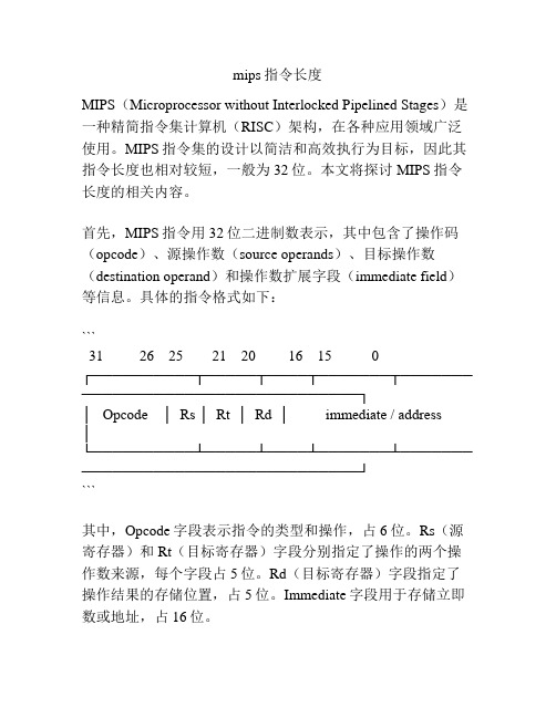
mips指令长度MIPS(Microprocessor without Interlocked Pipelined Stages)是一种精简指令集计算机(RISC)架构,在各种应用领域广泛使用。
MIPS指令集的设计以简洁和高效执行为目标,因此其指令长度也相对较短,一般为32位。
本文将探讨MIPS指令长度的相关内容。
首先,MIPS指令用32位二进制数表示,其中包含了操作码(opcode)、源操作数(source operands)、目标操作数(destination operand)和操作数扩展字段(immediate field)等信息。
具体的指令格式如下:```31 26 25 21 20 16 15 0┌──────────┬─────┬────┬───────┬──────────────────────────────────┐│ Opcode │ Rs │ Rt │ Rd │ immediate / address │└──────────┴─────┴────┴───────┴──────────────────────────────────┘```其中,Opcode字段表示指令的类型和操作,占6位。
Rs(源寄存器)和Rt(目标寄存器)字段分别指定了操作的两个操作数来源,每个字段占5位。
Rd(目标寄存器)字段指定了操作结果的存储位置,占5位。
Immediate字段用于存储立即数或地址,占16位。
根据MIPS指令集架构的设计原则,指令长度一般为32位,这是因为32位的指令长度能够满足大多数指令的需求,同时保持指令处理的高效性。
相比之下,较长的指令长度将导致更高的存储和带宽需求,降低了指令处理的效率;而较短的指令长度则可能限制指令的表达能力。
因此,32位的指令长度是在性能和复杂度之间找到的平衡点。
此外,MIPS还采用了三个寄存器作为指令执行的操作数,分别为源操作数寄存器Rs、目标操作数寄存器Rt和存储结果寄存器Rd。
32位软处理器MicroBlaze的体系结构及其应用 (图)

Xilinx公司的MicroBlaze32位软处理器核是业界最快的软处理解决方案。
支持CoreConnect总线的标准外设集合为MicroBlaze设计人员提供了兼容性和重复利用能力。
MicroBlaze处理器运行在150MHz 时钟下,可提供125 D-MIPS的性能,非常适合设计针对网络、电信、数据通信、嵌入式和消费市场的复杂系统。
MicroBlaze的体系结构MicroBlaze就是基于Xilinx公司FPGA的微处理器IP核,利用它和其他外设IP核一起,就可以完成可编程系统芯片(SOPC)的设计。
MicroBlaze处理器是采用RISC架构和哈佛结构的独立32位指令和数据总线,可以全速度执行存储在片上存储器和外部存储器中的程序并访问其中的数据。
其内核结构如图1所示。
● 内部结构MicroBlaze内部有32个32位通用寄存器和2个32位特殊寄存器——PC指针和MSR状态标志寄存器。
为了提高性能,MicroBlaze还具有指令和数据缓存。
所有的指令字长都是32位,有三个操作数和两种寻址模式。
指令按功能划分有逻辑运算、算术运算、分支、存储器读/写和特殊指令等。
指令执行的流水线是并行流水线,它分为3级流水:取指、译码和执行。
CoreConnect技术CoreConnect是由IBM开发的片上总线通信链,它使多个源的芯片核相互连接成为一个完整的新芯片成为可能。
CoreConnect技术使整合变得更为容易,而且在标准产品平台设计中处理器、系统以及外围的核可以重复使用,以达到更高的整体系统性能。
CoreConnect总线架构包括处理器本机总线(PLB)、片上外围总线(OPB)、一个总线桥、两个判优器,以及一个设备控制寄存器(DCR)总线,CoreConnect总线架构如图4所示。
Xilinx将为所有嵌入式处理器用户提供IBM CoreConnect许可,因为它是所有Xilinx嵌入式处理器设计的基础。
mips 32位 数学运算

mips 32位数学运算
MIPS(Microprocessor without Interlocked Pipeline Stages)是一种常见的32位微处理器架构,常被用于嵌入式系统和一些大型计算机系统中。
MIPS架构提供了丰富的数学运算指令集,包括整数运算、浮点运算等。
在MIPS架构中,整数运算指令包括加法、减法、乘法、除法等基本运算,这些指令可以对寄存器中的数据进行操作,同时还有移位指令用于实现乘除运算。
此外,MIPS还提供了逻辑运算指令,如与、或、非、异或等,用于处理逻辑运算。
在浮点运算方面,MIPS架构提供了丰富的浮点运算指令集,包括浮点加减、乘除、开方、取整等指令,这些指令可以对浮点数进行高精度的运算。
MIPS还支持浮点数和整数之间的转换指令,方便在不同数据类型之间进行转换和运算。
除了基本的数学运算指令外,MIPS还提供了一些高级的数学运算指令,如乘累加指令(MAC)、乘累减指令(MSUB)等,这些指令可以实现复杂的数学运算,提高运算效率。
总的来说,MIPS架构提供了丰富的数学运算指令集,可以满足各种计算需求,同时也提供了一些高级的数学运算指令,方便程序员实现复杂的数学运算。
MIPS架构的数学运算指令集的丰富性和灵活性,使其在嵌入式系统和大型计算机系统中得到了广泛的应用。
MIPS寄存器详解

MIPS 寄存器详解MIPS 有32 个通用寄存器(0?31),各寄存器的功能及汇编程序中使用约定如下:下表描述32 个通用寄存器的别名和用途下面给以详细说明:0:即zero,该寄存器总是返回零,为0 这个有用常数提供了一个简洁的编码形式。
move t0,t1实际为add t0,0,t1 使用伪指令可以简化任务,汇编程序提供了比硬件更丰富的指令集。
1:即at,该寄存器为汇编保留,由于I 型指令的立即数字段只有16 位,在加载大常数时,编译器或汇编程序需要把大常数拆开,然后重新组合到寄存器里。
比如加载一个32 位立即数需要lui(装入高位立即数)和addi 两条指令。
像MIPS 程序拆散和重装大常数由汇编程序来完成,汇编程序必需一个临时寄存器来重组大常数,这也是为汇编保留at 的原因之一。
2..3:(v0?v1)用于子程序的非浮点结果或返回值,对于子程序如何传递参数及如何返回,MIPS 范围有一套约定,堆栈中少数几个位置处的内容装入CPU 寄存器,其相应内存位置保留未做定义,当这两个寄存器不够存放返回值时,编译器通过内存来完成。
4..7:(a0?a3)用来传递前四个参数给子程序,不够的用堆栈。
a0-a3 和v0-v1 以及ra 一起来支持子程序/过程调用,分别用以传递参数,返回结果和存放返回地址。
当需要使用更多的寄存器时,就需要堆栈(stack) 了,MIPS 编译器总是为参数在堆栈中留有空间以防有参数需要存储。
8..15:(t0?t7)临时寄存器,子程序可以使用它们而不用保留。
16..23:(s0?s7)保存寄存器,在过程调用过程中需要保留(被调用者保存和恢复,还包括fp 和ra),MIPS 提供了临时寄存器和保存寄存器,这样就减少了寄存器溢出(spilling,即将不常用的变量放到存储器的过程), 编译器在编译一个叶(leaf)过程(不调用其它过程的过程)的时候,总是在临时寄存器分配完了才使用需要保存的寄存器。
- 1、下载文档前请自行甄别文档内容的完整性,平台不提供额外的编辑、内容补充、找答案等附加服务。
- 2、"仅部分预览"的文档,不可在线预览部分如存在完整性等问题,可反馈申请退款(可完整预览的文档不适用该条件!)。
- 3、如文档侵犯您的权益,请联系客服反馈,我们会尽快为您处理(人工客服工作时间:9:00-18:30)。
32位MIPS处理器说明一、实验目的熟悉现代处理器的基本工作原理;掌握单周期和流水线处理器的设计方法。
二、实验原理及实验内容该32位MIPS处理器主要需要设计ALU、单周期、流水线。
下面分别讲述这三个部分的设计原理及实验内容。
1.ALUALU即算数逻辑单元,要求设计一个32位的ALU,实现基本的算术、逻辑、关系、位与移位运算。
输入32bit的A和B作为操作数,5bit的控制输入ALUFun和一位控制输入Sign,输出32bit的结果Z。
其功能表如下图所示:根据功能表和要求,我们在顶层模块中设计了32bit输入ALUSrc1和ALUSrc2,以及5bit控制ALUFunc,1bit控制Sign,32bit输出ALUOut。
设计了四个主要模块:ALU_ADD_SUB,ALU_CMP,ALU_Logic,ALU_Shift,并根据ALUFunc的值来确定使用的模块。
设计框图思路如下:(1)ALU_ADD_SUB这部分是ALU设计中最重要的一部分。
采用了8位超前进位级联,用与门来实现32位全加器。
减法由加法实现,在运算的开始由ALUFunc判断进行的是加法还是减法,如果是加法则直接将两个操作数输入全加器,最低进位为0,如果是减法则取ALUSrc2的反码之后再做加法运算,最低进位是1。
需要注意的是运算结束之后需要判断结果是否为0(这个在branch指令中尤为重要),是否为负数,还有是否溢出。
是否为溢出还需要检查控制符号,如果控制符号为有效(即有符号计算)则两正数相加得负或两负数相加得正则溢出,溢出则结果符号位反了,再进而判断是否为负。
若为无符号运算,加法结果溢出则最高进位为1,且结果不为负;减法结果溢出等价于结果为负,即最高进位为0。
而结果为0等价于全部位都取0。
(2)ALU_Shift移位运算分别有逻辑左移,逻辑右移,算术右移三种情况。
首先判断是逻辑移位还是算术移位来决定填充0还是填充逻辑位。
之后采取先将操作数根据左移还是右移的判断做出32位扩充,再根据shamt从最高位到最低位判断是否为0来决定取那几位操作数,最后得到移位的结果。
(3)ALU_Logic逻辑运算可以直接按位运算,因此可以直接用A&B、A|B、A^B、~(A|B)计算与、或、异或、或非运算,结果根据ALUFunc的输入用选择器选择即可。
(4)ALU_CMP关系运算需要ALU_ADD_SUB的运算结果作为输入,因为A>B或A<B都可以用A-B的结果是否为负来表示。
通过判断ALU_ADD_SUB的输出是零还是负,即可得知A和B的关系,即:A==B则A-B为0,A!=B则A-B不为0,A<B则A-B 为负,A>=B则A-B不为负,A<=B则A-B为负或为0,A>B则A-B不为负或0。
而A和0的关系也可以同理判断。
只需要知道A-0的正负即可。
2.单周期实验指导书中,模块设计与连接如下(1)CPU_sc时钟clk,reset使能信号rst_n,定时器TL寄存器,Switch,串口接收Uart_Rxd,和三个中断信号IRQ作为输入,定时器TH寄存器,定时器使能信号,七段数码管,串口输出与输出使能,以及LED作为输出。
并在其中调用了所需要的模块:InstructionMemory(指令集),cpucontrol(控制单元),RegFile(寄存器模块),ALU,DataMemory(存储器模块)。
我们在这里实现了PC寻址,首先判断reset是否使能来确定PC取0还是取PC_nxt。
将中断跳转地址分别赋予ILLOP_TIMER,ILLOP_TX和ILLOP_RX,并通过判断三种中断使能标志来确定中断取值。
之后PC_nxt根据PCSrc的控制信号来判断取PC_4(即PC+4)、是否跳转至branch目标地址、jump目标地址、jump Register中的寄存器储存地址、中断目标地址或者异常目标地址,最终完成PC寻址。
这之后我们在设计了寄存器的读写,这里面我们发现了实验指导书中的一处稍微有些争议的地方:实验指导书中的MEMToReg控制信号控制的多路选择器有三种输出选择:计算得出的ALUOut,存储器中读出的ReadData和PC+4,分别对应于大多数指令、lw指令和jal,jalr指令,但是进中断时所存指令选用PC+4是有问题的,因为我们并不能控制走到那条指令的时候进入中断,如果出中断之后从Xp读出的是当前指令的下一条指令,那么当前指令就并未被有效执行。
或者说如果我们选择执行完当前指令再进入中断,那么如果当前是一个branch或者jump指令,那我们出中断之后进入的并不是跳转的对象指令,而是当前指令的下一条指令,branch和jump就等于直接失去了作用,汇编程序就会出不必要的bug。
为了解决这个问题,我们给MEMToReg增加了一条选择,即可以选择PC作为写寄存器的输入。
之后我们设计了DataBusA和DataBusB的输入,根据ALUSrc1和ALUSrc2进行选择,还对立即数的扩展做了处理,判断是有符号扩展还是无符号扩展,计算了branch指令的目标地址,最后判断了允许中断的IRQ信号的取值。
在这里受到我们重视的另一个问题就是对PC[31]的取值。
实验指导书中要求:PC的最高位PC[31]为监督位。
当该位为‘1’时,处理器处于内核态,此时异常和中断被禁止;当该位为‘0’时,处理器处于普通态,此时允许发生中断和异常。
只有RESET、异常、中断等有可能将PC[31]设置为‘1’,其他指令不能设置该位为‘1’,JR和JALR指令可以使监督位清零。
并且PC+4逻辑电路实现时应该保证PC[31]不变,分支语句和J、JAL语句不应该改变PC[31],当执行JR、JALR指令时,PC[31]的值由跳转地址($Ra)中的第31位(最高位)决定。
所以我们在每一次赋值中对PC[31]做了特殊处理,很好地满足了上述要求。
(2)InstructionMemory输入address,输出指令,其内容为我们的汇编代码,这段代码将在之后进行阐述。
(3)cpucontrol为了更好地看清每一条指令对控制信号的需求我们做了一个真值表来记录各指令功能、用法及对应的控制信号。
其中我们在汇编中用了ori指令,所以在指令集里多增加了这条指令以方便我们更好地完成汇编。
其中我们特别注意了对PC[31]的判断,以确定什么时候是中断或异常指令,什么时候不能有中断异常指令。
(4)RegFile我们并没有用老师提供的regfile文件而是自己又重新写了一个。
输入时钟、reset使能信号、read address A、read address B、write address C、需要写入寄存器的值和寄存器写控制信号,输出从A中读出的data和从中读出的data。
先找出需要写入的寄存器,再找出需要读出的寄存器。
整体来看对于我们而言要更加清晰一些,并且特别设计了0寄存器始终为0。
(5)ALU之前已经有过阐述。
(6)DataMemory在DataMemory中,我们把RAM分成了两部分,一部分为dataRAM,256字,一部分为PeripheralRAM即外设RAM。
之后分别实现写RAM和读RAM。
写RAM中,通过判断地址前24位的取值来决定是写data还是写外设,因为写外设只发生在中断部分,而中断部分的最明显特征即为地址开始位为4。
同时对flag标志信号和使能信号进行更改。
读地址过程中我们同样是通过判断地址前24位的取值来决定是读data还是读外设。
这样就综合了原本的DataMemory和Peripheral,让代码更为拥有整体性。
(7)MCU_sc这部分调用了单周期的CPU_sc,串口UART,定时器Timer,和七段数码管扫描digitube_scan,可以输出硬件显示,是严格意义上的顶层模块,然而并不是cpu整体构造的重点。
在其中为了能够让我们设计的单周期cpu正常工作,对时钟进行了二分频。
(8)UART使用的是朱宸卓当时实验的串口程序,并按照需求进行了简单的修改。
我们对串口选择中断访问。
(9)TIMER定时器TIMER按照实验指导书上的说明设置了一个从hffffffff计时到全1的定时器。
以满足我们对扫描频率的要求。
(10)digitube_scan使用的是老师提供的digitube_scan文件。
3.流水流水线的设计中,需要将整个过程分为取指令(IF)、指令译码(ID)、执行(EX)、数据访问(ME)、写回(WB)五个部分,我们设计的流水基本采用此模块设计连接思想:其中InstructionMemory,DataMemory、RegFile、cpucontrol和ALU与单周期没有任何区别。
(1)CPU_ppl与单周期类似,在这里我们同样要完成PC寻址过程,同时还要完成从IF/ID到ID/EX,再到EX/MEM,再到MEM/WB的逐级保存,在时钟的上升沿都使它们等于对应的nxt信号。
之后根据控制信号完成每一个nxt指令的赋值,并在其中解决forwarding,stall和flush对四个寄存器赋值的影响。
这一点我们会在forwarding和hazard部分进行阐述。
我们还做了一个小的ALU比较器,因为我们的程序中把所有的branch都做了提前,所以需要提前知道branch的比较结果,这个ALU实现十分简单,所以并不会造成太大延时。
下面需要比较详细阐述的是我们对forwarding和hazard的解决方案。
(2)Forwarding我们首先解决的便是书上的那两条转发情况:如果要读的寄存器的值还未被写入,则提前对计算得出的值进行转发,其中受到影响的分别是EXMEM_RegisterRd和IDEX_RegisterRs、Rt以及MEMWB_RegisterRd和IDEX_RegisterRs、Rt,分别对应于ForwardA和ForwardB。
但我们发现书上的这两种情况并不够用。
如果下一条指令需要存入RAM的数据是上一条指令才写入寄存器的,则需要转发。
对应于ForwardC.如果是branch或者jr指令,因为我们在流水中对这两类指令做了提前处理,使它们在ID阶段就能够知道自己是否跳转或者跳转到哪里,这样会遇到上一条指令刚刚计算得出的数据还没有存入寄存器就需要被branch或jr在ID阶段使用,则需要一次转发。
对应于ForwardD和ForwardE。
这样转发单元才趋于完整。
(3)Hazard遇到hazard我们一共采取了两种解决方案:stall和flush。
并且也尽可能全面地考虑了hazard的情况。
首先是书上提到的lw冒险,当lw与下一条指令产生关联,即lw取出的指令在下一条寄存器中需要使用时,需要阻塞一个周期以完成从内存中取data,并将ID寄存器flush以清空指令和控制信号。