吸波材料0.15MM规格书英文版
OFSPower Over Fiber产品说明书
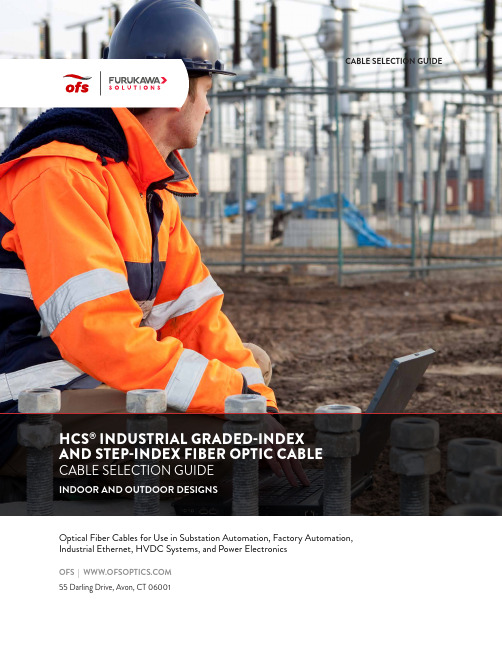
CABLE SELECTION GUIDEHCS ® INDUSTRIAL GRADED-INDEX AND STEP-INDEX FIBER OPTIC CABLEOFS | 55 Darling Drive, Avon, CT 06001CABLE SELECTION GUIDEINDOOR AND OUTDOOR DESIGNSOptical Fiber Cables for Use in Substation Automation, Factory Automation, Industrial Ethernet, HVDC Systems, and Power ElectronicsHCS ® INDUSTRIAL GRADED-INDEX AND STEP-INDEX FIBER OPTIC CABLECABLE SELECTION GUIDEW W W.O F S O P T I C S.C O MWhy HCS and GiHCS ®?200 μm Step-Index Hard Clad Silica62.5 μm OM1 Graded-Index Hard Clad Silica • Wide operating temperature range• Resistant to abrasion, vibration, and industrial chemicals• HCS extends the distance and bandwidth of POF (Plastic Optical Fiber) Systems • Superior crush, twist, tensile strength, and flex performance• Ideal for Broadcom Versatile Link, Industrial Ethernet, Fieldbus, and Power over Fiber (PoF)• Suitable for indoor and outdoor use62.5 µmPictureC210582.2 mmLSZH Simplex22 mm5 lbs (22.2 N)ST, SMA, V-Pin, LC BC04265-10 2.2 mm PVC Simplex 22 mm5 lbs (22.2 N)ST, SMA, V-Pin, LC AC01281-10 2.5 mm PVC Simplex 25 mm55 lbs (244.7 N)ST, SMAC21050 2.5 mm LSZH Simplex 25 mm 55 lbs (244.7 N)ST, SMA HCS ® INDUSTRIAL GRADED-INDEX AND STEP-INDEX FIBER OPTIC CABLE CABLE SELECTION GUIDEW W W.O F S O P T I C S.C OMHCS ® INDUSTRIAL GRADED-INDEX AND STEP-INDEX FIBER OPTIC CABLECABLE SELECTION GUIDEThe cables in this brochure are intended to be used with OFS Crimp & Cleave field termination connectors andtermination kits.PictureC210608.0 mm (2.2 mm Subs) LSZH 2-Fiber Breakout 80 mm 45 lbs (200.2 N)ST, SMA, V-Pin, LC C210639.5 mm (2.2 mm Subs)LSZH 2-Fiber Glass Armor 95 mm 200 lbs (889.6 N)ST, SMA, V-Pin, LC C210528.0 mm (2.5 mm subs) LSZH 2-Fiber Breakout 80 mm 155 lbs (689.5 N)ST, SMAFor additional information please contact your sales representative.You can also visit our website at or call 1-888-fiberhelp (1-888-342-3743) USA or 1-770-798-5555 outside the USA.。
吸波材料英文

吸波材料英文Absorbing materials, also known as absorbers, are materials that can effectively absorb and attenuate electromagnetic waves, sound waves, or other types of waves. These materials are widely used in various fields, including electronics, telecommunications, construction, and aerospace. In this document, we will focus on absorbing materials for electromagnetic waves, also known as electromagnetic wave absorbers.Electromagnetic wave absorbers are materials designed to absorb electromagnetic radiation, such as microwaves, radio waves, and infrared waves. They are used to reduce the reflection and transmission of electromagnetic waves, thereby minimizing interference and improving the performance of electronic devices and systems.There are various types of electromagnetic wave absorbers, each with its own unique properties and applications. The most common types include magnetic absorbers, dielectric absorbers, and hybrid absorbers. Magnetic absorbers are made of magnetic materials, such as ferrites, and are effective at absorbing low-frequency electromagnetic waves. Dielectric absorbers, on the other hand, are made of dielectric materials, such as carbon or metal-loaded polymers, and are effective at absorbing high-frequency electromagnetic waves. Hybrid absorbers combine the properties of both magnetic and dielectric materials to achieve a broader absorption bandwidth.The design and development of electromagnetic wave absorbers require careful consideration of factors such as the operating frequency, absorption bandwidth, thickness, weight, and environmental stability. In addition, the fabrication process, cost, and scalability are also important considerations. Researchers and engineers are constantly exploring new materials and technologies to improve the performance and efficiency of electromagnetic wave absorbers.In recent years, there has been growing interest in the development of lightweight, flexible, and tunable electromagnetic wave absorbers. These absorbers are particularly important for applications in wearable electronics, flexible displays, and aerospace systems. By using advanced materials and design techniques, researchers have been ableto create absorbers that are not only highly efficient at absorbing electromagnetic waves but also have additional functionalities, such as mechanical flexibility and tunable absorption properties.In conclusion, absorbing materials for electromagnetic waves play a crucial role in various technological applications. The ongoing research and development in this field continue to drive the advancement of electromagnetic wave absorbers, leading to improved performance, reduced interference, and enhanced functionality in electronic devices and systems. As the demand for wireless communication, IoT devices, and 5G technology continues to grow, the development of advanced electromagnetic wave absorbers will be essential for meeting the evolving needs of the modern world.。
丽智电阻规格书
CR 0805
J
8
0472
G
Series Name Product.. CR=Chip Resistor
Size Code 0201 0402 0603
Tolerance B=± 0.1% C=± 0.25% D=± 0.5%
Power Rating 1= 1W 2= 1/2W 2= 3/4W (for 2010) 3= 1/3W
Standard Resistance Values
CR0402
CR0603 CR0805
±0.5%
D
10~1M
E96
CR1206
CR0201
±Hale Waihona Puke %FCR0402±2%
G
1R0-10M 0R (jumper)
E96
CR0603
±5%
J
CR0805
±10%
K
1R0~22M
CR1206 CR1210
0R (jumper) (0201:1R0-10M)
digits. Example as following:
“ 331 ”indicates that it is 0603 ±1% 330ohm product.
3.Rating
3.1 Rated Power (%)
Rated power shall be load power corresponding to normal wattage suitable for
Example: 330 ohm: 0331, 4.7K ohm: 0472
22K ohm: 0223, 100K ohm: 0104
2
文件編號:613-00-001 版本:V15.0
Spartan Scientific APVS15产品说明书

86Air Piloted 2-Way Media Separated ValveSeries APVS15Dimensional DataThe Spartan Scientific APVS15 is an inert gas/spring operated, Single Acting Normally Closed, or Double Acting media compatible dia -phragm valve designed for control of high purity, aggressive and corrosive liquid chemical media. With a small overall footprint, and low dead volume, the APVS15 features CPVC bodies, and FKM, EDPM and NBR elastomers to control orifice sizes 16mm and 20mm which afford Cv ratings of 4.70 and 10.9 that far exceed competitive valves of this type. Pressure ratings go from 10 to 100 psi depending on orifice size and each valve is tested to bubble tight standard ANSI FCI 70-2 Class VI. The APVS15 can be controlled by our proven Spartan Scientific 3-way solenoid pilot valve which enhances operation with manual override and indicator lighted connector options. The Normally Closed version features an optical position indicator showing valve open condition. The APVS15 is used where sampling, drain -ing, or transferring process fluid are performed. A Normally Open version can be made using a Normally Open pilot valve. In the case of pilot gas failure, the valve will fail closed. In the case where electric power is lost but pilot gas remains, the valve will remain open. An optional magnetic piston is available for end of stroke sensing when combined with the additional valve position sensor.ALL DIMENSIONS ARE IN INCHES UNLESS OTHERWISE NOTEDA56-2240 Rev.03Non-Piloted Version0.81GROOVEAIR PILOTEDAPVS15 - 2 8 - DOrder Example: APVS15-1Q028-DAD7AFKM, 16mm Orifice size,No magnetic piston, 2-way N.C.,1/2” NPT, 120 VAC 50/60 Hz, DIN Spade Function:Single Acting Normally Closed; or Double Acting,Air Piloted, media separated diaphragm valvePort Size:1/2” NPT3/4” NPT(Others available on request)Orifice Sizes / 16mm / 4.70 CvFlow Factor: 20mm / 10.9 CvPressure Range:10 to 100 psiPilot Pressure Range: 60 to 100 psi(depending on orifice size)Temp. Range: Fluid Max.: +60°CDry Range: Ambient +10°C to +50°CMedia:All fluids and gases compatible with wetted materialsMounting: (2x) 1/4” - 20 UNC Tapped Holes, 0.5” DP. On pipeWetted Materials:Valve Body: CPVC (Others available on request)Elastomers: FKM, NBR, EPDM,Pilot Option Function: 3-Way, 2-Postion; Direct Acting;Normally Closed, Normally OpenPressure Range: 60 to 100 PSIPort Size: 1/8” NPTCoil Data:Duty Cycle: Continuous (within specifications)Encapsulation: Glass-Filled NylonInsulation: Class FPower Rating: 6.5 Watts8.5 VAVoltage: 12, 24, 120 VDC120, 220, 240 VAC 50/60 HzVoltage Tolerance: +/- 10% NominalWinding: Class HConnections:Spades: Terminals AMP 6.3x0.8 width 11mm(Available in DIN Style “A” EN175301-803for 3.0mm orifice or larger)Flying Lead: PVC 22 AWG, Multi-Strand Copper Wire,300V, 12” minimum lengthPackaged Weight: Piloted: 1.72 lbs.Non-piloted: 1.5 lbs.Additional OptionsValve Position Sensor Order Part No.:Electronic PNP9ft PVC cable9E76-000-0318mm quick connect9E76-000-331Electronic NPN9ft PVC cable9E76-000-0328mm quick connect9E76-000-332Reed SPST9ft PVC cable9E76-000-0028mm quick connect9E76-000-302Sensor Mating Cordsets Order Part No.:8mm Quick Connect2 meter female3 pin RC08-AFM030-0120CB0A5 meter female 3 pin RC08-AFM030-0150CB0APilot Valve Lighted Connector Order Part No.:6ft PVC Cable, Ground DownPilot Options 2, A - 12VDC5J560-201-US0APilot Options 3, B - 24VDC5J560-201-US0APilot Options 4, C - 120VDC5J560-501-US0APilot Options 7, F - 120VAC5J560-501-US0APilot Options 8, G - 220VAC5J560-801-US0APilot Options 9, H - 240VAC5J560-801-US0AAIRPILOTED87。
cst吸波材料参数

cst吸波材料参数CST吸波材料(Complexed Sticky Tape)主要用于电磁波吸波,是一种以热塑性弹性体为基材,通过添加吸波材料和粘合剂进行复合制备的材料。
CST吸波材料具有很好的吸波性能,可以在广泛的频率范围内将电磁波吸收到自身内部而减少反射。
CST吸波材料的性能参数主要包括吸波性能、工作频率范围、厚度、机械性能和耐候性等。
下面将详细介绍各项参数:1.吸波性能:CST吸波材料的主要功能是吸收电磁波,减少反射。
吸波性能的表征指标是吸波率(Absorption coefficient)和吸波带宽(Absorption bandwidth)。
吸波率是指材料吸收的电磁波功率占入射功率的比值,数值在0到1之间。
吸波带宽是指材料能够有效吸收电磁波的频率范围,通常以-10dB的吸收率为界限。
2.工作频率范围:CST吸波材料的工作频率范围取决于吸波材料的成分和结构。
不同的吸波材料有不同的吸波频率范围,常见的频率范围从几十兆赫兹到几千兆赫兹。
在工程应用中,选择合适的吸波材料要根据具体的工作频率范围来确定。
3.厚度:CST吸波材料的厚度是影响材料吸波性能的重要因素。
一般来说,材料的厚度越大,吸波性能越好,但同时也会增加材料的重量和成本。
根据具体的应用需求,可以选择合适的厚度。
常用的CST 吸波材料厚度从几毫米到几厘米不等。
4.机械性能:CST吸波材料除了具有良好的吸波性能外,还需要具备一定的机械性能以满足实际应用需求。
机械性能包括材料的拉伸强度、弯曲强度、抗冲击性等。
一般来说,CST吸波材料应具备足够的强度和韧性,以保证材料在使用过程中不会发生断裂或损坏。
5.耐候性:CST吸波材料通常在室外环境中使用,所以需要具备一定的耐候性能。
耐候性是指材料在长时间暴露于自然环境中,不会因为氧化、紫外线辐射、温湿度变化等因素而导致性能衰减。
耐候性能好的CST吸波材料可以保证吸波性能的长期稳定性。
总之,CST吸波材料是一种广泛应用于电磁波吸波领域的材料,其主要性能参数包括吸波性能、工作频率范围、厚度、机械性能和耐候性等。
吸波材料参数
吸波材料参数吸波材料是一种能够有效吸收电磁波能量的材料,广泛应用于电磁兼容、无线通信、雷达隐身等领域。
吸波材料的性能参数对其吸波性能有着重要影响,下面将对吸波材料的参数进行详细介绍。
1. 工作频率范围。
吸波材料的工作频率范围是指其能够有效吸收电磁波的频率范围。
通常来说,吸波材料的工作频率范围越宽,其在不同频段的吸波性能就越好。
因此,选择吸波材料时需要根据实际应用的频率范围来进行合理选择。
2. 吸波性能。
吸波性能是评价吸波材料性能的重要参数,通常用反射损耗和吸收损耗来描述。
反射损耗是指电磁波在材料表面的反射损耗,吸收损耗是指电磁波在材料内部的吸收损耗。
一般来说,吸波材料的反射损耗和吸收损耗越大,其吸波性能就越好。
3. 厚度。
吸波材料的厚度对其吸波性能有着重要影响。
一般来说,吸波材料的厚度越大,其在低频段的吸波性能就越好,而在高频段的吸波性能则会受到影响。
因此,在实际应用中需要根据具体频率范围和吸波要求来选择合适的厚度。
4. 温度稳定性。
吸波材料的温度稳定性是指其在不同温度下的吸波性能稳定程度。
一般来说,吸波材料的温度稳定性越好,其在复杂环境下的吸波性能就越可靠。
因此,在一些特殊应用场景中,需要选择具有良好温度稳定性的吸波材料。
5. 加工性能。
吸波材料的加工性能对其在实际应用中的加工和成型有着重要影响。
良好的加工性能能够保证吸波材料在成型过程中不会出现裂纹、气泡等缺陷,从而保证其吸波性能。
因此,在选择吸波材料时需要兼顾其加工性能。
综上所述,吸波材料的参数包括工作频率范围、吸波性能、厚度、温度稳定性和加工性能等。
合理选择吸波材料的参数,能够有效提高其在电磁兼容、无线通信、雷达隐身等领域的应用性能,为相关领域的发展提供有力支持。
CPC1020N;中文规格书,Datasheet资料

0.6
0.5
0.4 -40 -20
IF=5mA
0 20 40 60 Temperature (ºC)
80 100
LED Forward Voltage (V)
LED Forward Current (mA)
*The Performance data shown in the graphs above is typical of device performance. For guaranteed parameters not indicated in the written specifications, please contact our application department.
0.20
(IL=1A)
0.18
0.16
0.14
0.12
0.10
0.08 -40 -20
0 20 40 60 Temperature (ºC)
80 100
Turn-On Time (ms)
Typical Turn-On Time vs. Temperature (IL=100mA)
3.5
3.0
2.5
2.0
Device Count (N)
Typical On-Resistance Distribution
(N=50, I =2mA, I =1A, T =25ºC)
F
L
A
20
15
10
5
0 0.113 0.114 0.115 0.116 0.117 0.118
On-Resistance (Ω)
Typical IF for Switch Operation (N=50, IL=100mA, TA=25ºC)
7D CPT 规格书--普厚

TFT LCD Preliminary Specification Model Name :CLAP070LF01CWCustomer:___________________________ Approved by:_________________________Note: 1. Please contact HDC Display Corp. before designing your product based on this module specification.2.The information contained herein is presented merelyto indicate the characteristics andperformance of ourproducts. No responsibility is assumed by HDC foranyintellectual property claims or other problems thatmay result from application based onthe moduledescribed hereinApproved By ASSEMBLY LCD TV DivisionR&D DEPT.QA Dept Checked byTV LCM Marketing and Sale Dept ReviewedRev. Date Description of change1.0 2010/9/26 Preliminary Product Specification was first issued.CONTENTS,1.0 General description. ……………………………...... p.12.0 Absolute maximum ratings …………………….….. p.3………………..….. p.43.0 ELECTRICAL CHARACTERISTICS………….……… p.54.0 INTERFACE PIN CONNECTION5.0 O PTICAL CHARACTERISTICS ….…….………. p.66.0 RELIABILITY TEST ITEMS….…….……….………. p.7…………………………….….… p.97.0 LOT MARK8.0 Outline dimension …………………………….……. p.14……………………………………. p.169.0 Package specification10.0 General precaution ……………………………….... p.171.0 OVERVIEWCLAP070LF01CW is 7.0" color TFT-LCD (Thin Film Transistor Liquid Crystal Display) OLB module (finish outer lead bonding) composed of LCD panel and driver ICs (the backlight is not included in this OLB module).The 7.0" screen produces 800(*3)X480 resolution image. By applying R.G.B. input signal,full color images are displayed.General specifications are summarized in the following table:ItemSpecification Unit Outline Dimension 164.9 x 100 x 5.7(Typ.)mm Display area 153.6(H) x 86.64(V) mm Number of Pixel 800 (H) x 3RGB x 480 (V) pixels Pixel pitch 0.1926(H) x0.1975(V) mm Pixel arrangement RGB Vertical stripe Display mode Normally whiteNunber of color 16.2MResponse Timr(Tr+Tf) 25ms(typ.) g Panel Transmittance(%) 5.1(typ)Power Consumption(W) 327Mw(typ) Surface TreatmentAnti-Glare, Hardness:3HWSHENZHEN HUIPUCHUANGXIN TECHNOLOGY CO., LTD2. ABSOLUTE MAXIMUM RATINGS2.1. TFT LCD ModuleItemSymbol Min. Max. Unit NoteDigital Supply Voltage DVDD-0.3 +0.5 V Analog Supply Voltage AVDD-0.5+13.5 V Gate On Voltage VDDG -0.3 +42 V Gate Off Voltage VEEG -20 +0.3 V Gate On-Gate Off VoltageVDDG-VEEG 12 40 VOperation Temperature T op -20 70 ℃ Note 1 Storage TemperatureT stg-3080℃Note 1Note1:If users use the product out off the environmemtal operation range (temperature and humidity ),it will have visual quality concerns.2.2 Back-Light UnitThe back-light system is an edge-lighting type with 21 LED. The characteristic of the LED is shown in the following tables.Item Symbol Typ. Max. Unit NoteLED currentI 100 - mA (1) (2)(3) LED voltageV 9.6 11 V (1) (2)(3)3. ELECTRICAL CHARACTERISTICSItemSymbolMin Min Typ Max. Unit Note Digital Supply Voltage DVDD 3 3.3 3.6 V Analog Supply Voltage AVDD 9.4 9.6 9.8 VGate On Voltage VDDG -17 18 19 V Gate Off Voltage VEEG -6.6 -6 -5.4 V Common Voltage VCOM 3.8 4 4.2 V Note1 VIH 0.7D VDD - DVDD V Logic Input VoltageVILGND-0.3DVDDVNote1:Please adjust VCOM to make the flicker level be minimum.3.1 Current consumptionNote Item Symbol Condition Min.Typ Max. UnitGate on Current IVDDG VDDG =18 V- 0.5 1 mA Note1 Gate off Current IVEEG VEEG= -6 V- 0.5 1 mA Note1- 8 15 mA Note1 Digital Current IDVDD DVDD =3.3V- 30 40 mA Note1 Analog Current IAVDD AVDD = 9.2VTotal PowerPC- - 327 458 mw Note1 ConsumptionNote1: Typ. specification:Gray-level test PatternMax. specification:Black test Pattern3.2 Power、Signal sequencePower On:DVDD→AVDD/VEEG→VDDG→Video &Logic SignalPower Off:Video &Logic Signal→VDDG→AVDD/VEEG→DVDD0<T1≦10ms T5>0ms T3>10ms 0<T7≦10msT2>20ms T6>0ms T4>0ms 0<T8≦10ms3.3 Timing characteristics of input signalsITEMS Y M B O L M I N . T Y P . M A X .U N IT N o te Dot Clock 1/t CLK 29 33 38 MHZDCLKDCLK pulse duty Tcwh 40 50 60 %Setup TimeTesu 8 ns Hold timeTehd 8 ns Horizontal Period t H 1026 1056 1086t CLKHorizontal Valid t HA 800 t CLK Horizontal Blank t HB - 256 - t CLK Vertical Period t V 515 525 535 ThVertical Valid t VA 480 Th DEVertical Blank T vb - 45 - Th HSYNC Setup Time Thst 8 - t CLK HSYNC Hold Time Thhd 8 - - t CLK VSYNC Setup Time Tvst 8 - - t CLK VSYNC Hold Time Tvhd 8 - - t CLK Horizontal Period th 1026 1056 1086t CLK Horizontal PulseWidth thpw - 30 - t CLK thb + thpw=46DCLKisfixed Horizontal Back Porch thb - 16 - t CLKHorizontal Front Porchthfp 180 210 340 t CLK Horizontal Valid thd 800 t CLK Vertical Period tv 515 525 535 thVertical Pulse Width tvpw 13 th Vertical Back Porch tvb 10 th tvpw + tvb = 23th isfixedVertical Front Porchtvfp 12 22 32 thSYNCVertical Validtvd 480 thSetup TimeTdsu 8 - - ns DATA Hold TimeTdhd8 - -Ns4. INTERFACE PIN CONNECTION4.1 CN1(Signal of interface)Pin NO.Symbol DESCRIPTION1 V LED+Power for LED backlight (Anode)2 V LED+Power for LED backlight (Anode)3 V LED Power for LED backlight (Cathode)4 V LED Power for LED backlight (Cathode)5 GND Power ground6 VCOM Common Voltage7 DVDD Digital Power8 MODE DE/SYNC mode select. Normally pull highH: DE mode. L: HSD/VSD mode9 DE Data Enable signal10 VSD Vertical sync input. Negative polarity11 HSD Horizontal sync input. Negative polarity12 B7Blue Data Input13 B6Blue Data Input14 B5Blue Data Input15 B4 Blue Data Input16 B3 Blue Data Input17 B2 Blue Data Input18 B1 Blue Data Input29 B0 Blue Data Input (LSB)20 G7 Green Data Input(MSB)21 G6 Green Data Input22 G5 Green Data Input23 G4 Green Data Input24 G3 Green Data Input25 G2 Green Data Input26 G1 Green Data Input27 G0 Green Data Input(LSB)28 R7 Red Data Input(MSB)39 R6 Red Data Input30 R5 Red Data Input31 R4 Red Data Input32 R3 Red Data Input33 R2 Red Data Input34 R1 Red Data Input35 R0 Red Data Input(LSB)36 GND Power ground37 DCLK Clock input38 GND Power ground39 SHLR Left or Right Display Control40 UPDN Up / Down Display Control41 VDDG Positive Power for TFT42 VEEG Negative Power for TFT43 AVDD Analog Power44 RSTB Global reset pin. Active low to enter reset state.Suggest to connecting with an RC reset circuit for stability.Normally pull high. (R=10KΩ,C=1μF)45 NC Not connect46 VCOM Common Voltage47 DITH Dithering settingDITH=”H” 6bit resolution(last 2 bit of input data truncated)DITH=”L” 8bit resolution(default setting)48 GND Power ground49 NC Not connect50 NC Not connect;5. OPTICAL CHARACTERISTICS ( Use CPT LED backlight )Note 1: Definition of Response Time.(White-Black)The response time is defined as the time interval between the 10% and 90% amplitudes.ItemSymbol ConditionMin.Typ.Max. Unit NoteTransmittance T 4.8 5.1 - %- -Response timeT R +T F25 35msec 1 Center Luminance ofWhiteL C 90 105 -cd/m 2Horizontalφ120140 - . 2Viewing 2 AngleVerticalθPoint-5CR ≧10100120.. 2W x 0.260 0.32 0.360 Color chromaticity (CIE1931)WhiteWyθ=φ ﹦0°0.270.3300.370(3)6. RELIABILITY TEST ITEMSNo Item Conditions1 High Temperature Storage a=+80o C, 240hrs2 Low Temperature Storage Ta=-30o C, 240hrs3 High Temperature Operation Ta=+70o C, 240hrs4 Low Temperature Operation Ta=-20o C, 240hrs5 High Temperature and High Humidity(Operating)Ta=+60o C, 90%RH, 240hrs6 Thermal Cycling Test (non operation)-30oC(0.5hr)->0oC(0.5hr), 200cycles7 Packing1. Sine, 1.5G, 5~200Hz, 1hr X,Y,Zdirection2. Random, 1.5Grms, 5~200Hz, 15min/X,Y,Z direction3. Half-Sine, 70G, 11ms+ X axis, 2 Times4. Half-Sine, 200G, 2ms+ X axis, 2 Times5. 90 degree topple to dash against thehard- face of table.8 Altitude Test (non operation)50000ft, 24hr (25℃)9 Altitude Test (operation)10000ft, 02hr (25℃)10 Pressure cooker Test121℃100%R.H., 2atm, 16hr/20hr11 Electrostatic Discharge± 200V, 200pF,07.LOT MARK7. 1 product label7. 2 Out box label8. OUTLINE DIMENSION9. PACKAGE SPECIFICATION9.1 Packing assembly drawings10. GENERAL PRECAUTION10.1 Use RestrictionThis product is not authorized for use in life supporting systems, aircraft navigation control systems, military systems and any other application where performance failure could belife threatening or otherwise catastrophic.10.2 Disassembling or ModificationDo not disassemble or modify the module. It may damage sensitive parts inside LCDmodule, and may cause scratches or dust on the display. HannStar does not warrantthe module, if customers disassemble or modify the module.10.3 Breakage of LCD Panel10.3.1.If LCD panel is broken and liquid crystal spills out, do not ingest or inhale liquidcrystal, and do not contact liquid crystal with skin.10.3.2. If liquid crystal contacts mouth or eyes, rinse out with water immediately.10.3.3. If liquid crystal contacts skin or cloths, wash it off immediately with alcohol andrinse thoroughly with water.10.3.4. Handle carefully with chips of glass that may cause injury, when the glass isbroken.10.4 Electric Shock10.4.1. Disconnect power supply before handling LCD module.10.4.2. Do not pull or fold the LED cable.10.4.3. Do not touch the parts inside LCD modules and the fluorescent LED’s connectoror cables in order to prevent electric shock.10.5 Absolute Maximum Ratings and Power Protection Circuit10.5.1. Do not exceed the absolute maximum rating values, such as the supply voltagevariation, input voltage variation, variation in parts’ parameters, environmentaltemperature, etc., otherwise LCD module may be damaged.10.5.2. Please do not leave LCD module in the environment of high humidity and hightemperature for a long time.10.5.3. It’s recommended to employ protection circuit for power supply.10.6 Operation10.6.1 Do not touch, push or rub the polarizer with anything harder than HB pencil lead.10.6.2 Use fingerstalls of soft gloves in order to keep clean display quality, when personshandle the LCD module for incoming inspection or assembly.10.6.3 When the surface is dusty, please wipe gently with absorbent cotton or other softmaterial.10.6.4 Wipe off saliva or water drops as soon as possible. If saliva or water drops contactwith polarizer for a long time, they may causes deformation or color fading.10.6.5 When cleaning the adhesives, please use absorbent cotton wetted with a littlepetroleum benzine or other adequate solvent.10.7 Static Electricity10.7.1 Protection film must remove very slowly from the surface of LCD module toprevent from electrostatic occurrence.10.7.2. Because LCD module use CMOS-IC on circuit board and TFT-LCD panel, it is veryweak to electrostatic discharge. Please be careful with electrostatic discharge.Persons who handle the module should be grounded through adequatemethods.10.8 Strong Light ExposureThe module shall not be exposed under strong light such as direct sunlight. Otherwise,display characteristics may be changed.10.9 DisposalWhen disposing LCD module, obey the local environmental regulations.SHENZHEN HUIPUCHUANGXIN TECHNOLOGY CO., LTD。
- 1、下载文档前请自行甄别文档内容的完整性,平台不提供额外的编辑、内容补充、找答案等附加服务。
- 2、"仅部分预览"的文档,不可在线预览部分如存在完整性等问题,可反馈申请退款(可完整预览的文档不适用该条件!)。
- 3、如文档侵犯您的权益,请联系客服反馈,我们会尽快为您处理(人工客服工作时间:9:00-18:30)。
3.Material Data
item Magnetic Absorber Material Flexibale soft+Resin+Polymer
4. Characteristics
Properties
Absorber Sheet Tensile Strength Relative μ' Operating Temp. Surface Resistance Gravity Appl. Frequency Dielectric Strength(DC) Themal Cond. Adhesion Strength Thickness Flame Retardant RoHSຫໍສະໝຸດ Typical Value
Polymer 4.6Mpa 30 "-25~85"℃ 1.6*105Ω 3.4g/cm3 500MHz~8GHz 400V 0.6W/mK >1.0 kgf/inch 0.15mm meet UL-94V0 RoHS Compliance & PVC-free 5mm(0.1mA/1mA leakage)
Typical 5mm(0.1mA/1mA leakage) ASTM D 5470 ASTM D 1000
liance & PVC-free
ets or rolls in bags before put into cartons.
or sun exposure.
urpose and specific aplliciation method.
材 料 有 限 公 司 ODUCTS CO.,LTD
Magnetic Absorber
Absorber Sheet Non-conductive PSA Release Liner
Thickness 0.15mm
Test Method
N/A ASTM D 1000 1MHz Long time Typical
7.The above data is obtained in the average after several tests.
The user must determine whether the product is suitable for a particular purpose and specific aplliciation method.
5. Packing:
Magnetic Absorbers are to be wrapped in shrink film, then pakced by sheets or rolls in bags before put into cartons.
6.stock and QA:
The product should stay in shade to avoid high tempreture, high humidity or sun exposure. In this case, it comes with a period of 6 months warraty.
ng Town, Bao'an District, , China 518103
Emai: hfc_zjl@
C Bidg, 3rd Industrial Park, Fenghuang Fuyong Town, Bao'an District, Shenzhen City, Guangdong Province, China 518103
TEL:0086 755-27306187 FAX:0086 755-27306260 Emai: hfc_zjl@
深 圳 市 鸿 富 诚 屏 蔽 材 料 有 限 公 司 SHENZHEN HFC SHIELDING PRODUCTS CO.,LTD
Specifications of HFC1000 Series Magnetic Absorber
1.ITEM NO:HFC1015 2. STRUCTURE:
///////////////////////////////////////////////////////////////////////// ************************************************************************ ++++++++++++++++++++++++++++++++++++++++++++++++++++ Non-conductive PSA Release Liner