利用MAX II CPLD 实现SPI 至I2C 接口
SPI转IIC的CPLD程序资料
Application Note 486SPI to I 2C Using MAX II CPLDs IntroductionThis design provides protocol convergence between widely used shared bus architectures: the serial peripheral interface (SPI) and the I 2C bus. The Altera ® Max ® II CPLD serves as a bridge that allows hosts having an SPI interface to communicate with devices connected through an I 2C bus.I 2C and SPIThe I 2C is a serial, two-wire, low-bandwidth, industry standard protocol used in embedded systems to communicate with various low-speed peripheral devices. The SPI, on the other hand, is a widely used, fast, four-wire, full duplex, serial communication interface. Many embedded systems today have SPI interfaces, making it difficult to connect them with peripheral devices in an I 2C fashion. One way to achieve this connection is to modify the system, but this is economically inefficient. The best way to do this is to use a CPLD that serves as a bridge between the two interfaces.This design implements such a bridge using a MAX II CPLD as it provides greater flexibility, consumes less power, and can be economically integrated into the embedded system. The CPLD appears as an SPI slave to the host (SPI master) and acts as a master to the I 2C bus.SPI to I 2C UsingMAX II CPLDsThis design enables an SPI-interface-equipped host to control data flow to other devices such as an A/D converter, LED controller, audio processor to read temperature sensors, hardware monitors, and diagnostic sensors, that are on an I 2C interface.Figure 1 shows implementing an SPI to an I 2C interface using a MAX II CPLD. The bridge interfaces with the SPI host as an SPI slave using four wires, SS and SCLK signals for control, and MISO and MOSI signals for data. The side interfacing with the I 2C bus has two wires and SCLK and SDA signals.December 2007, version 1.0Figure1.Implementing an SPI to I2C Interface Using a MAX II CPLDSPI InterfaceThe SPI bus normally has only one master and many slaves connected toit. The CPLD bridge acts as one of the slaves to the SPI master device.Figure2 shows the SPI timing diagram. Table1 shows the SPI interfacepin descriptions.Figure2.SPI Timing DiagramThe SPI host sends:■command register (8 bit)■data in (8 bit)The SPI host receives:■status register (8 bit)■data out (8 bit)The SPI word length is fixed at 16 bits. CPOL =0 and CPHA =1, as indicated in Figure 2. In every SPI word, the command register dictates the functions on the I 2C bus and the data in holds the data to be sent by the I 2C bus. Similarly, the last bit of the status register is the acknowledge bit and the data out is the data received over the I 2C line in the previous I 2C cycle.At the end of every SPI bus, the slave select line goes high, indicating a word complete and, per the value of command register at that time, an I 2C bus cycle is executed. After a fixed delay, depending on the frequency of the I 2C SCL, another SPI word can be sent. The minimum delay between two SPI words is the I 2C SCL clock frequency.Table 1.SPI Interface Pin DescriptionsSignal Purpose Direction SS Slave select Input (active low)SCLK SPI clock Input MISO Master-in Slave-out Output MOSI Master-out Slave-in OutputI 2C Interface The CPLD bridge acts as a master to the I 2C bus. Since the purpose of this design is to provide an interface between an SPI master and an I 2C slave device, multi-master support is not provided on the I 2C bus. Table 2 shows the I 2C interface pin descriptions.The I 2C functions are carried out based on the command register value received from the SPI side. The significance of the value stored in the command register is shown in Table 3.The data read in a particular I 2C transaction is stored in the data out register and is read by the SPI master in its next SPI transaction. The last command word, 00000000 (b), is required for the SPI master to read the value of status and data out registers without doing anything on the I 2C bus. The I 2C command format is shown in Figure 3.Figure 3.I 2C Command Format Table 2.I 2C Interface Pin Descriptions Signal Purpose Direction SCLK I 2C serial clock Output SDA I 2C data bus Bidirectional Table 3.I 2C Commands Command Register Purpose on the I 2C Line Data In Register 10000000Start/repeat start Slave address + R/W 01000000Write a byteData to be written 00100000Read a byte Don’t care 00010000Stop Don’t care 00000000Null, wait state Don’t careImplementationThis design can be implemented with an EPM240 or any other MAX II CPLD. Implementation involves using this design source code and allocating the appropriate signal and control lines to the general purpse I/O (GPIO) lines of the MAX II CPLD. An SPI master and an I 2C slave are additional resources required to demonstrate this implementation.The following steps detail the demonstration using the MDN-B2 board, a PC parallel-port-based SPI environment created using Freescale’s SPIGen software (along with suitable parallel port interfacing hardware), and an I 2C slave battery gauge module (supplied with the MDN-B2).Table 4 shows the EPM240G pin assignments.1Unused pins are assigned as input tri-stated in the Quartus ® II software’s device and pin option settings. SPI_sclk is assigned a 2.5-V Schmitt Trigger input in the I/O standards column in the Quartus II software during pin assignment. The Assignment Editor in the Quartus II software is used to enable Auto Open Drain on the I2C_scl and I2C_sda pins. Compile the design after turning on the appropriate settings.Design Notes To demonstrate this design on the MDN-B2 demo board, complete the following:1.To set up the SPI environment using a PC and its parallel port, download SPI emulation software such as the SPIGen from Freescale. This software is available for free download after accepting Freescale’s terms and conditions of use and free registration. Table 4.EPM240G Pin Assignments Pin Assignments Signal Pin I2C_scl :Pin 39I2C_sda Pin 40SPI_cs Pin 95SPI_miso Pin 91SPI_mosi Pin 92SPI_clk Pin 96f Visit the following website to download the SPI emulation software:/files/soft_dev_tools/software/device_drivers/SPIGen.html2.Once you register, download and install SPIGen. You will need toconfigure it to suit your application and work with theParallelport-to-SPI dongle that is provided with the MDN-B2 demoboard.3.Open the SPIGen software and click the Configure menu. SelectEdit Configuration. In the General tab, verify the default PortAddress is the correct port address of the parallel port in your PC. Ifit is not, select the correct option. You can find your PC’s parallelport address by looking at the settings in Control Panel > System >Hardware > Device Manager > Ports > ECP Printer Port (LPT1) >Resources.Figure4 shows the demo arrangement.Figure4.Demo Arrangement4.Select a 16-bit format and choose to display the SPI values inhexadecimal (Intel-Format) file (.hex) format.5.Configure the SPI Pins tab by completing the following:a.Leave the pin assignments in their default settings (ChipSelect:2, Data In: 3, Data Out: 12, and Clock: 4).b.Leave Bit Order in its default MSB is sent first setting.c.Change Chip Select to High when asserted.d.Change Data In and Data out to Low = 1.e.Change the SPI Type to Type 4.f.Click Apply and OK to return to the main SPIGen screen.6.Connect the Parallelport-to-SPI dongle to the parallel port of yourPC. Use a parallel port extension cable to make it more convenient to connect the dongle to the demo board. The parallel-port-based SPI environment is now ready to use.7.Turn on the power to the demo board (using slide switch SW1).Download the design to the MAX II CPLD through the JTAG header JP5 on the demo board and a conventional programming cable(ByteBlaster™II or USB-Blaster™).8.Keep SW4 on the demo board pressed before and during the start ofthe programming process. Once complete, turn off the power and remove the JTAG connector.9.Mount the DS2745 I2C battery gauge module (provided with theMDN-B2 demo board) on JP3 of the demo board. Ensure the redmark on the module matches pin#1 on JP3.10.Connect the Parallelport-to-SPI dongle to the demo board.11.Connect the 6-pin connector on the dongle’s pigtail wire to the JP8on the demo board. Ensure the red wire on this 6-pin connectormatches pin#2 on JP8.1Note that JP8 is a 10x2 pin header; this 6-pin connector will only occupy a portion of JP8.12.Turn on the demo board using slide switch SW1.13.Table5 indicates the sequence of the .hex data to send using theWord to Send (DI) field in the SPIGen software.Table5.SPI “Data to Send” in Hex Using SPIGen (Part 1 of2)Signal Direction Command/DataSend (DI)80 90 (start + slave address)Send (DI)40 0C (write + memory addr)Receive (DO)01 00 (ack)Send (DI)80 91 (start + slave address)e the .hex data from Table 5 and click Send Once each time you want to send the SPI data. Verify the acknowledgment data is received.15.Observe the battery gauge data received. It is received in two parts, giving the MSB 8-bits data first and the LSB 3-bit data next (last row).16.Vary the yellow preset on the battery gauge module and observe the varying data received. The yellow preset varies the input voltage to the battery gauge chip (Maxim DS2745) which provides the voltage readings through its I 2C interface and in 11-bit 2’s complement form. fFor more information, refer to:/quick_view2.cfm/qv_pk/4994Source CodeThis design has been implemented in Verilog and successful operation has been demonstrated using the MDN-B2 demo board, as referenced in the documentation. The source code, testbench, and complete Quartus II project are available at:/literature/an/an486_design_example.zip ConclusionAs illustrated by this design, MAX II CPLDs are a great choice to implement industry standard interfaces such as the SPI and I 2C. Their low power, easy power sequencing, and internal oscillator make them ideal programmable logic devices to implement interface converter applications such as the SPI to I 2C.Receive (DO)01 00 (ack)Send (DI)20 00 (read)Receive (DO)01 ?? (ack + MSB data)Send (DI)00 00 (do nothing)Receive (DO)01 ?? (ack + LSB data)Table 5.SPI “Data to Send” in Hex Using SPIGen (Part 2 of 2)Signal Direction Command/DataReferenced Documents This application note references the following documents:■/literature/an/an486_design_example.zip ■/files/soft_dev_tools/software/device_dri vers/SPIGen.html■/quick_view2.cfm/qv_pk/4994Additional Resources The following are additional resources for this application note:■MAX II CPLD home page:/products/devices/cpld/max2/mx2-index.jsp■MAX II Device Literature page:http://www.altera.-com/literature/lit-max2.jsp■MAX II Power-Down Designs:/support/examples/max/exm-power-down.html■MAX II Application Notes:AN 428: MAX II CPLD Design GuidelinesAN 422: Power Management in Portable Systems Using MAX II CPLDsDocumentRevision HistoryTable6 shows the revision history for this application note.Table6.Document Revision HistoryDate and DocumentVersionChanges Made Summary of ChangesDecember 2007,v1.0Initial release.—101 Innovation DriveSan Jose, CA 95134 Technical Support: /support Literature Services: literature@ Copyright © 2007 Altera Corporation. All rights reserved. Altera, The Programmable Solutions Company, the stylized Altera logo, specific device designations, and all other words and logos that are identified as trademarks and/or service marks are, unless noted otherwise, the trademarks and service marks of Altera Corporation in the U.S. and other countries. All other product or service names are the property of their re-spective holders. Altera products are protected under numerous U.S. and foreign patents and pending applications, maskwork rights, and copyrights. Altera warrants performance of its semiconductor products to current specifications in accordance with Altera's standard warranty, but reserves the right to make chang-es to any products and services at any time without notice. Altera assumes no responsibility or liability arising out of the application or use of any information, product, or service describedherein except as expressly agreed to in writing by Altera Corporation. Altera customersare advised to obtain the latest version of device specifications before relying on any pub-lished information and before placing orders for products or services.。
基于CPLD的I2C总线主控制器IP核的设计

基于CPLD的I2C总线主控制器IP核的设计摘要:根据单片机I2C串行扩展的特点,在EDA软件MaxplusII的环境下,利用硬件描述语言,建立IP核。
此设计利用状态机实现,在给出设计的同时详细说明IP核的建立过程,并下载到芯片通过硬件试验验证。
关键词:I2C总线;IP核;CPLD系统引言I2C总线是PHILIPS公司推出的新一代串行总线,其应用日渐广泛。
目前许多单片机都带有I2C总线接口,能方便地实现I2C总线设计;对没有I2C总线的微控制器(MCU),可以采用两条I/O口线进行模拟。
在以单片机为MCU的系统中/很容易实现I2C总线的模拟扩展,有现成的通用软件包可以使用。
1 基于CPLD系统中开发自己的I2C总线IP核的重要性对有些基于CPLD的系统,要与带有I2C总线接口的外围器件连接,实现起来相对复杂一些。
为实现系统中的I2C总线接口,可以另外引入单片机,也可以采用PCF8584或者PCA9564器件(PHILIPS公司推出的专用I2C总线扩展器)进行扩展,但这样会增加系统成本,使系统冗余复杂。
像ALTERA、XILINX等一些大公司有专用的基于CPLD器件的I2C总线IP核,但这些IP核的通用性不强,需要的外围控制信号较多,占用系统很大的资源,因此直接采用这种IP核不可取。
鉴于此,依照I2C总线协议的时序要求,在基于CPLD的系统中开发了自己的I2C总线IP核。
对于一些带有I2C总线接口的外围器件较少、对I2C总线功能要求较简单的CPLD系统,自主开发IP核显得既经济又方便。
图1 i2c的传输原理2 I2C总线的协议I2C总线仅仅依靠两根连线就实现了完善的全双工同步数据传送:一根为串行数据线SDA,一根为串行时钟线SCL。
该总线协议有严格的时序要求。
总线工作时,由时钟控制线SCL传送时钟脉冲,由串行数据线SDA传送数据。
总线传送的每帧数据均为一个字节8bit,但启动I2C总线后,传送的字节个数没有限制,只要求每传送一个字节后,对方回应一个应答位(Acknowledge Bit)。
I2C总线通讯接口器件的CPLD实现
I2C总线通讯接口器件的CPLD实现I2C(IIC)总线是PHILIPS公司开发的一种简单、双向、二线制、同步串行总线串行总线。
它只需两根线(串行时钟线和串行数据线)即可在连接于总线上的器件之间传送信息。
该总线是高性能串行总线,具备多主机系统所需要的裁决和高低速设备同步等功能,应用极为广泛。
目前市场上虽然有专用IIC总线接口芯片,但是地址可选范围小、性能指标固定、功能单一、使用不方便。
根据IIC总线的电气特性及其通讯协议,采用ALTERA公司的FLEX10K 系列CPLD器件EPF10K10LC84-3可以方便地实现I2C(IIC)总线的通讯接口,且具有高速、易调试、可以灵活地实现地在线配置等优点,同时大大地减少了系统的开发周期。
1 IIC总线的数据传输规范I2C(IIC)总线主从机之间的一次数据传送称为一帧,由启动信号、地址码地址码、若干数据字节、应答位以及停止信号等组成。
通讯启动时,主动发送一个启动信号(当SCL线上是高电平时,SDA线上产生一个下降沿)、从机的地址码(8位)和读写信号;通讯停止时,主机发送一个停止信号(当SCL线上是高电平时,SDA线上产生一个上升沿)。
在数据传送过程中,当SCL线上是高电平时,必须保证SDA线上的数据稳定;传送一个字节的数据,必须由接收机发一个应答信号。
总线的传输码速率为100kbps (标准)~400kbps(高速)。
采用+5V电源供电时,输入电平规定为:VILmax=1.5V,VIHmin=3V;采用宽电源电压时,电平规定为:VILmax=1.5VDD,VIHmin=3VDD。
IIC总线的通讯过程。
2 ISP的逻辑实现基于IIC总线的数据传输规范,为完成IIC总线的数据发送与接收,采用ISP器件实现通讯接口的逻辑功能框图。
通过频选、控制、可控时钟可获得100kHz、200kHz、300kHz、400kHz 的时钟频率。
器件退出总线竞争总线竞争后,时钟线置高电平。
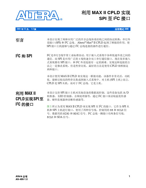
I2C在CPLD上的模拟实现
I2C在CPLD上的模拟实现I2C总线是Philips推出的芯片间串行传输总线,因为其具有需要连线少(仅需一条串行时钟线和一条串行数据线),允许多主机控制,具有裁决和同步功能,可随意添加或摘除总线上的子器件等诸多优点,所以已经被广泛应用。
另外由于Philips和其它厂商提供了种类众多的I2C兼容芯片,促使其成为世界性的工业标准。
对于那些没有硬件I2C接口的MCU,现行大都采用以下两种方法来实现:一种是在程序内部使用模拟I2C的软件包,该方法简单、需要硬件少,但程序开销大,相应速度有所下降,在有些场合不太合适。
另一种是在MCU和I2C器件间加一片CPLD芯片,用该芯片完成模拟I2C的功能。
这种方法虽然增加了硬件开销,但减少了MCU的负担,控制方式要灵活得多。
当然,应用的环境、要求不同,选择的方法也会不同,下面仅就后者进行介绍。
1.I2C规则介绍(1)空闲时SCL和SDA必须保证为高电平,以等待起始位的发生。
(2)启动和停止条件。
在SCL稳定为高电平期间,SDA产生一个由高电平到低电平的跳变,此时即可启动总线,而结束条件与此相反。
(3)位传送。
位传送发生在SCL稳定为高电平期间,此时不允许SDA线上发生数据跳变,否则会导致总线失控。
每个时钟脉冲传送一个数据位。
(4)应答位。
在启动条件和停止条件之间传送器传送给接收器的数据个数没有限制,每个8位字节后加一个应答位。
主传送器产生高电平的应答位,由接收器将该位拉低,称为应答信号(ACK);主器件为接收器时,在接收了最后一个字节后不发应答信号,称为非应答信号(NO ACK)。
从接收器必须在接收到每个字节后产生一个应答位,主接收器也必须在接收从传送器传送的每个字节后产生一个应答位。
(5)写模式。
主传送器首先向数据线发送从接收器地址,地址末尾一位为0,表示要进行写操作,得到应答后便向从接收器发送数据,每发送一个字节,读取一次应答位,为ACK则接着发送,为NO ACK则发送停止位。
利用MAX II CPLD 实现SPI 至I2C 接口
AN-486-1.0
应用笔记 486:利用 MAX II CPLD 实现 SPI 至 I2C 接口
I2C
I2C 主机 SPI 从机 SPI 主机
图 1. 利用 MAX II CPLD 实现 SPI 至 I2C 的接口
Altera MAX II
UP ASIC MCU FPGA
SCLK SS
MOSI MISO
f
请访问下面的网址,下载 SPI 仿真软件:
/files/soft_dev_tools/software/device_driv ers/SPIGen.html
2. 完成注册后,下载并安装 SPIGen。您需要对它进行配置,以适应您 的应用程序以及由 MDN-B2 演示板提供的并口至 SPI 软件狗。
图 4 所示为演示布局。
图 4. 演示布局
基于PC并口的SPI主机 采用了Freescale的 SPIGen
并口至 SPI 接口
CPLD 桥接
DS2745 电池量表
I2C 主机 SPI 从机
Altera 公司
4. 选择16位格式,以十六进制(Intel格式)文件格式(.hex)来显示SPI值。 5. 按照以下步骤来配置 SPI Pins 标签:
f
14. 每次发送 SPI 数据时,使用表 5 的 .hex 数据,单击 Send Once。确定收 到了应答数据。
15. 观察接收到的电池量表数据。收到的有两部分,首先是 MSB 8 位数 据,然后是 LSB 3 位数据 ( 最后一行 )。
16. 改变电池量表模块的黄色预置部分,观察接收数据的变化。黄色预置 部分改变了电池量表芯片 (Maxim DS2745) 的输入电压值,该芯片通 过其 I2C 接口,以 11 位 2 进制兼容格式来提供电压读数。
利用MAX II CPLD,通过SMBus 实现GPIO 引脚扩展
应用笔记484利用MAX II CPLD ,通过SMBus 实现GPIO 引脚扩展引言本应用笔记介绍Altera ® MAX ®II CPLD 通过工业标准系统管理总线(SMBus)来提供通用I/O 引脚扩展功能。
通过SMBus 实现GPIO 引脚扩展为了缩小封装尺寸,减少引脚数量,很多微处理器系统限制了通用I/O (GPIO)引脚的数量, 但是如果系统有SMBus 接口,那么本设计可以通过SMBus 来提供更多的GPIO 引脚。
而且,使用MAX II CPLD 时,这些增加的GPIO 引脚要比微处理器的I/O 引脚功耗低。
在某些情况下,您可能需要远程访问嵌入式系统中的GPIO 引脚。
由于SMBus 接口是2线系统,本设计在远端提供多个输入和输出引脚,不需要其他的连线。
这提高了设计灵活性,降低了复杂度,减少了软件开销。
您可以通过这些通用输出引脚来连接并控制外设控制器、LED 和其他状态指示器。
同样的,您还可以在前面板上连接用户控制、按键以及开关和CPLD 提供的通用输入。
基于MAX IICPLD 的SMBus实现GPIO 引脚扩展MAX II CPLD 用作SMBus 从机,在其SMBus 接口上有两个引脚 :SMBus 时钟SMBCLK 和数据线SMBDAT 。
作为SMBus 主机的主系统和MAX II(用作SMBus 从机)进行通信。
CPLD 为主机提供8个通用输入端口和8个通用输出端口。
GPIO 引脚并行接收由SMBus 串行发送的数据。
这样,可以同时读写所有8个通用I/O(参见图1)。
2007年12月,1.0版图 1.通过SMBus进行GPIO 引脚扩展SMBus接口对于SMBus接口,CPLD提供一个符合常用SMBus协议的内置7位地址。
主机发送起始信号,然后是7位地址和一个读写位。
当总线上广播的地址和从机设备的地址匹配时,根据主机发送的读或者写信号,设备发送一个ACK (应答)信号,然后是DATA。
运用CPLD实现I2C数据写入保护及读取确认的方法[发明专利]
![运用CPLD实现I2C数据写入保护及读取确认的方法[发明专利]](https://img.taocdn.com/s3/m/16961231195f312b3069a577.png)
专利名称:运用CPLD实现I2C数据写入保护及读取确认的方法专利类型:发明专利
发明人:林正中
申请号:CN201810963158.7
申请日:20180822
公开号:CN109271099A
公开日:
20190125
专利内容由知识产权出版社提供
摘要:本发明公开了运用CPLD实现I2C数据写入保护及读取确认的方法,写入方法包括在I2C数据写入的标准封装包中写入INVERT_DATA_BYTE;通过CPLD确认INVERT_DATA_BYTE是否为DATA_BYTE的位元反向值;如果是主控端将数据写入CPLD;否则主控端不将数据写入CPLD。
还涉及读取方法,包括在I2C数据读取的标准封装包中写入INVERT_DATA_BYTE;主控端从CPLD读取INVERT_DATA_BYTE及DATA_BYTE,并判断INVERT_DATA_BYTE的值是否为DATA_BYTE的位元反向值;如果是主控端成功读取数据;否则重新读取数据。
本发明通过在标准封装包中增加INVERT_DATA_BYTE,降低了数据读取错误及被恶意篡改的风险,有效加强了数据的安全保护。
申请人:郑州云海信息技术有限公司
地址:450018 河南省郑州市郑东新区心怡路278号16层1601室
国籍:CN
代理机构:济南诚智商标专利事务所有限公司
代理人:黄蓉
更多信息请下载全文后查看。
应用CPLD实现ASI_SPI接口转换的方法
应用CP LD 实现ASI -SPI 接口转换的方法□廖晓维,朱 红(电子科技大学,四川成都610054)摘 要:遵照国家的DVB 标准及SPI 接口标准,提出一种不需要使用FIFO ,就能恢复出SPI 接口的PSY NC 、DAV LI D 信号的方案。
经硬件实现,仅使用CP LD 芯片就能完成该功能,实时稳定地产生出PSY NC 、DAV LI D 信号,避免了使用FPG A 芯片及FIFO 带来的高成本问题。
对SPI 时钟的恢复提出一种新的解决方法,简化了ASI —SPI 转换卡的硬件设计。
关键词:CP LD ;ASI ;SPI ;接口转换中图分类号:T N911.25 文献标识码:A 文章编号:1007-7022(2004)18-0074-02Converting Signals from ASI to SPI Using CP LD□LI AO X iao 2wei ,ZH U H ong(University of Electronic and T echnology ,Sichuan Chengdu 610054,China )Abstract :We gave a new alg orithm to convert signals from ASI to SPI without FIFO ,according to the national DVB standard and SPI interface standard.This method can recover PSY NC and DAV LI D signals only use CP LD chips ,reduced the cost.And m ore in this paper we found a new way to recover SPI clock ,which sim plified the hardware design of ASI -SPI card.K ey w ords :CP LD ;ASI ;SPI ;Interface C onversion1 引言在数字技术高速发展的今天,可编程逻辑器件的制造工艺不断提高,CP LD 等可编程器件的速度和规模也有了很大的提高,而且具有集成度高、体积小、功耗低、设计灵活等优点。
- 1、下载文档前请自行甄别文档内容的完整性,平台不提供额外的编辑、内容补充、找答案等附加服务。
- 2、"仅部分预览"的文档,不可在线预览部分如存在完整性等问题,可反馈申请退款(可完整预览的文档不适用该条件!)。
- 3、如文档侵犯您的权益,请联系客服反馈,我们会尽快为您处理(人工客服工作时间:9:00-18:30)。
利用 MAX II CPLD 实现 SPI 至 I2C 的接口
本设计支持 SPI 接口主机对其他设备的数据流控制,这些设备包括 A/D 转换器、 LED 控制器、音频处理器等,通过 I2C 接口来读取温度传感 器、硬件监视器和诊断传感器等。
f
14. 每次发送 SPI 数据时,使用表 5 的 .hex 数据,单击 Send Once。确定收 到了应答数据。
15. 观察接收到的电池量表数据。收到的有两部分,首先是 MSB 8 位数 据,然后是 LSB 3 位数据 ( 最后一行 )。
16. 改变电池量表模块的黄色预置部分,观察接收数据的变化。黄色预置 部分改变了电池量表芯片 (Maxim DS2745) 的输入电压值,该芯片通 过其 I2C 接口,以 11 位 2 进制兼容格式来提供电压读数。
利用 MAX II CPLD 实现 SPI 至 I2C 接口
2007 年 12 月, 1.0 版
应用笔记 486
引言
本设计实现了两种应用广泛的共享总线体系结构之间的协议转换:串行外 设接口 (SPI) 和 I2C 总线。 Altera® Max® II CPLD 起到了桥接的作用,使 SPI 接口主机能够与通过 I2C 总线连接的器件进行通信。
01 00 (ack) 80 91 ( 启动 + 从机地址 )
01 00 (ack) 20 00 ( 读 ) 01 ?? (ack + MSB 数据 ) 00 00 ( 没有操作 ) 01 ?? (ack + LSB 数据 )
Altera 公司
7
应用笔记 486:利用 MAX II CPLD 实现 SPI 至 I2C 接口
寄存器中的数据
从机地址 + R/W 要写入的数据 不重要 不重要 不重要
某一 I2C 操作读入的数据存储在数据输出寄存器中,由 SPI 主机在下一 SPI 操作中读取。 SPI 主机需要最后一个命令字 00000000 (b) 来读取状态 值,而数据输出寄存器对 I2C 总线不作任何操作。 I2C 命令格式如图 3 所 示。
信号 I2C_scl: I2C_sda SPI_cs SPI_miso SPI_mosi SPI_clk
引脚分配
引脚
引脚 39 引脚 40 引脚 95 引脚 91 引脚 92 引脚 96
1 在 Quartus® II 软件的器件和引脚选项设置中,将未使用的引脚 分配为 input tri-stated。在引脚分配过程中,在 Quartus II 软 件的 I/O 标准栏中,将 SPI_sclk 分配为 2.5-V 施密特触发器 输入。Quartus II 软件的分配编辑器被用于使能 I2C_scl 和 I2C_sda 引脚的 Auto Open Drain。打开相应的设置后,对设 计进行编译。
信号 SS SCLK MISO MOSI
目的
从机选择 SPI 时钟 主机输入从机输出 主机输出从机输入
方向
输入 ( 低电平有效 ) 输入 输出 输出
SPI 主机发送:
■ 命令寄存器 (8 位 ) ■ 数据输入 (8 位 )
SPI 主机接收:
■ 状态寄存器 (8 位 ) ■ 数据输出 (8 位 )
SPI 字长度固定为 16 比特。如图 2 所示,CPOL = 0 和 CPHA = 1。在每一 个 SPI 字中,命令寄存器规定 I2C 总线上的功能,数据输入保持 I2C 总线 要发送的数据。类似的,状态寄存器的最后一位是应答位,数据输出是在 前一 I2C 周期中通过 I2C 线接收到的数据。
a. 保持引脚分配的默认设置不变 (Chip Select: 2, Data In: 3, Data Out: 12, Clock: 4)。
b. 保持 Bit Order 的默认设置 MSB is sent first 不变。 c. 将 Chip Select 改为 High when asserted。 d. 将 Data In 和 Data out 改为 Low = 1。 e. 将 SPI Type 改为 Type 4。
图 1 所示为采用 MAX II CPLD 来实现 SPI 至 I2C 的接口。它作为 SPI 从 机和 SPI 主机进行接口,使用了四种信号线,控制用的 SS 和 SCLK 信 号,数据用的 MISO 和 MOSI 信号。I2C 总线一侧接口有两条信号线, SCLK 和 SDA 信号。
Altera 公司
图 3. I2C 命令格式
Start Slave addresA/A' Stop
主机写操作
从机写操作
Altera 公司
4
应用笔记 486:利用 MAX II CPLD 实现 SPI 至 I2C 接口
设计实现
本设计可以采用 EPM240 或者其他 MAX II CPLD 来实现。实现过程涉及 到使用设计源代码,为 MAX II CPLD 的通用 I/O (GPIO) 线分配相应的 信号和控制线等。在演示设计实现时,还需要一个 SPI 主机和一个 I2C 从 机。
如果需要了解详细信息,请参考:
/quick_view2.cfm/qv_pk/4994
在每一 SPI 总线的最后,从机选择线变为高电平,指示完成一个字的发 送,对于此时命令寄存器中的每个值,执行一个 I2C 总线周期。经过固定 时延后,根据 I2C SCL 上的频率,可以发送另一个 SPI 字。两个 SPI 字之 间的最小时延是 I2C SCL 时钟频率。
Altera 公司
3
应用笔记 486:利用 MAX II CPLD 实现 SPI 至 I2C 接口
I2C 和 SPI
I2C 是串行 2 线窄带工业标准协议,用于嵌入式系统中各种低速外设之间的 通信。而 SPI 是应用广泛的 4 线快速全双工串行通信接口。现在很多嵌入 式系统都有 SPI 接口,和 I2C 外设连接有一定的困难。实现这种连接的方 法之一是修改系统,但是性价比低。最好的方法是使用 CPLD 来桥接这 两种接口。
1
AN-486-1.0
应用笔记 486:利用 MAX II CPLD 实现 SPI 至 I2C 接口
I2C
I2C 主机 SPI 从机 SPI 主机
图 1. 利用 MAX II CPLD 实现 SPI 至 I2C 的接口
Altera MAX II
UP ASIC MCU FPGA
SCLK SS
MOSI MISO
根据从 SPI 一侧接收到的命令寄存器值来执行 I2C 功能。表 3 列出了命令 寄存器中存储的重要命令。
表 3. I2C 命令
命令寄存器
10000000 01000000 00100000 00010000 00000000
I2C 线的目的
启动 / 重新启动 写入一个字节 读取一个字节
停止 空,等待状态
CPLD 桥接
A/D D/A 转换器
SCLK SDA
LCD/LED INT
温度 传感器
EEPROM
MCU
SPI 接口
SPI 总线通常只有一个主机以及和它相连的多个从机。 CPLD 作为从机之 一和 SPI 主机设备相连,实现桥接功能。图 2 所示为 SPI 时序图。表 1 对 SPI 接口引脚进行了说明。
f
请访问下面的网址,下载 SPI 仿真软件:
/files/soft_dev_tools/software/device_driv ers/SPIGen.html
2. 完成注册后,下载并安装 SPIGen。您需要对它进行配置,以适应您 的应用程序以及由 MDN-B2 演示板提供的并口至 SPI 软件狗。
设计说明
请按照以下步骤,在 MDN-B2 演示板上对设计进行演示:
1. 使用 PC 及其并口,下载 SPI 仿真软件以建立 SPI 环境,例如来自 Freescale 的 SPIGen。接受了 Freescale 的使用条款,并免费注册后, 可免费下载该软件。
Altera 公司
5
应用笔记 486:利用 MAX II CPLD 实现 SPI 至 I2C 接口
3. 打开 SPIGen 软件,单击 Configure 菜单。选择 Edit Configuration。 在 General 标签中,确定默认的 Port Address 是正确的 PC 并口地 址。如果不是,进行正确的选择。您可以查看下面的设置,找到 PC 的并口地址:Control Panel > System > Hardware > Device Manager > Ports > ECP Printer Port (LPT1) > Resources。
以下步骤详细说明了这一设计演示,演示用到了 MDN-B2 电路板,以及 采用了 Freescale SPIGen 软件 ( 以及对应的并口硬件 ) 的 PC 并口 SPI 环 境和 I2C 从机电池量表模块 ( 由 MDN-B2 提供 )。
表 4 列出了 EPM240G 的引脚分配。
表 4. EPM240G 引脚分配
图 2. SPI 时序图
SCLK CPOL=0
CPOL=1 SS
CPHA=0
CYCLE #
0
1
MOSI Z 0
1
MISO Z 0
1
2
3
2
3
2
3
4
5
4
5
4
5
6
7
6
7
Z
6
7
Z
Altera 公司
2