FHBAS40-05(SOT-23)肖特基二极管规格书
FHBAS70(SOT-23)肖特基二极管规格书

ቆᄂऔSchottky DiodeSchottky Diode ቆᄂऔFHBAS701DESCRIPTION & FEATURES 概述及特點 SOT-23Low forward voltage 低正向壓降High breakdown voltage 高反向擊穿電壓 Ultra high-speed switching 超高速開關應用 Protection circuits 保護電路應用PIN ASSIGNMENT 引腳說明 PIN NUMBER 引腳序號PIN NAME 管腳符號 SOT-23 FUNCTION 功能 A 1 AnodeNC 2 - C 3 CathodeMAXIMUM RATINGS(T a =25℃) 最大額定值CHARACTERISTIC 特性參數 Symbol 符號Rating 額定值 Unit 單位 Reverse Voltage 反向電壓 V R 70 Vdc Peak Forward Current 正向峰值電流 I F 70 mAdcPeak Forward Surge Current 正向最大浪湧電流t ≤1s I FM(surge) 100 mAdcTHERMAL CHARACTERISTICS 熱特性CHARACTERISTIC 特性參數 Symbol 符號Max 最大值 Unit 單位Total Device Dissipation FR-5 Board(1) T A =25℃ P D 225 mW Total Device Dissipation Alumina Substrate,(2) T A =25℃總耗散功率 氧化鋁襯底P D 300 mWJunction and Storage Temperature 結溫和儲存溫度T J ,T stg 150, -55 ~150℃ 1. FR-5=1.0×0.75×0.062in,printed-circuit board. 2. Alumina=0.4×0.3×0.024in,99.5%aluminaDEVICE MARKING 打標 FHBAS70=K1ELECTRICAL CHARACTERISTICS 電特性(T A =25℃ unless otherwise noted 如無特殊說明,溫度為25℃)Characteristic 特性參數Symbol 符號 Test Condition測試條件Min 最小值Type 典型值 Max 最大值Unit 單位Reverse Voltage Leakage Current反向漏電流I R V R =50Vdc— — 0.1 µA Reverse Breakdown Voltage反向擊穿電壓V (BR)I BR =10μAdc 70 — — Vdc I F =1mAdc— — 410 I F =10mAdc— — 750 Forward Voltage 正向電壓 V F I F =15mAdc— — 1000 mV Total Capacitance 電容 C TV R =0V,f=1.0MHz ——2.0pF。
肖特基二极管常用参数大全
肖特基二极管常用参数大全肖特基二极管常用参数大全肖特基二极管常用参数大全型号制造商封装If/A Vrrm/V最大Vf/V1SS294 TOS SC-59 0.1 400.60BAT15-099 INF SOT143 0.11 4 0.32BAT54A PS SOT23 0.20 300.5010MQ060N IR SMA 0.77 900.6510MQ100N IR SMA 0.77 1000.9610BQ015 IR SMB 1.00 150.34SS12 GS DO214 1.00 20 0.50MBRS130LT3 ON - 1.00 300.3910BQ040 IR SMB 1.00 400.53RB060L-40 ROHM PMDS 1.00 400.55RB160L-40 ROHM PMDS 1.00 400.55SS14 GS DO214 1.00 40 0.50MBRS140T3 ON - 1.00 400.6010BQ060 IR SMB 1.00 600.57SS16 GS DO214 1.00 60 0.7510BQ100 IR SMB 1.00 100 0.78MBRS1100T3 ON - 1.00 100 0.7510MQ040N IR SMA 1.10 40 0.5115MQ040N IR SMA 1.70 40 0.55PBYR245CT PS SOT223 2.00 45 0.4530BQ015 IR SMC 3.00 15 0.3530BQ040 IR SMC 3.00 40 0.5130BQ060 IR SMC 3.00 60 0.5830BQ100 IR SMC 3.00 100 0.79STPS340U STM SOD6 3.00 400.84MBRS340T3 ON - 3.00 40 0.52RB051L-40 ROHM PMDS 3.00 40 0.45MBRS360T3 ON - 3.00 60 0.7030WQ04FN IR DPAK 3.30 40 0.6230WQ06FN IR DPAK 3.30 60 0.7030WQ10FN IR DPAK 3.30 100 0.9130WQ03FN IR DPAK 3.50 30 0.5250WQ03FN IR DPAK 5.50 30 0.5350WQ06FN IR DPAK 5.50 60 0.576CWQ06FN IR DPAK 6.60 600.586CWQ10FN IR DPAK pr 6.60 1000.811N5817 ON 轴向 1.00 20 0.75 1N5818 ON 轴向 1.00 30 0.55SB130 GS 轴向 1.00 30 0.50 1N5819 ON 轴向 1.00 40 0.60 MBR150 ON 轴向 1.00 501.00MBR160 ON 轴向 1.00 601.0011DQ10 IR 轴向 1.10 100 0.8511DQ04 IR 轴向 1.10 40 0.55 11DQ05 IR 轴向 1.10 50 0.58 11DQ06 IR 轴向 1.10 60 0.58MBRS340TR IR SMC 3.00 400.431N5820 ON 轴向 3.00 20 0.85 1N5821 ON 轴向 3.00 30 0.38 1N5822 ON 轴向 3.00 40 0.52MBR360 ON 轴向 3.00 601.00SS32 GS DO214 3.00 20 3.00 SS34 GS DO214 3.00 40 0.50 31DQ10 IR DO201 3.30 100 0.85SB530 GS 轴向 5.00 30 0.57 SB540 GS DO201 5.00 40 0.57 50SQ080 IR 轴向 5.00 80 0.66 50SQ100 IR 轴向 5.00 100 0.66 MBR735 GS TO220 7.50 350.84MBR745 GS TO220 7.50 450.84MBR745 IR TO220 7.50 450.8480SQ040 IR 轴向8.00 40 0.53 STQ080 IR TO220 8.00 80 0.72 8TQ100 TO220 8.00 100 0.72 80SQ040 IR 轴向8.00 40 0.5380SQ035 IR DO204AR 8.00 350.53HFA16PA60C IR TO247CT 8.00 6001.7095SQ015 轴向9.00 15 0.3190SQ040 轴向9.00 40 0.48 10TQ045 TO220 10.00 45 0.57 MBR1035 GS TO220 10.00 350.84MBR1045 ON TO220 10.00 450.84STPS1045F ON ISO220 10.00 45 0.64MBR2060CT ON TO220 10.00 600.85 <P style="TEXT-INDE。
DIODES贴片肖特基二极管BAS40选型手册

SURFACE MOUNT SCHOTTKY BARRIER DIODEProduct Summary @T A = +25°CV RRM (V) I O (mA) V Fmax (V)I Rmax (μA)40 200 1.0 0.2Description200mA surface mount Schottky Barrier Diode in SOT23 package, offers low forward voltage drop and fast switching capability, designed with PN Junction Guard Ring for Transient and ESD Protection, totally lead-free finish and RoHS compliant, ”Green” device.Features and Benefits∙Low Forward Voltage Drop∙ Fast Switching ∙ PN Junction Guard Ring for Transient and ESD Protection∙ Lead-Free Finish; RoHS Compliant (Notes 1 & 2) ∙ Halogen and Antimony Free. “Green” Device (Note 3) ∙Qualified to AEC-Q101 Standards for High ReliabilityMechanical Data∙ Case: SOT23 ∙ Case Material: Molded Plastic. UL Flammability Classification Rating 94V-0∙ Moisture Sensitivity: Level 1 per J-STD-020D∙ Terminals: Solderable per MIL-STD-202, Method 208 ∙ Lead Free Plating (Matte Tin Finish annealed over Alloy 42 leadframe).∙ Polarity: See Diagrams Below ∙ Weight: 0.008 grams (approximate)Top View BAS40 BAS40-04 BAS40-05BAS40-06Ordering Information (Note 4 & 5)Part NumberCase Packaging BAS40-7-F / BAS40Q-7-F SOT23 3000/Tape & Reel BAS40-04-7-F / BAS40-04Q-7-F SOT23 3000/Tape & Reel BAS40-05-7-F / BAS40-05Q-7-F SOT23 3000/Tape & Reel BAS40-06-7-F / BAS40-06Q-7-F SOT23 3000/Tape & Reel BAS40-13-F / BAS40Q-13-F SOT23 10000/Tape & Reel BAS40-04-13-F / BAS40-04Q-13-F SOT23 10000/Tape & Reel BAS40-05-13-F / BAS40-05Q-13-F SOT23 10000/Tape & Reel BAS40-06-13-F / BAS40-06Q-13-FSOT23 10000/Tape & ReelNotes: 1. No purposely added lead. Fully EU Directive 2002/95/EC (RoHS) & 2011/65/EU (RoHS 2) compliant.2. See /quality/lead_free.html for more information about Diodes Incorporated’s definitions of Halogen- and Antimony-free, "Green" and Lead-free.3. Halogen- and Antimony-free "Green” products are defined as those which contain <900ppm bromine, <900ppm chlorine (<1500ppm total Br + Cl) and <1000ppm antimony compounds.4. For packaging details, go to our website at /products/packages.html.5. Products manufactured with Date Code V9 (week 33, 2008) and newer are built with Green Molding Compound. Products manufactured prior to Date Code V9 are built with Non-Green Molding Compound and may contain Halogens or Sb 2O 3 Fire Retardants.e3Marking InformationDate Code Key Year 1999 2000 2001 2002 2003 20042005 2006 2007 2008 2009 2010 2011 2012 2013 2014 2015 Code K L MN P R S T U V W X Y Z A B CMonth Jan Feb Mar Apr May Jun Jul Aug Sep Oct Nov Dec Code 1 2 3 4 5 6 7 8 9 O N DMaximum Ratings (@T A = +25°C, unless otherwise specified.)CharacteristicSymbol Value Unit Peak Repetitive Reverse Voltage Working Peak Reverse Voltage DC Blocking VoltageV RRM V RWM V R 40 V Forward Continuous Current (Note 6) I FM 200 mA Forward Surge Current (Note 6) @ t < 1.0sI FSM600mAThermal CharacteristicsCharacteristicSymbol Value Unit Power Dissipation (Note 6)P D 350 mW Thermal Resistance, Junction to Ambient Air (Note 6) R θJA 357 °C/W Operating Temperature Range T J -55 to +125 °C Storage Temperature Range T STG-65 to +150°CElectrical Characteristics (@T A = +25°C, unless otherwise specified.)CharacteristicSymbol Min Typ Max Unit Test ConditionReverse Breakdown Voltage (Note 7) V (BR)R 40 − − V I R = 10µAForward VoltageV F − − 380 1000 mV t p < 300µs, I F = 1.0mA t p < 300µs, I F = 40mA Reverse Leakage Current (Note 7) I R − 20 200 nA t p < 300µs, V R = 30V Total Capacitance C T − 4.0 5.0 pF V R = 0V, f =1.0MHzReverse Recovery Timet rr−−5.0nsI F = I R = 10mA to I R = 1.0mA, R L = 100ΩNotes: 6. Part mounted on FR-4 board with recommended pad layout, which can be found on our website at /datasheets/ap02001.pdf. 7. Short duration pulse test used to minimize self-heating effect.xxx = Product Type Marking CodeK43 = BAS40 K44 = BAS40-04 K45 = BAS40-05 K46 = BAS40-06YM = Date Code Marking for SAT (Shanghai Assembly/ Test site) Y M = Date Code Marking for CAT (Chengdu Assembly/ Test site) Y or Y = Year (ex: A = 2013) M = Month (ex: 9 = September)Chengdu A/T SiteShanghai A/T SiteT , AMBIENT TEMPERATURE (ºC)Figure 1 Power Derating Curve, T otal Package A P , P O W E R D I S S I P A T I O N (m W )D 01002003004000.010.110.0001I , I N S T A N T A N E O U S F O R W A R D C U R R E N T (A )F V , INSTANTANEOUS FORWARD VOLTAGE (V)Figure 2 Typical Forward CharacteristicsF 1101001,00010,000V , INSTANTANEOUS REVERSE VOLTAGE (V)Figure 3 Typical Reverse Characteristics R I , I N S T A N T A N E O U S R E V E R S E C U R R E N T (n A )R 220C , T O T A L C A P A C I T A N C E (p F )T V , DC REVERSE VOLTAGE (V)Figure 4 Total Capacitance vs. Reverse VoltageRPackage Outline DimensionsPlease see AP02002 at /datasheets/ap02002.pdf for latest version.Suggested Pad LayoutPlease see AP02001 at /datasheets/ap02001.pdf for the latest version.SOT23Dim Min Max Typ A 0.37 0.51 0.40 B 1.20 1.40 1.30 C 2.30 2.50 2.40 D 0.89 1.03 0.915F 0.45 0.60 0.535G 1.78 2.05 1.83 H 2.80 3.00 2.90 J 0.013 0.10 0.05 K 0.890 1.00 0.975K1 0.903 1.10 1.025L 0.45 0.61 0.55 L1 0.25 0.55 0.40 M 0.085 0.150 0.110a 8°All Dimensions in mmDimensions Value (in mm)Z 2.9 X 0.8 Y 0.9 C 2.0 E1.35X EYCZA l l 7°IMPORTANT NOTICEDIODES INCORPORATED MAKES NO WARRANTY OF ANY KIND, EXPRESS OR IMPLIED, WITH REGARDS TO THIS DOCUMENT, INCLUDING, BUT NOT LIMITED TO, THE IMPLIED WARRANTIES OF MERCHANTABILITY AND FITNESS FOR A PARTICULAR PURPOSE (AND THEIR EQUIVALENTS UNDER THE LAWS OF ANY JURISDICTION).Diodes Incorporated and its subsidiaries reserve the right to make modifications, enhancements, improvements, corrections or other changes without further notice to this document and any product described herein. Diodes Incorporated does not assume any liability arising out of the application or use of this document or any product described herein; neither does Diodes Incorporated convey any license under its patent or trademark rights, nor the rights of others. Any Customer or user of this document or products described herein in such applications shall assume all risks of such use and will agree to hold Diodes Incorporated and all the companies whose products are represented on Diodes Incorporated website, harmless against all damages.Diodes Incorporated does not warrant or accept any liability whatsoever in respect of any products purchased through unauthorized sales channel. Should Customers purchase or use Diodes Incorporated products for any unintended or unauthorized application, Customers shall indemnify and hold Diodes Incorporated and its representatives harmless against all claims, damages, expenses, and attorney fees arising out of, directly or indirectly, any claim of personal injury or death associated with such unintended or unauthorized application.Products described herein may be covered by one or more United States, international or foreign patents pending. Product names and markings noted herein may also be covered by one or more United States, international or foreign trademarks.This document is written in English but may be translated into multiple languages for reference. Only the English version of this document is the final and determinative format released by Diodes Incorporated.LIFE SUPPORTDiodes Incorporated products are specifically not authorized for use as critical components in life support devices or systems without the express written approval of the Chief Executive Officer of Diodes Incorporated. As used herein:A. Life support devices or systems are devices or systems which:1. are intended to implant into the body, or2. support or sustain life and whose failure to perform when properly used in accordance with instructions for use provided in thelabeling can be reasonably expected to result in significant injury to the user.B. A critical component is any component in a life support device or system whose failure to perform can be reasonably expected to cause thefailure of the life support device or to affect its safety or effectiveness.Customers represent that they have all necessary expertise in the safety and regulatory ramifications of their life support devices or systems, and acknowledge and agree that they are solely responsible for all legal, regulatory and safety-related requirements concerning their products and any use of Diodes Incorporated products in such safety-critical, life support devices or systems, notwithstanding any devices- or systems-related information or support that may be provided by Diodes Incorporated. Further, Customers must fully indemnify Diodes Incorporated and its representatives against any damages arising out of the use of Diodes Incorporated products in such safety-critical, life support devices or systems. Copyright © 2013, Diodes Incorporated。
BAS40-05中文资料
.30 (7.5) .12 (3)
.04 (1)
.08 (2) .04 (1) .08 (2)
.59 (15) .47 (12)
.03 (0.8)
0.2 (5)
.06 (1.5) .20 (5.1)
Dimensions in inches (millimeters)
Layout for RthJA test Thickness: Fiberglass 0.059 in (1.5 mm) Copper leads 0.012 in (0.3 mm)
1)
Value 40 2001) 6001) 2001) 150 –55 to +150
Unit V mA mA mW °C °C
VRRM IF IFSM Ptot Tj TS
Device on fiberglass substrate, see layout
4/98
元器件交易网
元器件交易网
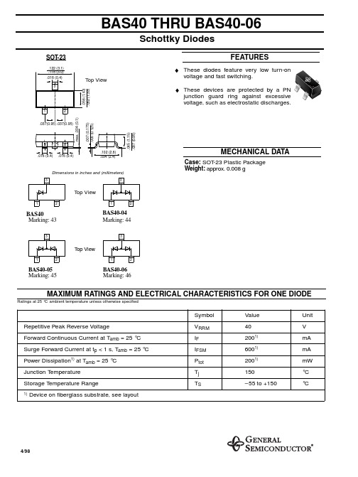
BAS40 THRU BAS40-06
Schottky Diodes
SOT-23
.122 (3.1) .118 (3.0) .016 (0.4) 3
FEATURES ♦ These diodes feature very low turn-on
Top View
BAS40 THRU BAS40-06
ELECTRICAL CHARACTERISTICS
Ratings for one diode at 25 °C ambient temperature unless otherwise specified
Symbol Reverse Breakdown Voltage Tested with 10 µA Pulses Leakage Current Pulse Test tp < 300 µs at VR = 30 V Forward Voltage Pulse Test tp < 300 µs at IF = 1 mA at IF = 40 mA Capacitance at VR = 0 V, f = 1 MHz Reverse Recovery Time from IF = 10 mA through IR = 10 mA to IR = 1 mA Thermal Resistance Junction to Ambient Air
BAS40-05 丝印45 开关二极管选型手册

0
0.25 0.20 0.15 0.10 0.05 0.00
0
Reverse Characteristics
T =100℃ a
T =25℃ a
10
20
30
40
REVERSE VOLTAGE V (V) R
Power Derating Curve
25
50
75
100
125
AMBIENT TEMPERATURE T (℃) a
【领先的片式无源器件整合供应商—南京南山半导体有限公司】
JIANGSU CHANGJIANG ELECTRONICS TECHNOLOGY CO., LTD
SOT-23 Plastic-Encapsulate Diodes
BAS40/-04/-05/-06 SCHOTTKY BARRIER DIODE
FEATURES z Low Forward Voltage z Fast Switching
SOT-23
BAS40 MARKING: 43•
BAS40-06 MARKING: 46
Maximum Ratings @Ta=25℃
BAS40-05 MARKING:45 BAS40-04 MARKING:44
回访记录
□已联系确认 日期:
□已建议执行 日期:
□未发送但已下单 日期:
□已发送样品 日期:
□客户已签收 日期:
第1页共1页
Symbol
VRRM VRWM
VR IFM PD RθJA TJ TSTG
Limit
40
200 200 500 125 -55~+150
Unit
FOSAN富信电子 二级管 BAS40-产品规格书

安徽富信半导体科技有限公司ANHUI FOSAN SEMICONDUCTOR TECHNOLOGY CO.,LTD.BAS40/-04/-05/-06SOT-23Schottky Barrier Diode 肖特基势垒二极管▉Internal Configuration&DeviceMarking 内部结构与产品打标Type 型号BAS40BAS40-04BAS40-05BAS40-06Pin 管脚Mark 打标43444546▉AbsoluteMaximum Ratings 最大额定值Characteristic 特性参数Symbol 符号Rat 额定值Unit 单位Peak Reverse V oltage 反向峰值电压V RRM 40V Reverse Work Voltage 反向工作电压V RWMDC Reverse Voltage 直流反向电压V R Forward Work Current 正向工作电流I F (I O )200mA Peak Forward Current 正向峰值电流I FM600mA Power dissipation 耗散功率P D (Ta=25℃)200mW Thermal Resistance J-A 结到环境热阻R θJA 625℃/WJunction and Storage Temperature 结温和储藏温度T J ,T stg-55to+150℃■Electrical Characteristics 电特性(T A =25℃unless otherwise noted 如无特殊说明,温度为25℃)Characteristic 特性参数Symbol 符号Min 最小值Max 最大值Unit 单位Reverse Breakdown Voltage 反向击穿电压(I R =10µA)V (BR)40—V Reverse Leakage Current 反向漏电流(V R =30V)I R —200nA Forward V oltage(I F =1mA)正向电压(I F =40mA)V F —0.381V Diode Capacitance 二极管电容(V R =0V,f=1MHz)C T—5pF Reverse Recovery Time 反向恢复时间T rr—5nSANHUI FOSAN SEMICONDUCTOR TECHNOLOGY CO.,LTD.BAS40/-04/-05/-06■Typical Characteristic Curve典型特性曲线ANHUI FOSAN SEMICONDUCTOR TECHNOLOGY CO.,LTD.BAS40/-04/-05/-06■Dimension外形封装尺寸Symbol Dimensions In Millimeters Dimensions In Inches Min Max Min Max A 0.900 1.1500.0350.045A10.0000.1000.0000.004A20.900 1.0500.0350.041b 0.3000.5000.0120.020c 0.0800.1500.0030.006D 2.800 3.0000.1100.118E 1.200 1.4000.0500.055E1 2.2502.5500.0890.100e 0.950TYP0.037TYPe1 1.8002.0000.0710.079L 0.550REF0.022REFL10.3000.5000.0120.020θ0o8o 0o8o。
WSD420 SOT-23 肖特基二极管 使用说明书
Symbol VRM VR IO I FSM Tj TSTG
Limits 40 40 100 1 125
-40 + 125
Unit V V
mA A C C
Electrical Characteristics (TA=25 C Unless Otherwise Note)
Characteristic
Forward Voltage, I F =10mA Reverse Current, VF =10V Capacitance Between Terminals VR =10V
SMALL SIGNAL SCHOTTKY DIODES
100m AMPERES 40 VOLTS
3 1
2
SOT-23
SOT-23 Outline Dimensions
A
TOP VIEW
BC
E
GD
H
K
L J
Unit:mm
Dim Min Max
A 0.35 0.51
B 1.19 1.40
C 2.10 3.00
100n
T a=125ûC 75ûC 25ûC
10n 0
5 10 15 20 25 30 35 REVERSE VOLTAGE : VR (V)
FIG2. Reverse cWEEN TERMINALS : CT (pF)
100 50
20 10
Characteristic Peak Reverse Voltage DC Reverse Voltage Mean Rectifying Current Peak Forward Surge Current (1) Junction Temperature Storage Temperature
KMA2D4P20SA SOT-23规格书
SYMBOL
TEST CONDITION
MIN.
TYP.
MAX.
UNIT
BVDSS IDSS
VGS=0V, ID=-250 A VGS=0V, VDS=-20V VGS=0V, VDS=-16V, Tj=70
-20 -0.6
(Note2) (Note2) (Note2) (Note2)
83 145 4
-1
-1.2
Junction Temperature Tj ( C)
Source to Drain Forward Voltage VSD (V)
2011. 12. 22
Revision No : 3
3/4
KMA2D4P20SA
2011. 12. 22
Revision No : 3
4/4
0 0
-0.5 -1.0 -1.5 -2.0 -2.5 -3.0
Drain to Source Voltage VDS (V)
Drain Current ID (A)
Drain to Source On Resistance RDS(ON) (mΩ)
Fig3. ID - VGS
-10
VDS = VGS
(Note1) (Note1) (Note1) (Note1) (Note1)
VDSS VGSS ID IDP PD
-20 12 -2.4
V V A
SOT-23
-9 1.25 W 0.6 150 -55 150 100 /W
Type Name
Marking
Lot No.
Tj Tstg RthJA
KB2
Fig2. RDS(ON) - ID
肖特基二极管通用参数全套汇编
肖特基二极管常用参数大全肖特基二极管常用参数大全肖特基二极管常用参数大全型号制造商封装If/A Vrrm/V最大Vf/V1SS294 TOS SC-59 0.1 400.60BAT15-099 INF SOT143 0.11 4 0.32BAT54A PS SOT23 0.20 300.5010MQ060N IR SMA 0.77 900.6510MQ100N IR SMA 0.77 1000.9610BQ015 IR SMB 1.00 150.34SS12 GS DO214 1.00 20 0.50MBRS130LT3 ON - 1.00 300.3910BQ040 IR SMB 1.00 400.53RB060L-40 ROHM PMDS 1.00 400.55RB160L-40 ROHM PMDS 1.00 400.55SS14 GS DO214 1.00 40 0.50MBRS140T3 ON - 1.00 400.6010BQ060 IR SMB 1.00 600.57SS16 GS DO214 1.00 60 0.7510BQ100 IR SMB 1.00 100 0.78MBRS1100T3 ON - 1.00 100 0.7510MQ040N IR SMA 1.10 40 0.5115MQ040N IR SMA 1.70 40 0.55PBYR245CT PS SOT223 2.00 45 0.4530BQ015 IR SMC 3.00 15 0.3530BQ040 IR SMC 3.00 40 0.5130BQ060 IR SMC 3.00 60 0.5830BQ100 IR SMC 3.00 100 0.79STPS340U STM SOD6 3.00 400.84MBRS340T3 ON - 3.00 40 0.52RB051L-40 ROHM PMDS 3.00 40 0.45MBRS360T3 ON - 3.00 60 0.7030WQ04FN IR DPAK 3.30 40 0.6230WQ06FN IR DPAK 3.30 60 0.7030WQ10FN IR DPAK 3.30 100 0.9130WQ03FN IR DPAK 3.50 30 0.5250WQ03FN IR DPAK 5.50 30 0.5350WQ06FN IR DPAK 5.50 60 0.576CWQ06FN IR DPAK 6.60 600.586CWQ10FN IR DPAK pr 6.60 1000.811N5817 ON 轴向 1.00 20 0.75 1N5818 ON 轴向 1.00 30 0.55SB130 GS 轴向 1.00 30 0.50 1N5819 ON 轴向 1.00 40 0.60 MBR150 ON 轴向 1.00 501.00MBR160 ON 轴向 1.00 601.0011DQ10 IR 轴向 1.10 100 0.8511DQ04 IR 轴向 1.10 40 0.55 11DQ05 IR 轴向 1.10 50 0.58 11DQ06 IR 轴向 1.10 60 0.58MBRS340TR IR SMC 3.00 400.431N5820 ON 轴向 3.00 20 0.85 1N5821 ON 轴向 3.00 30 0.38 1N5822 ON 轴向 3.00 40 0.52MBR360 ON 轴向 3.00 601.00SS32 GS DO214 3.00 20 3.00 SS34 GS DO214 3.00 40 0.50 31DQ10 IR DO201 3.30 100 0.85SB530 GS 轴向 5.00 30 0.57 SB540 GS DO201 5.00 40 0.57 50SQ080 IR 轴向 5.00 80 0.66 50SQ100 IR 轴向 5.00 100 0.66 MBR735 GS TO220 7.50 350.84MBR745 GS TO220 7.50 450.84MBR745 IR TO220 7.50 450.8480SQ040 IR 轴向8.00 40 0.53 STQ080 IR TO220 8.00 80 0.72 8TQ100 TO220 8.00 100 0.72 80SQ040 IR 轴向8.00 40 0.5380SQ035 IR DO204AR 8.00 350.53HFA16PA60C IR TO247CT 8.00 6001.7095SQ015 轴向9.00 15 0.3190SQ040 轴向9.00 40 0.48 10TQ045 TO220 10.00 45 0.57 MBR1035 GS TO220 10.00 350.84MBR1045 ON TO220 10.00 450.84STPS1045F ON ISO220 10.00 45 0.64MBR2060CT ON TO220 10.00 600.85 <P style="TEXT-INDE。
SMD元件选用指南
46
TOSHIBA变容二极管
1SV214 SOD-323,C2V=14.16~16.25PF C25V=2.11~2.43PF 1SV215 SOD-323,C2V=26~32PF C25V=2.5~3.2PF 1SV128 SOT-23,CT=0.25PF TYP(VHF~UHF)
8
二、贴片陶瓷电容器(MLCC)
1、陶瓷电容器的温度特性 温度特性由陶瓷材料的材质决定, 所以把陶瓷电 容器的温度特性称为“材质”
I 类陶瓷电容器 C---T 特性图是一条直线,用做温度补偿电路或 震荡电路。有正温度系数和负温度系数,以及0温度 系数的。 具体分类见附表。
I I 类陶瓷电容器 C---T 特性图是一条曲线,用做滤波,旁路,耦合 等对电容量稳定性要求不高的场合,具体分类见附表。
N
+/-30%
2、TDK线绕电感器
32
TDK线绕电感器型号表示
尺寸
(1008)
32
3.2*2.5*2.2mm
(1210)
基本单位uH (1uH=1000nH)
221 220uH (22* 101uH= 220uH)
(s ±0.3uH; D ±0.5uH; J ±5% ;K ±10%; M ±20% )
整流肖特基二极管:广泛应用于开关电源、变频器、 驱动器等电路,作高频、低压、大电流整流二极管、 续流二极管、保护二极管使用。 (本公司经营ZETEX整流管, 本课程暂不做详细介绍) 检波肖特基二极管:在微波通信等电路中作整流二极 管、小信号检波二极管使用。
43
LRC肖特基二极管常用型号
BAS40 40V 120mA SOT-23 (单二极管1--->3) BAS40-04 40V 120mA SOT-23 (1--->3, 3--->2 ) BAS40 -05 40V 120mA SOT-23 (共阴极) BAS40 -06 40V 120mA SOT-23 (共阳极) BAT54 30V 200mA SOT-23 (单二极管1--->3) BAT54S 30V 200mA SOT-23 (1--->3, 3--->2 ) BAT54C 30V 200mA SOT-23 (共阴极) BAT54A 30V 200mA SOT-23 (共阳极) BAT54H 30V 200mA SOD-323
- 1、下载文档前请自行甄别文档内容的完整性,平台不提供额外的编辑、内容补充、找答案等附加服务。
- 2、"仅部分预览"的文档,不可在线预览部分如存在完整性等问题,可反馈申请退款(可完整预览的文档不适用该条件!)。
- 3、如文档侵犯您的权益,请联系客服反馈,我们会尽快为您处理(人工客服工作时间:9:00-18:30)。
ቆᄂऔ
Schottky Diode
Schottky Diode ቆᄂऔ
FHBAS40-05
1DESCRIPTION & FEATURES 概述及特點 SOT-23
Low leakage current 低反向電流
High breakdown voltage 高反向擊穿電壓 Ultra high-speed switching 超高速開關應用 Protection circuits 保護電路應用
PIN ASSIGNMENT 引腳說明
PIN NUMBER 引腳序號PIN NAME 管腳符號 SOT-23
FUNCTION 功能 A 1 Anode A 2 Anode C 3 Cathode
MAXIMUM RATINGS(T a =25℃) 最大額定值
CHARACTERISTIC 特性參數 Symbol 符號Rating 額定值 Unit 單位 Reverse Voltage 反向電壓 V R 40 Vdc Peak Forward Current 正向峰值電流 I F 350 mAdc
Peak Forward Surge Current 正向最大浪湧電流t ≤1s I FM(surge) 1.5 Adc
THERMAL CHARACTERISTICS 熱特性
CHARACTERISTIC 特性參數 Symbol 符號Max 最大值 Unit 單位
Total Device Dissipation FR-5 Board(1) T A =25℃ P D 225 mW Total Device Dissipation Alumina Substrate,(2) T A =25℃
總耗散功率 氧化鋁襯底
P D 300 mW
Junction and Storage Temperature 結溫和儲存溫度
T J ,
T stg 150, -55 ~150
℃ 1. FR-5=1.0×0.75×0.062in, printed-circuit board. 2. Alumina=0.4×0.3×0.024in, 99.5%alumina
DEVICE MARKING 打標 FHBAS40=7S
ELECTRICAL CHARACTERISTICS 電特性
(T A =25
℃ unless otherwise noted 如無特殊說明,溫度為25℃)
Characteristic 特性參數
Symbol 符號 Test Condition
測試條件
Min 最小值Type 典型值 Max 最大值Unit 單位Reverse Voltage Leakage Current
反向漏電流
I R V R =25Vdc
— — 1.0 µA Reverse Breakdown Voltage
反向擊穿電壓
V (BR)
I BR =10μAdc 40 — — Vdc I F =20mAdc
— — 370 Forward Voltage 正向電壓 V F
I F =200mAdc
— — 600 mV Total Capacitance 電容 C T V R =1V,f=1.0MHz —
—
5.0
pF
风华直接授权代理/片式无源器件整合供应商 【南京南山】。