IC资料-轨至轨运算放大器LTC6252_3_4 和LTC6255_6_7
运放芯片排名

运放芯片排名近年来,随着消费电子行业的发展和科技进步,运放芯片作为一种重要的电子元件,逐渐得到了广泛的应用。
运放芯片是一种功率放大电路,通常用于调整电压、放大信号以及实现信号处理等功能。
随着市场需求的增加,运放芯片的种类也越来越多,因此对于运放芯片进行排名就显得尤为重要。
下面将为大家介绍一下当前市场上比较受欢迎的运放芯片排名。
第一名:OPA627OPA627是德州仪器公司(Texas Instruments)推出的一款高性能运放芯片。
该芯片具有低噪声、高增益、宽带宽等特点,被广泛应用于音频设备、测量仪器等领域。
第二名:AD825AD825是ADI公司(Analog Devices)生产的一款宽带宽、低噪声的运放芯片。
该芯片在音频放大、仪器放大等方面表现出色,被广泛应用于高保真音频设备、测试设备等领域。
第三名:TL072TL072是德州仪器公司推出的一款双运放芯片,具有低噪声、高增益等特点。
该芯片在工业控制、音频放大等方面有着广泛应用。
第四名:LM324LM324是美国国家半导体公司(National Semiconductor)推出的一款低功耗、低噪声的运放芯片。
该芯片在电源管理、过程控制等领域得到了广泛应用。
第五名:NE5532NE5532是新日本无线电公司(New Japan Radio)生产的一款低噪声、低失真的运放芯片。
该芯片在音频放大、电源管理等方面有着良好的性能表现。
第六名:LM741LM741是美国国家半导体公司推出的一款通用运放芯片。
该芯片在低成本和可靠性方面表现良好,广泛应用于各种电子设备。
第七名:MC33078MC33078是美国著名半导体公司Motorola(现在被意法半导体STMicroelectronics收购)推出的一款运放芯片。
该芯片在音频放大、电源管理等方面有着优秀的性能。
第八名:LM358LM358是美国国家半导体公司推出的一款低功耗、低噪声的运放芯片。
该芯片在过程控制、电源管理等领域广泛应用。
八运放集成电路 芯片型号

八运放集成电路芯片型号八运放集成电路芯片型号简介引言:八运放集成电路芯片是一种常用于电子设备中的集成电路芯片,其具有多种型号和规格,可广泛应用于各种电子设备中的信号放大、滤波、混频等功能。
本文将对几种常见的八运放集成电路芯片型号进行介绍,以便读者更好地了解和应用这些芯片。
一、AD823AD823是一款高性能、低功耗的八运放集成电路芯片。
该芯片具有低噪声、高增益和低失真等特点,适用于医疗设备、心电图仪等需要高精度信号放大的应用场景。
AD823采用了先进的CMOS工艺,具有较低的功耗和较广的工作电压范围,能够满足不同应用的需求。
二、LM358LM358是一款经典的八运放集成电路芯片,被广泛应用于各种电子设备中。
该芯片具有低功耗、低噪声和高增益等特点,适用于信号放大、滤波和直流偏置等应用。
LM358采用了双运放结构,具有较高的输入阻抗和较低的输出阻抗,能够提供稳定和可靠的信号放大功能。
三、TL072TL072是一款高性能、低噪声的八运放集成电路芯片。
该芯片具有较高的增益带宽积和较低的失调电流,适用于音频放大、滤波和混频等应用。
TL072采用了双JFET输入结构,具有较高的输入阻抗和较低的输入偏置电流,能够提供高质量的信号放大和处理功能。
四、OPA2340OPA2340是一款高精度、低功耗的八运放集成电路芯片。
该芯片具有低噪声、高增益和低失真等特点,适用于精密测量仪器、音频放大和滤波等应用。
OPA2340采用了先进的CMOS工艺和镁铁封装,具有较低的功耗和较高的工作温度范围,能够在恶劣环境下稳定工作。
五、AD827AD827是一款高性能、高精度的八运放集成电路芯片。
该芯片具有低噪声、高增益和低失真等特点,适用于音频放大、测量仪器和通信设备等应用。
AD827采用了先进的CMOS工艺和镁铁封装,具有较低的功耗和较高的工作电压范围,能够满足各种应用的需求。
结论:八运放集成电路芯片是一种常用的电子元器件,具有多种型号和规格,可应用于各种电子设备中的信号放大、滤波、混频等功能。
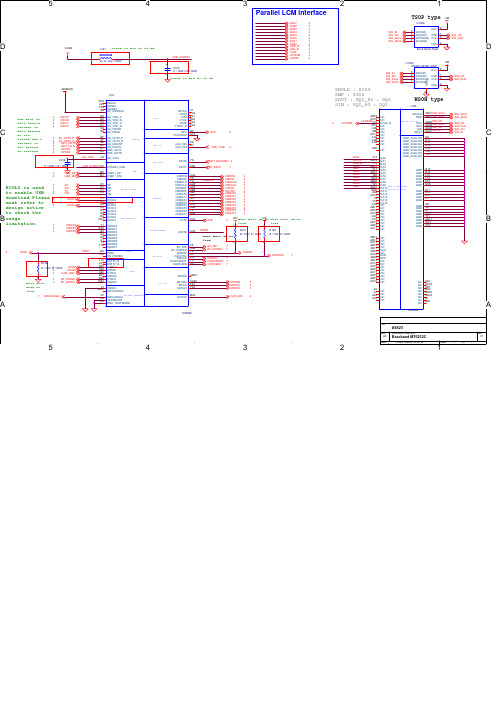
MT6252原理图资料
1
TSOP type
8 1 6 4 SQI_CE SQI_SCK VM
D
VUSB
L101
Close to pin K3 of BB
USB_AVDD33
NC & Serial Flash
D
VM
R / 0 / ohm / 0402 1 C103 C / 1000 / nF / 0402 2
U1005 MX25L12833E MXIC SQI_SI SQI_SO SQI_SIO2 SQI_SIO3 5 2 3 7 VCC DI(DQ0) DO(DQ1) CS# WP#(DQ2) CLK NC(DQ3) VSS GND 9 8 1 6 4
C
The pin1 of C218 should connect to main ground by via. Please don't connect to any ground on surface.
4 4 4 4
MICP0 MICN0 MICP1 MICN1
D2 E2 C2 C1 A3 B3 B7 A7 A6 B5 H1 H2 AU_VCM A4
Baseband MT6252C
Friday, March 16, 2012 Sheet 1 of 7
Rev V1
5
4
3
1
5
4
3
2
1
D
VBAT
TP6
TP7
TP9
TP10
D
If bead is necessary, DCR must be small
R1645 1 1 C203 C / 4700 / nF / 0603 2 1 R1646 R / 0 / ohm / 0402 2 2 R / 0 / ohm / 0402 1 VBAT_RF VBAT_DIGITAL VBAT_ANALOG VBAT_AMP B15 A13 A15 J1 J2 VBAT_RF VBAT_DIGITAL VBAT_ANALOG VBAT_SPK VBAT_SPK VBAT IN
Linear Technology LTC6363 系列精密、低功耗差分放大器 ADC 驱动器系列说

LTC6363 系列精密、低功耗差分放大器/ADC 驱动器系列特点⏹提供用户设置增益或0.5V/V、1V/V、2V/V的固定增益⏹折合到输入端噪声:2.9nV/√Hz⏹电源电流:2mA(最大值)⏹增益误差:45ppm(最大值)⏹增益误差漂移:0.5ppm/°C(最大值)⏹CMRR:94dB(最小值)⏹失调电压:100µV(最大值)⏹输入失调电流:50nA(最大值)⏹快速建立时间:720ns 至18 位,8V P–P输出⏹电源电压范围:2.8V (±1.4V) 至11V (±5.5V) ⏹差分轨到轨输出⏹输入共模范围包含地⏹低失真:115dB SFDR,2kHz 时,18V P–P⏹增益带宽积:500MHz⏹–3dB 带宽:35MHz⏹低功耗关断:20µA (V S = 3V)⏹8 引脚MSOP 和2 mm × 3mm 8 引脚DFN 封装应用⏹20 位、18 位和16 位SAR ADC 驱动器⏹单端至差分转换⏹低功耗ADC 驱动器⏹电平转换器⏹差分线路驱动器⏹电池供电仪器仪表说明LTC®6363系列包括四款全差分、低功耗、低噪声放大器,提供轨到轨输出,针对SAR ADC 驱动进行了优化。
LTC6363 是一款独立的差分放大器,其增益通常利用四个外部电阻设置。
LTC6363–0.5、LTC6363–1 和LTC6363–2 均有内部匹配电阻,形成增益分别为0.5V/V、1V/V 和2V/V 的固定增益模块。
每个固定增益放大器都有激光调整的精密片内电阻,可实现精确、超稳定的增益和出色的CMRR。
系列选型表产品型号增益配置LTC6363 用户设置LTC6363–0.5 0.5V/VLTC6363–1 1V/VLTC6363–22V/V所有注册商标和商标均属各自所有人所有。
典型应用从以地为基准的单端输入到LTC2378–20 SAR ADC 的直流耦合接口LTC6363–1 驱动LTC2378–20f IN = 2kHz,–1dBFS,131k 点FFTLTC6363 系列 绝对最大额定值(注释 1)总电源电压 (V + – V –) ........................................... 12V 输入电压(+IN 、–IN )(注释 2)LTC6363–0.5 ........ (V –) – 14.9V 至 (V +) + 14.9V LTC6363–1 ........... (V –) – 11.1V 至 (V +) + 11.1V LTC6363–2 ........... (V –) – 7.45V 至 (V +) + 7.45V 输入电流(+IN 、–IN )LTC6363(注释 3)............................................................................. ±10mA 输入电流(V OCM 、SHDN )(注释 3) .................................................. ±10mA 输出短路持续时间(注释 4) ......................................... 受散热限制 工作温度范围(注释 5)LTC6363I/LTC6363I–0.5/LTC6363I–1/ LTC6363I–2 ................................... –40°C 至 85°C LTC6363H/LTC6363H–0.5/LTC6363H–1/LTC6363H–2 ............................... –40°C 至 125°C 额定温度范围(注释 6)LTC6363I/LTC6363I–0.5/LTC6363I–1/LTC6363I–2 .................................. –40°C 至 85°C LTC6363H/LTC6363H–0.5/LTC6363H–1/LTC6363H–2............................... –40°C 至 125°C 最高结温 .............................................................. 150°C 存储温度范围 .................................. –65°C 至 150°C MSOP 引脚温度(焊接,10 秒) ................ 300°C引脚配置LTC6363LTC6363LTC6363–0.5/LTC6363–1/LTC6363–2订购信息 /product/LTC6363#orderinfo管装卷带和卷盘 器件标识* 封装说明温度范围 LTC6363IMS8#PBF LTC6363IMS8#TRPBF LTGSQ 8 引脚塑料 MSOP –40°C 至 85°C LTC6363HMS8#PBFLTC6363HMS8#TRPBFLTGSQ8 引脚塑料 MSOP –40°C 至 125°C LTC6363IMS8–0.5#PBF LTC6363IMS8–0.5#TRPBF LTGST 8 引脚塑料 MSOP –40°C 至 85°C LTC6363HMS8–0.5#PBF LTC6363HMS8–0.5#TRPBF LTGST 8 引脚塑料 MSOP –40°C 至 125°C LTC6363IMS8–1#PBF LTC6363IMS8–1#TRPBF LTGSR 8 引脚塑料 MSOP –40°C 至 85°C LTC6363HMS8–1#PBF LTC6363HMS8–1#TRPBF LTGSR 8 引脚塑料 MSOP –40°C 至 125°C LTC6363IMS8–2#PBF LTC6363IMS8–2#TRPBF LTGSS 8 引脚塑料 MSOP –40°C 至 85°C LTC6363HMS8–2#PBFLTC6363HMS8–2#TRPBFLTGSS8 引脚塑料 MSOP–40°C 至 125°CLTC6363 系列订购信息无铅表面处理卷带和卷盘(迷你型)卷带和卷盘器件标识*封装说明温度范围LTC6363IDCB#TRMPBF LTC6363IDCB#TRPBF LGVG 8 引脚(2mm × 3mm) 塑料DFN –40°C 至85°CLTC6363HDCB#TRMPBF LTC6363HDCB#TRPBF LGVG 8 引脚(2mm × 3mm) 塑料DFN –40°C 至125°CTRM = 500 片。
LTC3225中文资料

13225fTYPICAL APPLICATIONFEATURESAPPLICATIONSDESCRIPTIONChargerThe L TC ®3225 is a programmable supercapacitor charger designed to charge two supercapacitors in series to a fi xed output voltage (4.8V/5.3V selectable) from a 2.8V/3V to 5.5V input supply. Automatic cell balancing prevents overvoltage damage to either supercapacitor . No balancing resistors are required.Low input noise, low quiescent current and low external parts count (one fl ying capacitor , one bypass capacitor at V IN and one programming resistor) make the L TC3225 ideally suited for small battery-powered applications.Charging current level is programmed with an external resistor . When the input supply is removed, the L TC3225 automatically enters a low current state, drawing less than 1μA from the supercapacitors.The L TC3225 is available in a 10-lead 3mm × 2mm DFN package.nLow Noise Constant Frequency Charging of T wo Series Supercapacitorsn Automatic Cell Balancing Prevents Capacitor Overvoltage During Chargingn Programmable Charging Current (Up to 150mA)n Selectable 2.4V or 2.65V Regulation per Cell n Automatic Recharge n I VIN = 20μA in Standby Mode n I COUT < 1μA When Input Supply is Removed n No Inductorsn Tiny Application Circuit (3mm × 2mm DFN Package, All Components <1mm High)nCurrent Limited Applications with High Peak Power Loads (LED Flash, PCMCIA Tx Bursts, HDD Bursts, GPRS/GSM T ransmitter)n Backup SuppliesCharging Profi le with 30% Mismatchin Output Capacitance, C TOP < C BOTL , L T , L TC and L TM are registered trademarks of Linear Technology Corporation. All other trademarks are the property of their respective owners.OUTV IN2.8V/3V TO 5.5VSHDN 5V/DIV V COUT 2V/DIVV TOP -V BOT 200mV/DIVI VIN300mA/DIV5s/DIV 3225 TA01bV SEL = V INR PROG = 12k C TOP = 1.1F C BOT = 1.43FC TOP INITIAL VOL TAGE = 0V C BOT INITIAL VOL TAGE = 0V23225fPIN CONFIGURATIONABSOLUTE MAXIMUM RATINGSV IN , C OUT to GND .........................................–0.3V to 6V SHDN , V SEL ......................................–0.3V to V IN + 0.3VC OUT Short-Circuit Duration .............................Indefinite I VIN Continuous (Note 2) ......................................350mA I OUT Continuous (Note 2) .....................................175mA Operating Temperature Range (Note 3)....–40°C to 85°C Storage Temperature Range ...................–65°C to 125°C(Note 1)TOP VIEW 11DDB PACKAGE10-LEAD (3mm s 2mm) PLASTIC DFN C +C –CX SHDN PGOOD C OUT V IN GND PROG V SEL68791054231T JMAX = 125°C, θJA = 76°C/WEXPOSED PAD (PIN 11) MUST BE SOLDERED TO LOW IMPEDANCE GND PLANE (PIN 8) ON PCBORDER INFORMATIONELECTRICAL CHARACTERISTICS SYMBOL PARAMETERCONDITIONS MIN TYP MAX UNITSV IN-UVLO Input Supply Undervoltage LockoutHigh-to-Low ThresholdV SEL = V IN V SEL = 0l l2.652.42.752.5 2.852.6V V V IN-UVLO-HYS Input Supply Undervoltage Lockout Hysteresis V SEL = V IN V SEL = 0150140mV mVV IN Input Voltage RangeV SEL = V IN V SEL = 0V l l 32.8 5.55.5V V V COUT Charge Termination VoltageSleep Mode Threshold (Rising Edge)V SEL = V IN V SEL = 0Vl l 5.24.75.34.8 5.44.9V V V COUT-HYS Output Comparator Hysteresis 100mV V TOP/BOT Maximum Voltage Across Each of the Supercapacitors After Charging V SEL = V IN V SEL = 0V l l 2.752.5V V I Q-VIN No Load Operating Current at V IN I OUT = 0mAl 2040μA I SHDN-VIN Shutdown Current SHDN = 0V , V OUT = 0Vl 0.11μA I COUTC OUT Leakage CurrentV OUT = 5.6V , SHDN = 0VV OUT = 5.6V , Charge Pump in Sleep Mode V OUT = 5.6V , SHDN Connected to V IN with Input Supply Removedl l12341μA μA μA I VINInput Charging Current V IN = 3.6V , R PROG = 12k, C TOP = C BOT 306mA V IN = 3.6V , R PROG = 60k, C TOP = C BOT55mAThe l denotes the specifi cations which apply over the full operatingtemperature range, otherwise specifi cations are at T A = 25°C. V IN = 3.6V , C IN = 2.2μF , C FL Y = 1μF , unless otherwise specifi ed.Lead Free FinishTAPE AND REEL (MINI)TAPE AND REELPART MARKINGPACKAGE DESCRIPTIONTEMPERATURE RANGE L TC3225EDDB#TRMPBF L TC3225EDDB#TRPBF LCYR 10-Lead (3mm × 2mm) Plastic DFN –40°C to 85°CTRM = 500 pieces.Consult L TC Marketing for parts specifi ed with wider operating temperature ranges.Consult L TC Marketing for information on lead based fi nish parts.For more information on lead free part marking, go to: http://www.linear .com/leadfree/For more information on tape and reel specifi cations, go to: http://www.linear .com/tapeandreel/33225fSYMBOL PARAMETERCONDITIONSMIN TYP MAX UNITS I OUTOutput Charging CurrentV IN = 3.6V , R PROG = 12k, V OUT = 4.5V ,C TOP = C BOT125150175mA V IN = 3.6V , R PROG = 60k, V OUT = 4.5V , C TOP = C BOT26mAV PGOOD PGOOD Low Output VoltageI PGOOD = –1.6mA l 0.4V I PGOOD-LEAK PGOOD High Impedance Leakage Current V PGOOD = 5Vl 10μA V PG PGOOD Low-to-High Threshold Relative to Output Voltage Threshold l 929496%V PG-HYS PGOOD Threshold Hysteresis Relative to Output Voltage Threshold l0.251.22.5%R OL Effective Open-Loop Output Impedance (Note 4)V IN = 3.6V , V OUT = 4.5V8Ωf OSC CLK Frequencyl 0.60.9 1.5MHz V SEL , SHDN V IH Input High Voltage l 1.3VV IL Input Low Voltage l 0.4V I IH Input High Current l –11μA I ILInput Low Currentl–11μAELECTRICAL CHARACTERISTICS The l denotes the specifi cations which apply over the full operatingtemperature range, otherwise specifi cations are at T A = 25°C. V IN = 3.6V , C IN = 2.2μF , C FL Y = 1μF , unless otherwise specifi ed.Note 1: Stresses beyond those listed under Absolute Maximum Ratings may cause permanent damage to the device. Exposure to any Absolute Maximum Rating condition for extended periods may affect device reliabilty and lifetime.Note 2: Based on long-term current density limitations.Note 3: The L TC3225 is guaranteed to meet performance specifi cations from 0°C to 85°C. Specifi cations over the –40°C to 85°C operatingtemperature range are assured by design, characterization and correlation with statistical process controls. Note 4: Output not in regulation; R OL ≡ (2 • V IN – V OUT )/I OUTTYPICAL PERFORMANCE CHARACTERISTICSI OUT vs R PROGEffi ciency vs V IN(T A = 25°C, C FL Y = 1μF , C IN = 2.2μF , C TOP = C BOT , unless otherwise specifi ed)I OUT vs V OUT (R PROG = 12k)R PROG (kΩ)010I O U T (m A )60801004070603225 G0140200203050120140160V OUT (V)0I O U T (m A )2060801002451803225 G0240130.52.5 4.51.53.5120140160V IN (V)2.5E F F I C I E N C Y (%)10304050 4.5100903525 G0320 3.5354 5.560708043225fOscillator Frequency vs Supply VoltageCharge Pump Open-Loop Output Resistance vs Temperature (2V IN – V COUT )/I OUTTYPICAL PERFORMANCE CHARACTERISTICS(T A = 25°C, C FL Y = 1μF , C IN = 2.2μF , C TOP = C BOT , unless otherwise specifi ed)I OUT (mA)020457801203225 G04324060100140160106E X T R A I I N (m A )V IN (V)2.50I I N (μA )5101520303 3.54 4.53225 G055 5.525V IN20mV/DIV I VIN200mA/DIV200ns/DIV3225 G06R PROG = 12k0mACharging Profi le with Unequal Initial Output Capacitor Voltage (Initial V TOP = 1.3V , V BOT = 1V)V IN (V)2.50.88F R E Q U E N C Y (M H z )0.890.910.9233.54 4.53225 G0750.930.940.90 5.5TEMPERATURE (°C)–40R O L (Ω)6810603225 G0842579310–15103585SHDN 5V/DIV V COUT 2V/DIV V TOP -V BOT 500mV/DIVI VIN300mA/DIV2s/DIV 3225 G09V SEL = V INR PROG = 12kC TOP = C BOT = 1.1FExtra Input Current vs OutputCurrent (I VIN – 2 • I OUT )No-Load Input Current vs Supply VoltageInput Ripple and Input CurrentCharging Profi le with Unequal Initial Output Capacitor Voltage (Initial V TOP = 1V , V BOT = 1.3V)SHDN 5V/DIV V COUT 2V/DIV V TOP -V BOT 500mV/DIVI VIN300mA/DIV2s/DIV3225 G10V SEL = V INR PROG = 12kC TOP = C BOT = 1.1FSHDN 5V/DIV V COUT 2V/DIV V TOP -V BOT 200mV/DIVI VIN300mA/DIV5s/DIV 3225 G11V SEL = V INR PROG = 12k CTOP = 1.43F C BOT = 1.1FC TOP INITIAL VOL TAGE = 0V C BOT INITIAL VOL TAGE = 0VSHDN 5V/DIV V COUT 2V/DIV V TOP -V BOT 200mV/DIVI VIN300mA/DIV5s/DIV 3225 G12V SEL = V INR PROG = 12k CTOP = 1.1F C BOT = 1.43FC TOP INITIAL VOL TAGE = 0V C BOT INITIAL VOL TAGE = 0VCharging Profi le with 30%Mismatch in Output Capacitance (C TOP > C BOT )Charging Profi le with 30%Mismatch in Output Capacitance (C TOP < C BOT )PIN FUNCTIONSC+ (Pin 1): Flying Capacitor Positive Terminal. A 1μF X5R or X7R ceramic capacitor should be connected from C+ to C–.C– (Pin 2): Flying Capacitor Negative Terminal.CX (Pin 3): Midpoint of T wo Series Supercapacitors. This pin voltage is monitored and forced to track C OUT (CX = C OUT/2) during charging to achieve voltage balancing of the top and bottom supercapacitors.SHDN (Pin 4): Active Low Shutdown Input. A low on SHDN puts the L TC3225 in low current shutdown mode. Do not fl oat the SHDN pin.PGOOD (Pin 5): Open-Drain Output Status Indicator. Upon start-up, this open-drain pin remains low until the output voltage, V OUT, is within 6% (typical) of its fi nal value. Once V OUT is valid, PGOOD becomes Hi-Z. If V OUT falls 7.2% (typical) below its correct regulation level, PGOOD is pulled low. PGOOD may be pulled up through an external resistor to an appropriate reference level. This pin is Hi-Z in shutdown mode.V SEL (Pin 6): Output Voltage Selection Input. A logic low at V SEL sets the regulated C OUT to 4.8V; a logic high sets the regulated C OUT to 5.3V. Do not fl oat the V SEL pin. PROG (Pin 7): Charging Current Programming Pin. A resis-tor connected between this pin and GND sets the charging current. (See Applications Information section).GND (Pin 8): Charge Pump Ground. This pin should be connected directly to a low impedance ground plane.V IN (Pin 9): Power Supply for the L TC3225. V IN should be bypassed to GND with a low ESR ceramic capacitor of more than 2.2μF.C OUT (Pin 10): Charge Pump Output Pin. Connect C OUT to the top plate of the top supercapacitor. C OUT provides charge current to the supercapacitors and regulates the fi nal voltage to 4.8V/5.3V.Exposed Pad (Pin 11): This pad must be soldered to a low impedance ground plane for optimum thermal performance.53225fSIMPLIFIED BLOCK DIAGRAMTOPBOT3225 F01Figure 163225fOPERATIONThe L TC3225 is a dual cell supercapacitor charger. Its unique topology maintains a constant output voltage with programmable charging current. Its ability to maintain equal voltages on both cells while charging protects the supercapacitors from damage that is possible with other charging methods, without the use of external balancing resistors. The L TC3225 includes an internal switched capacitor charge pump to boost V IN to a regulated output voltage. A unique architecture maintains relatively constant input current for the lowest possible input noise. The basic charger circuit requires only three external components. Normal Charge CycleOperation begins when the SHDN pin is pulled above 1.3V. The C OUT pin voltage is sensed and compared with a preset voltage threshold using an internal resistor divider and a comparator. The preset voltage threshold is 4.8V/5.3V selectable with the V SEL pin. If the voltage at the C OUT pin is lower than the preset voltage threshold, the oscillator is enabled. The oscillator operates at a typical frequency of 0.9MHz. When the oscillator is enabled, the charge pump operates charging up C OUT. The input current drawn by the internal charge pump ramps up at approximately 20mA/μs each time the charge pump starts up from shutdown. Once the output voltage is charged to the preset voltage threshold, the part shuts down the internal charge pump and enters into a low current state. In this state, the L TC3225 consumes only about 20μA from the input supply. The current drawn from C OUT is approximately 2μA. Automatic Cell BalancingThe L TC3225 constantly monitors the voltage across both supercapacitors while charging. When the voltage across the supercapacitors is equal, both capacitors are charged with equal currents. If the voltage across one supercapacitor is lower than the other, the lower supercapacitor’s charge current is increased and the higher supercapacitor’s charge current is decreased. The greater the difference between the supercapacitor voltages, the greater the difference in charge current per capacitor. The charge currents can increase or decrease as much as 50% to balance the volt-age across the supercapacitors. When the cell voltages are balanced, the supercapacitors are charged at a rate of approximately:I ICOUT VIN=12•If the leakage currents or capacitances of the two su-percapacitors are mismatched enough that varying the charging current is not suffi cient to balance their volt-ages, the L TC3225 stops charging the capacitor with the higher voltage until they are again balanced. This feature protects either capacitor from experiencing an overvoltage condition.Shutdown ModeAsserting SHDN low causes the L TC3225 to enter shut-down mode. When the charge pump is fi rst disabled, the L TC3225 draws approximately 1μA of supply current from V IN and C OUT. After V OUT is discharged to 0V, the current from V IN drops to less than 1μA. With SHDN connected to V IN, the output sinks less than 1μA when the input sup-ply is removed. Since the SHDN pin is a high impedance CMOS input, it should never be allowed to fl oat. Output Status Indicator (PGOOD)During shutdown, the PGOOD pin is high impedance. When the charge cycle starts, an internal N-channel MOSFET pulls the PGOOD pin to ground. When the output voltage, V OUT, is within 6% (typical) of its fi nal value, the PGOOD pin becomes high impedance, but charge current continues to fl ow until V OUT crosses the charge termination voltage. When V OUT drops 7% below the charge termination volt-age, the PGOOD pin again pulls low.Current Limit/Thermal ProtectionThe L TC3225 has built-in current limit as well as overtem-perature protection. If the PROG pin is shorted to ground, a protection circuit automatically shuts off the internal charge pump. At higher temperatures, or if the input voltage is high enough to cause excessive self-heating of the part, the thermal shutdown circuitry shuts down the charge pump once the junction temperature exceeds approximately 150°C. It will enable the charge pump once the junction temperature drops back to approximately 135°C. The L TC3225 is able to cycle in and out of thermal shutdown indefi nitely without latch-up or damage until the overcurrent condition is removed.73225f83225fAPPLICATIONS INFORMATIONProgramming Charge CurrentThe charging current is programmed with a single resistor connecting the PROG pin to ground. The program resistor and the input/output charge currents are calculated using the following equations:I V R I IVIN PROGOUTVIN ==36002(with matched outp p ut capacitors)An R PROG resistor value of 2k or less (i.e., short circuit) causes the L TC3225 to enter overcurrent shutdown mode. This mode prevents damage to the part by shutting down the internal charge pump.Power Effi ciencyThe power effi ciency (η) of the L TC3225 is similar to that of a linear regulator with an effective input voltage of twice the actual input voltage. In an ideal regulating voltage doubler the power effi ciency is given by:η222xIDEAL OUT IN OUT OUT IN OUT OUTI P P V I V I V V ===••NAt moderate to high output power the switching losses and quiescent current of the L TC3225 are negligible and the above expression is valid. For example, with V IN = 3.6V , I OUT = 100mA and V OUT regulated to 5.3V , the measured effi ciency is 71.2% which is in close agreement with the theoretical 73.6% calculation.Effective Open-Loop Output Resistance (R OL )The effective open-loop output resistance (R OL ) of a charge pump is an important parameter that describes the strength of the charge pump. The value of this parameter depends on many factors including the oscillator frequency (f OSC ), value of the fl ying capacitor (C FL Y ), the non-overlap time,the internal switch resistances (R S ) and the ESR of the external capacitors. Output Voltage ProgrammingThe L TC3225 has a V SEL input pin that allows the user to set the output threshold voltage to either 4.8V or 5.3V by forcing a low or high at the V SEL pin respectively.Charging Time EstimationThe estimated charging time when the initial voltage across the two output supercapacitors is equal is given by the equation:t C V V I CHRG OUT COUT INIOUT=()•–where C OUT is the series output capacitance, V COUT is thevoltage threshold set by the V SEL pin, V INI is the initial voltage at the C OUT pin and I OUT is the output charging current given by:I V R OUT PROG=1800When the charging process starts with unequal initialvoltages across the output supercapacitors, only the ca-pacitor with the lower voltage level is charged; the other capacitor is not charged until the voltages equalize. This extends the charging time slightly. Under the worst-case condition, whereby one capacitor is fully depleted while the other remains fully charged due to signifi cant leakage current mismatch, the charging time is about 1.5 times longer than normal. Thermal ManagementFor higher input voltages and maximum output current, there can be substantial power dissipation in the L TC3225. If the junction temperature increases above approximately150°C, the thermal shutdown circuitry automatically deactivates the output. To reduce the maximum junction temperature, a good thermal connection to the PC board is recommended. Connecting the GND pin (Pin 8) and the Exposed Pad (Pin 11) of the DFN package to a ground plane under the device on two layers of the PC board can reduce the thermal resistance of the package and PC board considerably.V IN Capacitor SelectionThe type and value of C IN controls the amount of ripple present at the input pin (V IN). To reduce noise and ripple, it is recommended that low equivalent series resistance (ESR) multilayer ceramic chip capacitors (MLCCs) be used for C IN. Tantalum and aluminum capacitors are not recommended because of their high ESR.The input current to the L TC3225 is relatively constant dur-ing both the input charging phase and the output charging phase but drops to zero during the clock non-overlap times. Since the non-overlap time is small (~40ns) these missing “notches” result in only a small perturbation on the input power supply line. Note that a higher ESR capacitor, such as a tantalum, results in higher input noise. Therefore, ceramic capacitors are recommended for their exceptional ESR performance. Further input noise reduction can be achieved by powering the L TC3225 through a very small series inductor as shown in Figure 2.A 10nH inductor will reject the fast current notches, thereby presenting a nearly constant current load to the input power supply. For economy, the 10nH inductor can be fabricated on the PC board with about 1cm (0.4") of PC board trace.Flying Capacitor SelectionWarning: Polarized capacitors such as tantalum or alumi-num should never be used for the fl ying capacitor since it s volt age can reverse upon st art-up of t he LTC3225. Low ESR ceramic capacitors should always be used for the fl ying capacitor.The fl ying capacitor controls the strength of the charge pump. In order to achieve the rated output current, it is necessary to use at least 0.6μF of capacitance for the fl ying capacitor.The effective capacitance of a ceramic capacitor varies with temperature and voltage in a manner primarily determined by its formulation. For example, a capacitor made of X5R or X7R material retains most of its capacitance from –40°C to 85°C whereas a Z5U or Y5V type capacitor loses considerable capacitance over that range. X5R, Z5U and Y5V capacitors may also have a poor voltage coeffi cient causing them to lose 60% or more of their capacitance when the rated voltage is applied. Therefore, when com-paring different capacitors, it is often more appropriate to compare the amount of achievable capacitance for a given case size rather than comparing the specifi ed capacitance value. For example, over rated voltage and temperature conditions, a 4.7μF 10V Y5V ceramic capacitor in a 0805 case may not provide any more capacitance than a 1μF 10V X5R or X7R capacitor available in the same 0805 case. In fact, over bias and temperature range, the 1μF 10V X5R or X7R provides more capacitance than the 4.7μF 10V Y5V capacitor. The capacitor manufacturer’s data sheet should be consulted to determine what value of capacitor is needed to ensure minimum capacitance values are met over operating temperature and bias voltage.V INFigure 2. 10nH Inductor Used for Input Noise Reduction APPLICATIONS INFORMATION93225f103225fTYPICAL APPLICATIONTable 1 contains a list of ceramic capacitor manufacturers and how to contact them.Table 1. Capacitor ManufacturersAVX Kemet Murata Taiyo Yuden Vishay TDKLayout ConsiderationsDue to the high switching frequency and high transient currents produced by the L TC3225, careful board layout is necessary for optimum performance. An unbroken ground plane and short connections to all the external capacitors improves performance and ensures proper regulation under all conditions.The voltages on the fl ying capacitor pins C + and C – have very fast rise and fall times. The high dv/dt values on these pins can cause energy to capacitively couple to adjacent printed circuit board traces. Magnetic fi elds can also be generated if the fl ying capacitors are far from the part (i.e. the loop area is large). To prevent capacitive energy transfer , a Faraday shield may be used. This is a grounded PC trace between the sensitive node and the L TC3225 pins. For a high quality AC ground it should be returned to a solid ground plane that extends all the way to the L TC3225.Table 2. Supercapacitor ManufacturersCAP-XX NESS CAP Maxwell Bussmann AVXAPPLICATIONS INFORMATION5V Supercapacitor Backup SupplyO VLTC3225113225fInformation furnished by Linear Technology Corporation is believed to be accurate and reliable. However , no responsibility is assumed for its use. Linear Technology Corporation makes no representa-tion that the interconnection of its circuits as described herein will not infringe on existing patent rights.PACKAGE DESCRIPTIONDDB Package10-Lead Plastic DFN (3mm × 2mm)(Reference L TC DWG # 05-08-1722 Rev Ø)NOTE:1. DRAWING CONFORMS TO VERSION (WECD-1) IN JEDEC PACKAGE OUTLINE M0-2292. DRAWING NOT TO SCALE3. ALL DIMENSIONS ARE IN MILLIMETERS4. DIMENSIONS OF EXPOSED PAD ON BOTTOM OF PACKAGE DO NOT INCLUDEMOLD FLASH. MOLD FLASH, IF PRESENT, SHALL NOT EXCEED 0.15mm ON ANY SIDE 5. EXPOSED PAD SHALL BE SOLDER PLATED6. SHADED AREA IS ONLY A REFERENCE FOR PIN 1 LOCATION ON THE TOP AND BOTTOM OF PACKAGEBOTTOM VIEW—EXPOSED PAD(DDB10) DFN 0905 REV ØPIN 1R = 0.20 OR 0.25s 45o CHAMFERRECOMMENDED SOLDER PAD PITCH AND DIMENSIONSLTC3225123225fLinear Technology Corporation1630 McCarthy Blvd., Milpitas, CA 95035-7417(408) 432-1900 ● FAX: (408) 434-0507 ● © LINEAR TECHNOLOGY CORPORA TION 2008LT 0508 • PRINTED IN USARELATED PARTSTYPICAL APPLICATIONPART NUMBERDESCRIPTIONCOMMENTSL TC1751-3.3/L TC1751-5Micropower 5V/3.3V Doubler Charge Pumps I Q = 20μA, Up to 100mA Output, SOT-23 Package L TC1754-3.3/L TC1754-5Micropower 5V/3.3V Doubler Charge Pumps I Q = 13μA, Up to 50mA Output, SOT-23 Package L TC3200Constant Frequency Doubler Charge Pump Low Noise, 5V Output or AdjustableL TC3203/L TC3203B/L TC3203B-1/L TC3203-1500mA Low Noise High Effi ciency Dual Mode Step-Up Charge PumpsV IN : 2.7V to 5.5V , 3mm × 3mm 10-Lead DFN Package L TC3204/L TC3204B-3.3/L TC3204-5Low Noise Regulating Charge Pumps Up to 150mA (L TC3204-5), Up to 50mA (L TC3204-3.3)L TC3221/L TC3221-3.3/L TC3221-5Micropower Regulated Charge Pump Up to 60mA OutputL TC3240-3.3/L TC3240-2.5Step-Up/Step-Down Regulated Charge Pumps Up to 150mA OutputL T ®3420/L T3420-1 1.4A/1A Photofl ash Capacitor Charger with Automatic Top-Off Charges 220μF to 320V in 3.7 Seconds from 5V , V IN : 2.2V to 16V , I SD < 1μA, 10-Lead MS PackageL T3468/L T3468-1/L T3468-21.4A/1A/0.7A, Photofl ash Capacitor Charger V IN :2.5V to 16V , Charge Time = 4.6 Seconds for the L T3468 (0V to 320V , 100μF , V IN =3.6V), I SD < 1μA, ThinSOT TM PackageL TC3484-0/L TC3484-1/ L TC3484-21.4A/0.7A/1A, Photofl ash Capacitor ChargerV IN : 1.8V to 16V , Charge Time = 4.6 Seconds for the L T3484-0 (0V to 320V , 100μF , V IN = 3.6V), I SD < 1μA, 2mm × 3mm 6-Lead DFN PackageL T3485-0/L T3485-1/ L T3485-2/L T3485-31.4A/0.7A/1A/2A Photofl ash Capacitor Chargerwith Output Voltage Monitor and Integrated IGBTV IN : 1.8V to 10V , Charge Time = 3.7 Seconds for the L T3485-0 (0V to 320V , 100μF , V IN = 3.6V), I SD < 1μA, 3mm × 3mm 10-Lead DFN Driver L T3750Capacitor Charger Controller Charges Any Size Capacitor , 10-Lead MS PackageThinSOT is a trademark of Linear Technology Corporation.V BIAS 3.3V V IN 12VGNDGNDL T3740HIGH EFFICIENCY D1CSHD6-40C 12V Supercapacitor Backup Supply。
放大器模块常用芯片简介
放大器模块常用芯片简介MAX4106:⑴低成本,高速,单电源运算放大器。
⑵满摆幅输出的运算放大器,-3db带宽为150MHZ,可以采用正负5V或者单电源供电,⑶采用Umax-8和SO-8封装。
THS3092:⑴高速电流反馈双运算放大器芯片⑵160MHZ(G=5,RL=100)电源电源范围正负5-15V. ⑶采用SOIC-8和TSSOP-14封装。
AD624:⑴高精度,低噪声仪表放大器芯片⑵主要用于设计低电平传感器(负荷传感器,应变计和压力传感器)⑶可用于高速数据采集应用。
AD603⑴90MHZ带宽,增益程控可调的集成运算放大器芯片⑵增益与控制电压成线性关系,增益变化范围40dB ⑶采用SOIC-8和CERDIP-8封装AD8055;⑴电压反馈型放大器芯片⑵该芯片0.1dB增益平坦度为40MHZ,带宽达300MHZ,压摆率为1400V/us,建立时间为20ns,适合各种高速应用。
⑶采用正负5V双电源或+12V单电源,仅需5mA的电源电流,负载电流可达60mA,工作温度-40―+125度。
⑷采用PDIP-8,SOIC-8和SOT-23-5封装 AD811⑴视频运算放大器芯片⑵具有高速,高频,宽频带和低噪声等优异特性⑶具有140MHZ带宽,120MHZ带宽,35MHZ带宽,2500V/us摆率,建立时间25ns⑷采用8引脚SOIC(R-8),16,20引脚等ICL7650/53: ⑴运算放大器芯片⑵具有极低的输入失调电压,整个工作温度范围(约100度)内只有1Uv,失调电压的温漂为0.01Uv/度,开环增益极高,转换率SR=2.5V/us………⑶电源电压范围V+到V-为4.5-16V.LM386⑴音频功率放大器⑵工作电压4-12V,5-18V静态功耗约4mA可用于电池供电,电压增益范围20-200,可调;⑶采用8引线双列直插式,贴片式封装 TEA2050⑴双声道立体声音频功率放大集成电路芯片⑵工作电源电压3-15V,工作电压6-9V,输出功率与电源电压和扬声器阻抗有关⑶采用POWERDIP16和SO20封装 LTC1068⑴开关电容滤波器芯片⑵它包含4个同样的二阶滤波器。
LTC2655特性-应用
LTC2655特性/应用
描述
LTC®2655是一个4 通道、I2C、16 位/ 12 位、轨至轨DAC 系列,具有集成10ppm/?C 最大值基准。
这些DAC 具有内置的高性能、轨至轨输出缓冲器,并保证具有单调特性。
LTC2655-L 具有一个 2.5V 的全标度输出和集成基准,并采用 2.7V 至 5.5V 的单工作电源。
LTC2655-H 具有一个 4.096V 的全标度输出和集成基准,并采用 4.5V 至 5.5V 的单工作电源。
每个DAC 也可以采用一个外部基准来运作,该外部基准负责将DAC 全标度输出设定为外部基准电压的两倍。
这些器件采用二线式I2C 兼容型串行接口。
LTC2655 工作于标准模式(最大时钟频率为100kHz) 和快速模式(最大时钟频率为400kHz)。
LTC2655 包括一个受控于PORSEL 引脚的上电复位电路。
如果PORSEL 引脚连接至GND,则DAC 在上电时被复位至零标度。
如果PORSEL 引脚连接至VCC,则DAC 在上电时将被复位至中间标度。
特点
●集成10ppm/uC 最大值基准
●最大INL 误差:±4LSB (在16 位)
●在整个温度范围内保证单调
●可选择的内部或外部基准
●2.7V至5.5V 电源范围(LTC2655-L)
●集成基准缓冲器
●DAC之间的超低串扰(1nVus)
●上电复位至零标度/中间标度。
proteus元件分类及子类
杂类(miscellaneous)
可动态显示充放电电容
音响专用轴线电容
轴线聚苯烯电容
轴线聚苯乙烯电容
陶瓷圆片电容
去耦片状电容
普通电容
高温径线电容
高温轴线电解电容
金属化聚酯膜电容
金属化聚烯电容
金属化聚烯膜电容
小型电解电容
多层金属化聚酯膜电容 聚酯膜电容 镍栅电容 无极性电容 聚酯层电容 径线电解电容 树脂蚀刻电容 钽珠电容 可变电容 VX轴线电解电容 音频接口 D型接口 双排插座 插头 PCB转换器 带线 单排插座 连线端子 杂类(miscellaneous) 模数转换器 数模转换器 采样保持器 温度传感器 断点触发器
开关器件(switching devices) 热阴极电子管(thermionic valves)
转换器(transducers) 晶体管(transistors)
二路运放 三路运放 四路运放 八路运放 理想运放 大量使用的运放 7段数码管 英文字符与数字符号液晶显示器 条形显示器 点阵显示屏 图形液晶 灯泡 液晶控制器 液晶面板显示器 发光二极管 光耦元件 串行液晶 无子分类 0.6w金属膜电阻 10w绕线电阻 2w金属膜电阻 3w金属膜电阻 7w金属膜电阻 通用电阻符号 高压电阻 负温度系数热敏电阻 排阻 滑动变阻器 可变电阻 触发器 门电路 电源 无子分类 键盘 普通继电器 专用继电器 按键与拨码开关 双端交流开关元件 普通开关元件 可控硅 三端可控硅 三极真空管 二极真空管 四极真空管 五极真空管 压力传感器 温度传感器 双极性晶体管 普通晶体管 绝缘栅场效应管 结型场效应管 金属-氧化物半导体场效应管 射频功率LDMOS晶体管 射频功率VDMOS晶体管
ISL6251(笔记本)电池充放电管理芯片引脚定义(图)
ISL6251AHRZ (笔记本)电池充放电管理芯片引脚定义21,22脚CSOP/CSON:是电池的充电电流感应正/负输入。
在CSOP的差动电压和CSON是用于检测电池的充电电流,并与充电电流限制门限调节充电电流。
该CSON管脚也可以用作电池的反馈电压来执行电压调节。
19,20脚CSIP/CSIN: 是AC适配器电流传感正/负输入。
CSIP的两端的差分电压和CSIN是用于检测AC适配器电流,并与AC适配器电流限制相比,调节AC适配器电流。
24脚DCIN: 是内部5V LDO输入。
它连接到AC适配器的输出。
连接DCIN一个0.1μF的陶瓷电容。
2脚ACSET:是一个AC适配器检测输入。
连接到从适配器输入电阻分压器。
23脚CACPRN:是AC适配器开漏输出。
ACPRN是低电平时ACSET比通常1.26V较高,高电平时ACSET比一般1.26V低。
3脚EN:是充电使输入。
连接中文高使充电控制功能,连接中文的充电功能低禁用。
使用的热敏电阻来检测并暂停热电池充电。
7脚ICM:是适配器的电流输出。
该引脚输出产生的电压成正比适配器的电流。
13脚PGND:是电源地。
连接PGND到的低侧MOSFET栅极驱动器低电压端MOSFET源。
1脚VDD:是一个内部LDO输出电源IC的模拟电路。
连接一个1μF陶瓷电容接地。
15脚VDDP:是低端MOSFET栅极驱动器电源电压。
4.7Ω电阻连接到VDD和1μF陶瓷电容,电源地。
5脚ICOMP:是一个电流环误差放大器输出。
6脚VCOMP:是一个循环放大器的输出电压。
4脚CELLS:这个引脚用于选择电池电压。
细胞=内径为4型电池组,电池=接地为3S号电池,电池=浮法为2秒电池组。
11脚V ADJ:调整电池的稳压电压。
V ADJ =参考电压为4.2V的5%; V ADJ =为4.2V/cell浮动; V ADJ =接地为4.2V的5%。
连接到电阻分压器进行编程至4.2V之间,5%和5%的预期4.2V的电池电压。
OPA类TI免费芯片汇集
OPA1013- 精密单电源双路运算放大器OPA1013CN8P 所有无铅库存$0.00OPA124- 低噪声的精密差动运算放大器OPA124U D 所有无铅库存$0.00OPA124UA D 所有无铅库存$0.00OPA129- 超低偏置电流差动运算放大器OPA129U D 所有无铅库存$0.00OPA129UB D 所有无铅库存$0.00OPA131- 通用 FET- 输入运算放大器OPA131UA D 所有无铅库存$0.00OPA1602- OPA1602、OPA1604 SoundPlus 高性能、双极输入音频运算放大器OPA1602AID D 暂时缺货$0.00OPA1642- Sound-Plus 高性能、JFET 输入音频运算放大器OPA1642AID D 暂时缺货$0.00OPA2130- 低功耗精密 FET 输入运算放大器OPA2130UA D 所有无铅库存$0.00OPA2137- 低成本 FET 输入运算放大器OPA2137P P 所有无铅库存$0.00OPA2141- 10MHz 单电源低噪声 JFET 精密放大器 ]]OPA2141AID D 所有无铅库存$0.00OPA2141AIDR D 所有无铅库存$0.00OPA2227- 高精度、低噪声运算放大器OPA2227P P 所有无铅库存$0.00OPA2227U D 所有无铅库存$0.00OPA2227UA D 所有无铅库存$0.00OPA2228- 高精度低噪声运算放大器OPA2228P P 所有无铅/绿色环保库存$0.00OPA2228PA P 所有无铅库存$0.00OPA2228U D 所有无铅库存$0.00OPA2228UA D 所有无铅库存$0.00OPA2333-HT- 1.8V 微功耗 CMOS 运算放大器OPA2333SJD JD 所有无铅无偏好** 库存$0.00OPA2334- 最大漂移0.05uV/℃ 的单电源 CMOS 运算放大器OPA2334AIDGST DGS 所有无铅/绿色环保库存$0.00 OPA2335- 最大漂移0.05uV/℃ 的单电源 CMOS 运算放大器OPA2335AIDGKT DGK 所有无铅库存$0.00 OPA2335AIDR D 所有无铅/绿色环保库存$0.00 OPA2338- MicroSIZE、单电源 CMOS 运算放大器微放大器系列OPA2338EA/250DCN 所有无铅/绿色环保库存$0.00OPA2354- 250MHz 轨至轨 I/O CMOS 双路运算放大器OPA2354AIDDA DDA 所有无铅库存$0.00 OPA2354AIDGKT DGK 所有无铅库存$0.00 OPA2376- 精密、低噪声、低静态电流运算放大器OPA2376AIDR D 所有无铅/绿色环保库存$0.00 OPA2376AIYZDT YZD 所有无铅/绿色环保库存$0.00 OPA2380- 高速精确互阻抗放大器OPA2380AIDGKT DGK 所有无铅/绿色环保库存$0.00 OPA2652- SpeedPlus(TM) 双路 700MHz 电压反馈运算放大器OPA2652U D 所有无铅/绿色环保库存$0.00 OPA2684- 双路低功耗电流反馈运算放大器OPA2684ID D 暂时缺$0.00货OPA2690- 具有禁用功能的双路宽带电压反馈运算放大器OPA2690ID D 所有无铅/绿色环保库存$0.00 OPA2703- 12V CMOS 轨至轨 I/O 运算放大器OPA2703UA D 所有无铅/绿色环保库存$0.00 OPA2703UAG4 D 所有无铅库存$0.00 OPA2704- 12V CMOS 轨至轨 I/O 运算放大器OPA2704EA/250DGK 所有无铅库存$0.00 OPA2704EA/250G4 DGK 所有无铅库存$0.00 OPA2704PA P 所有无铅/绿色环保库存$0.00 OPA2890- 具有禁用功能的双路低功耗宽带电压反馈运算放大器OPA2890ID D 所有无铅/绿色环保库存$0.00 OPA320- 20MHz、0.9pA Ib、RRIO、精密 CMOS 运算放大器OPA320AIDBVT DBV 所有无铅库存$0.00 OPA320SAIDBVT DBV 暂时缺$0.00货OPA3355- 具有关断状态的 2.5V 200MHz 的 GBW CMOS 三路运算放大器OPA3355EA/250PW 所有无铅/绿色环保库存$0.00 OPA3355UA D 所有无铅库存$0.00 OPA337- MicroAmplifier(TM) 系列微型单电源 CMOS 运算放大器OPA337NA/250DBV 所有无铅/绿色环保库存$0.00 OPA343- MicroAmplifier(TM) 系列单电源轨至轨运算放大器OPA343UA D 所有无铅/绿色环保库存$0.00 OPA347- 微功耗轨至轨运算放大器OPA347NA/250DBV 所有无铅/绿色环保库存$0.00 OPA347PA P 所有无铅/绿色环保暂时缺$0.00货OPA347SA/250DCK 所有无铅库存$0.00 OPA353- MicroAmplifier(TM) 系列高速单电源轨至轨运算放大器OPA353UA D 所有无铅/绿色环保库存$0.00 OPA364- 1.8V、高 CMR、RRIO 运算放大器OPA364AID D 所有无铅/绿色环保库存$0.00 OPA364AIDBVT DBV 所有无铅/绿色环保库存$0.00 OPA364IDBVT DBV 所有无铅/绿色环保库存$0.00 OPA3692- 具有禁用功能的三路宽带固定增益缓冲器OPA3692ID D 所有无铅/绿色环保库存$0.00 OPA3692IDBQT DBQ 所有无铅/绿色环保库存$0.00 OPA379- 1.8V、2.9µA、90kHz、轨至轨 I/O 运算放大器OPA379AIDCKT DCK 所有无铅/绿色环保库存$0.00 OPA380- 高速精密互阻抗放大器OPA380AIDGKT DGK 所有无铅库存$0.00 OPA4134- SoundPlus(TM) 高性能音频运算放大器OPA4134UA D 所有无铅库存$0.00 OPA4170- 36V、微功耗、轨至轨输出、四路、通用运算放大器OPA4170AID D 所有无铅库存$0.00 OPA4170AIPW PW 所有无铅库存$0.00 OPA4350- MicroAmplifier(TM) 系列高速单电源轨至轨运算放大器OPA4350EA/250DBQ 所有无铅/绿色环保库存$0.00 OPA4350UA D 所有无铅/绿色环保库存$0.00 OPA4353- MicroAmplifier(TM) 系列高速单电源轨至轨运算放大器OPA4353UA D 所有无铅/绿色环保库存$0.00 OPA4364- 1.8V、高 CMR、RRIO 运算放大器OPA4364AID D 所有无铅/绿色环保库存$0.00 OPA4704- 12V CMOS 轨至轨 I/O 运算放大器OPA4704UA D 所有无铅库存$0.00 OPA548- 高电压大电流运算放大器,出色的输出摆幅OPA548FKTWT KTW 所有无铅/绿色环保库存$0.00 OPA548T KVT 所有无铅/绿色环保库存$0.00 OPA561- 大电流运算放大器OPA561PWP PWP 所有无铅/绿色环保库存$0.00 OPA606- Wide-Bandwidth Difet(R) 运算放大器OPA606KP P 所有无铅/绿色环保库存$0.00 OPA656- 宽带单位增益稳定 FET 输入运算放大器OPA656N/250DBV 所有无铅库存$0.00 OPA656N/250G4DBV 所有无铅库存$0.00 OPA656NB/250DBV 所有无铅库存$0.00 OPA656U D 所有无铅库存$0.00 OPA656UB D 所有无铅库存$0.00 OPA694- 宽带、低功耗、电流反馈放大器OPA694ID D 所有无铅库存$0.00OPA1013- 精密单电源双路运算放大器OPA1013CN8P 所有无铅库存$0.00 OPA121- 低成本的精密差动运算放大器OPA121KU D 所有无铅库存$0.00 OPA124- 低噪声的精密差动运算放大器OPA124U D 所有无铅库存$0.00 OPA124UA D 所有无铅库存$0.00 OPA129- 超低偏置电流差动运算放大器OPA129U D 所有无铅库存$0.00 OPA129UB D 所有无铅库存$0.00 OPA130- 低功耗精密 FET 输入运算放大器OPA130UA D 所有无铅库存$0.00 OPA131- 通用 FET- 输入运算放大器OPA131UA D 所有无铅库存$0.00 OPA132- 高速 FET 输入运算放大器OPA132U D 所有无铅库存$0.00 OPA132UA D 所有无铅库存$0.00 OPA134- SoundPlus(TM) 高性能音频运算放大器OPA134PA P 所有无铅/绿色环保库存$0.00OPA134UA D 所有无铅无偏好** 库存$0.00OPA137- 低成本 FET 输入运算放大器OPA137P P 所有无铅无偏好** 库存$0.00OPA137PA P 库存$0.00 OPA140- 11MHz 单电源、低噪声、精密轨至轨输出 JFET 放大器OPA140AID D 所有无铅库存$0.00 OPA140AIDBVT DBV 所有无铅库存$0.00 OPA140AIDGKT DGK 所有无铅库存$0.00 OPA141- 10MHz 单电源低噪声 JFET 精密放大器OPA141AID D 所有无铅无偏好** 库存$0.00OPA141AIDGKT DGK 所有无铅库存$0.00OPA1602- OPA1602、OPA1604 SoundPlus 高性能、双极输入音频运算放大器OPA1602AID D 暂时缺货$0.00OPA1611- 1.1nV/√Hz 噪声、低功耗精密运算放大器OPA1611AID D 所有无铅库存$0.00OPA1612- 1.1nV/√Hz 噪声、低功耗精密运算放大器OPA1612AID D 所有无铅库存$0.00OPA1632- 全差动 I/O 音频放大器OPA1632D D 所有无铅/绿色环保库存$0.00OPA1632DR D 所有无铅库存$0.00OPA1641- Sound-Plus 高性能、JFET 输入音频运算放大器OPA1641AID D 所有无铅库存$0.00OPA1642- Sound-Plus 高性能、JFET 输入音频运算放大器OPA1642AID D 暂时缺货$0.00OPA1644- OPA1641/1642/1644 SoundPLUS™ 高性能 JFET 输入音频运算放大器OPA1644AID D 所有无铅无偏好** 库存$0.00OPA1654- Sound Plus 低噪声和低失真通用 FET 输入音频运算放大器OPA1654AID D 所有无铅库存$0.00OPA1654AIPW PW 所有无铅库存$0.00OPA1662-Q1- 汽车类 Sound Plus、低功耗、低噪声和低失真音频运算放大器OPA1662AIDGKRQ1 DGK 所有无铅库存$0.00OPA1662AIDRQ1 D 库存$0.00OPA1664- Sound Plus 低功耗、低噪声和低失真音频运算放大器OPA1664AID D 所有无铅库存$0.00OPA1664AIPW PW 所有无铅无偏好** 库存$0.00OPA170- 采用微型封装的 36V、微功耗、轨至轨输出、通用运算放大器OPA170AID D 所有无铅库存$0.00OPA170AIDBVT DBV 所有无铅库存$0.00OPA170AIDRLR DRL 所有无铅库存$0.00OPA170AIDRLT DRL 所有无铅库存$0.00OPA171- 采用微型封装的 36V 通用低功耗 RRO 运算放大器OPA171AID D 所有无铅库存$0.00OPA171AIDBVT DBV 所有无铅库存$0.00OPA171AIDRLT DRL 所有无铅库存$0.00OPA177- 精密运算放大器OPA177FP P 库存$0.00OPA177GP P 所有无铅库存$0.00OPA177GS D 所有无铅库存$0.00OPA177GS/2K5 D 所有无铅库存$0.00OPA188- 0.03μV/°C、6μV Vos、低噪声、轨至轨输出、36V 零漂移运算放大器OPA188AIDGKT DGK 所有无铅库存$0.00OPA1S2385- 具有集成开关和缓冲器的 200-MHz CMOS 跨阻放大器 (TIA)OPA1S2385IDRCT DRC 暂时缺货$0.00OPA211- 1.1nV/(sqrt)Hz Noise, Low Power, Precision Operational Amplifier in DFN-8 Pkg OPA211AIDR D 所有无铅/绿色环保库存$0.00OPA211ID D 所有无铅/绿色环保库存$0.00OPA211IDRGT DRG 所有无铅/绿色环保库存$0.00 OPA2130- 低功耗精密 FET 输入运算放大器OPA2130UA D 所有无铅库存$0.00 OPA2131- 通用 FET 输入运算放大器OPA2131UA D 所有无铅无偏好** 库存$0.00OPA2131UJ D 所有无铅库存$0.00 OPA2132- 高速 FET 输入运算放大器OPA2132P P 库存$0.00OPA2132PA P 所有无铅无偏好** 库存$0.00OPA2132U D 所有无铅无偏好** 库存$0.00OPA2132UA D 所有无铅库存$0.00OPA2134- SoundPlus(TM) 高性能音频运算放大器OPA2134PA P 所有无铅库存$0.00OPA2134UA D 所有无铅库存$0.00OPA2137- 低成本 FET 输入运算放大器OPA2137P P 所有无铅库存$0.00OPA2141- 10MHz 单电源低噪声 JFET 精密放大器 ]]OPA2141AID D 所有无铅库存$0.00OPA2141AIDR D 所有无铅库存$0.00OPA2170- 采用微型封装的 36V、微功耗、轨至轨输出、双路通用运算放大器OPA2170AID D 暂时缺货$0.00OPA2170AIDGK DGK 所有无铅库存$0.00OPA2171- 采用微型封装的 36V 通用低功耗 RRO 运算放大器OPA2171AID D 所有无铅库存$0.00OPA2171AIDCUT DCU 所有无铅库存$0.00OPA2227- 高精度、低噪声运算放大器OPA2227P P 所有无铅库存$0.00OPA2227U D 所有无铅库存$0.00OPA2227UA D 所有无铅库存$0.00OPA2228- 高精度低噪声运算放大器OPA2228P P 所有无铅/绿色环保库存$0.00OPA2228PA P 所有无铅库存$0.00OPA2228U D 所有无铅库存$0.00OPA2228UA D 所有无铅库存$0.00OPA2244- MicroAmplifier(TM) 系列微功耗单电源运算放大器OPA2244EA/250DGK 所有无铅/绿色环保库存$0.00OPA2244PA P 所有无铅库存$0.00OPA2244UA D 所有无铅库存$0.00 OPA2277- 高精度运算放大器OPA2277P P 所有无铅/绿色环保库存$0.00 OPA2277PA P 库存$0.00 OPA2277U D 所有无铅库存$0.00OPA2277UA D 所有无铅无偏好** 库存$0.00OPA2314-EP- 低功耗、低噪声 RRI/O 1.8V CMOS 运算放大器OPA2314ASDRBTEP DRB 库存$0.00 OPA2333- 1.8V、17µA、微功耗、精密、零漂移 CMOS 运算放大器OPA2333AID D 所有无铅/绿色环保库存$0.00 OPA2333AIDGKT DGK 所有无铅库存$0.00 OPA2333AIDRBT DRB 所有无铅/绿色环保库存$0.00 OPA2333-HT- 1.8V 微功耗 CMOS 运算放大器OPA2333SJD JD 所有无铅无偏好** 库存$0.00OPA2334- 最大漂移0.05uV/℃ 的单电源 CMOS 运算放大器OPA2334AIDGST DGS 所有无铅/绿色环保库存$0.00 OPA2335- 最大漂移0.05uV/℃ 的单电源 CMOS 运算放大器OPA2335AIDGKT DGK 所有无铅库存$0.00 OPA2335AIDR D 所有无铅/绿色环保库存$0.00 OPA2336- MicroAmplifier 系列单电源微功耗 CMOS 运算放大器OPA2336E/250DGK 所有无铅库存$0.00 OPA2336PA P 所有无铅库存$0.00 OPA2336U D 所有无铅库存$0.00 OPA2336UA D 所有无铅/绿色环保库存$0.00 OPA2337- MicroSIZE、单电源 CMOS 运算放大器微放大器系列OPA2337UA D 所有无铅/绿色环保库存$0.00 OPA2338- MicroSIZE、单电源 CMOS 运算放大器微放大器系列OPA2338EA/250DCN 所有无铅/绿色环保库存$0.00 OPA2338UA D 所有无铅库存$0.00 OPA2345- MicroAmplifier(TM) 系列低功耗单电源轨至轨运算放大器OPA2345EA/250DGK 所有无铅库存$0.00 OPA2345UA D 所有无铅库存$0.00 OPA2347- 采用 WCSP-8 封装的微功耗轨至轨运算放大器OPA2347EA/250DCN 所有无铅/绿色环保库存$0.00 OPA2347UA D 所有无铅/绿色环保库存$0.00 OPA2347UAG4 D 所有无铅库存$0.00 OPA2354- 250MHz 轨至轨 I/O CMOS 双路运算放大器OPA2354AIDDA DDA 所有无铅库存$0.00 OPA2354AIDGKT DGK 所有无铅库存$0.00 OPA2355- 具有关断状态的 2.5V 200MHz 的 GBW CMOS 双路运算放大器OPA2355DGSA/250 DGS 所有无铅/绿色环保库存$0.00 OPA2356- 2.5V 200MHz 的 GBW CMOS 双路运算放大器OPA2356AID D 所有无铅库存$0.00 OPA2356AIDGKT DGK 所有无铅/绿色环保库存$0.00 OPA2356AIDR D 库存$0.00 OPA237- MicroAmplifier(TM) 系列单电源运算放大器OPA237NA/250DBV 库存$0.00 OPA237NA/3K DBV 暂时缺货$0.00 OPA237UA D 所有无铅库存$0.00 OPA2376- 精密、低噪声、低静态电流运算放大器OPA2376AIDR D 所有无铅/绿色环保库存$0.00 OPA2376AIYZDT YZD 所有无铅/绿色环保库存$0.00 OPA2380- 高速精确互阻抗放大器OPA2380AIDGKT DGK 所有无铅/绿色环保库存$0.00 OPA244- 微功耗单电源运算放大器 MicroAmplifier(TM) 系列OPA244NA/250DBV 所有无铅库存$0.00 OPA244UA D 所有无铅库存$0.00 OPA251- 单电源、微功耗运算放大器OPA251PA P 所有无铅无偏好** 库存$0.00OPA2544- 高电压(大电流)双路运算放大器OPA2544T KV 所有无铅/绿色环保库存$0.00OPA2613- 具有电流限制的双宽带高输出电流运算放大器OPA2613ID D 所有无铅/绿色环保库存$0.00OPA2652- SpeedPlus(TM) 双路 700MHz 电压反馈运算放大器OPA2652U D 所有无铅/绿色环保库存$0.00OPA2673- Dual Wideband High Output Current Operational Amplifier with Current Limit OPA2673IRGVT RGV 所有无铅/绿色环保库存$0.00OPA2684- 双路低功耗电流反馈运算放大器OPA2684ID D 暂时缺货$0.00OPA2690- 具有禁用功能的双路宽带电压反馈运算放大器OPA2690ID D 所有无铅/绿色环保库存$0.00OPA27- 超低噪声精度运算放大器OPA27GP P 所有无铅无偏好** 库存$0.00OPA27GU D 所有无铅库存$0.00 OPA2703- 12V CMOS 轨至轨 I/O 运算放大器OPA2703UA D 所有无铅/绿色环保库存$0.00 OPA2703UAG4 D 所有无铅库存$0.00 OPA2704- 12V CMOS 轨至轨 I/O 运算放大器OPA2704EA/250DGK 所有无铅库存$0.00 OPA2704EA/250G4 DGK 所有无铅库存$0.00 OPA2704PA P 所有无铅/绿色环保库存$0.00 OPA2743- 12V 7MHz 轨至轨 I/O 双路运算放大器OPA2743UA D 所有无铅库存$0.00 OPA2830- 二路、低功耗、单电源宽带运算放大器OPA2830ID D 所有无铅/绿色环保库存$0.00 OPA2830IDGKT DGK 所有无铅/绿色环保库存$0.00 OPA2832- 双通道低功耗高速固定增益运算放大器OPA2832ID D 所有无铅/绿色环保库存$0.00 OPA2832IDGKT DGK 所有无铅/绿色环保库存$0.00 OPA2890- 具有禁用功能的双路低功耗宽带电压反馈运算放大器OPA2890ID D 所有无铅/绿色环保库存$0.00 OPA314- 3MHz、低功耗、低噪声、RRI/O 1.8V CMOS 运算放大器OPA314AIDBVT DBV 库存$0.00OPA320- 20MHz、0.9pA Ib、RRIO、精密 CMOS 运算放大器OPA320AIDBVT DBV 所有无铅库存$0.00OPA320SAIDBVT DBV 暂时缺$0.00货OPA322- 具有关断状态的 20MHz、低噪声、1.8V RRIO、CMOS 运算放大器OPA322AIDBVT DBV 所有无铅库存$0.00OPA330- 1.8V、35µA、微功耗、精密、零漂移 CMOS 运算放大器OPA330AID D 所有无铅库存$0.00OPA330AIDBVT DBV 所有无铅库存$0.00OPA330AIDCKT DCK 所有无铅库存$0.00OPA333- 1.8V、17µA、微功耗、精密、零漂移 CMOS 运算放大器OPA333AIDBVT DBV 所有无铅/绿色环保库存$0.00OPA333AIDCKRG4 DCK 所有无铅库存$0.00OPA333AIDCKT DCK 所有无铅库存$0.00OPA333AIDR D 所有无铅库存$0.00OPA334- 最大漂移0.05uV/℃ 的单电源 CMOS 运算放大器OPA334AIDBVT DBV 所有无铅/绿色环保库存$0.00OPA335- 最大漂移0.05uV/℃ 的单电源 CMOS 运算放大器OPA335AID D 所有无铅库存$0.00OPA335AIDBVT DBV 所有无铅/绿色环保库存$0.00OPA3355- 具有关断状态的 2.5V 200MHz 的 GBW CMOS 三路运算放大器OPA3355EA/250PW 所有无铅/绿色环保库存$0.00OPA3355UA D 所有无铅库存$0.00OPA336- MicroAmplifier(TM) 系列单电源、微功耗 CMOS 运算放大器OPA336N/250DBV 所有无铅/绿色环保库存$0.00OPA336NA/250DBV 所有无铅/绿色环保库存$0.00OPA336NJ/3K DBV 所有无铅库存$0.00OPA336U D 所有无铅/绿色环保库存$0.00 OPA336UA D 所有无铅库存$0.00 OPA337- MicroAmplifier(TM) 系列微型单电源 CMOS 运算放大器OPA337NA/250DBV 所有无铅/绿色环保库存$0.00 OPA340- MicroAmplifier(TM) 系列单电源轨至轨运算放大器OPA340NA/250DBV 库存$0.00 OPA340UA D 所有无铅/绿色环保库存$0.00 OPA342- MicroAmplifier(TM) 系列低成本低功耗轨至轨运算放大器OPA342NA/250DBV 所有无铅/绿色环保库存$0.00 OPA343- MicroAmplifier(TM) 系列单电源轨至轨运算放大器OPA343UA D 所有无铅/绿色环保库存$0.00 OPA344- 低功耗单电源轨至轨运算放大器 MicroAmplifier(TM) 系列OPA344NA/250DBV 所有无铅/绿色环保库存$0.00 OPA344PA P 所有无铅/绿色环保库存$0.00 OPA344UA D 库存$0.00 OPA345- 低功耗单电源轨至轨运算放大器 MicroAmplifier(TM) 系列OPA345NA/250DBV 所有无铅/绿色环保库存$0.00 OPA345UA D 所有无铅/绿色环保库存$0.00 OPA347- 微功耗轨至轨运算放大器OPA347NA/250DBV 所有无铅/绿色环保库存$0.00 OPA347PA P 所有无铅/绿色环保暂时缺货$0.00 OPA347SA/250DCK 所有无铅库存$0.00 OPA348- 1MHz、45uA、RRIO、单路运算放大器OPA348AID D 所有无铅无偏好** 库存$0.00OPA348AIDBVT DBV 所有无铅/绿色环保库存$0.00 OPA348AIDCKT DCK 所有无铅/绿色环保库存$0.00 OPA350- MicroAmplifier(TM) 系列高速单电源轨至轨运算放大器OPA350EA/250DGK 库存$0.00 OPA350PA P 所有无铅库存$0.00 OPA350UA D 所有无铅/绿色环保库存$0.00 OPA353- MicroAmplifier(TM) 系列高速单电源轨至轨运算放大器OPA353NA/250DBV 所有无铅库存$0.00 OPA353UA D 所有无铅/绿色环保库存$0.00 OPA354- 250MHz 轨至轨 I/O CMOS 单路运算放大器OPA354AIDBVT DBV 所有无铅/绿色环保库存$0.00 OPA354AIDDA DDA 所有无铅/绿色环保暂时缺货$0.00 OPA355- 具有关断状态的 2.5V 200MHz 的 GBW CMOS 单路运算放大器OPA355NA/250DBV 所有无铅库存$0.00 OPA355UA D 所有无铅/绿色环保库存$0.00OPA357- 具有关断状态的 250MHz 轨至轨 I/O 单路 CMOS 运算放大器OPA357AIDBVT DBV 所有无铅/绿色环保库存$0.00OPA357AIDDA DDA 所有无铅/绿色环保库存$0.00OPA360- 采用 SC70 封装具有低通滤波器、内部 G=2 和 SAG 校正的 3V 视频放大器OPA360AIDCKT DCK 所有无铅/绿色环保库存$0.00OPA361- 具有内部增益和滤波器的 3V 视频放大器OPA361AIDCKT DCK 所有无铅/绿色环保库存$0.00OPA363- 具有关断状态的 1.8V、高 CMR、RRIO 运算放大器OPA363AID D 所有无铅库存$0.00OPA363AIDBVT DBV 所有无铅/绿色环保库存$0.00OPA363IDBVT DBV 所有无铅/绿色环保库存$0.00OPA364- 1.8V、高 CMR、RRIO 运算放大器OPA364AID D 所有无铅/绿色环保库存$0.00OPA364AIDBVT DBV 所有无铅/绿色环保库存$0.00OPA364IDBVT DBV 所有无铅/绿色环保库存$0.00OPA365- 2.2V、50MHz 低噪声单电源轨至轨运算放大器OPA365AID D 所有无铅/绿色环保库存$0.00OPA365AIDBVT DBV 所有无铅库存$0.00OPA365-EP- 增强型产品 2.2V、50MHz 低噪声单电源轨至轨运算放大器OPA365AMDBVTEP DBV 所有无铅库存$0.00OPA3684- 具有禁用功能的低功耗三路电流反馈运算放大器OPA3684ID D 所有无铅/绿色环保库存$0.00OPA3691- 具有禁用功能的三路宽带电流反馈运算放大器OPA3691ID D 所有无铅/绿色环保库存$0.00OPA3691IDBQT DBQ 所有无铅/绿色环保库存$0.00OPA3692- 具有禁用功能的三路宽带固定增益缓冲器OPA3692ID D 所有无铅/绿色环保库存$0.00OPA3692IDBQT DBQ 所有无铅/绿色环保库存$0.00OPA3693- 具有禁用功能的超宽带电流反馈运算放大器OPA3693IDBQ DBQ 所有无铅/绿色环保库存$0.00OPA3695- 具有禁用功能的超宽带电流反馈运算放大器OPA3695IDBQ DBQ 所有无铅/绿色环保库存$0.00OPA373- 6.5MHz 585uA 轨至轨 I/O CMOS 运算放大器OPA373AIDBVT DBV 所有无铅库存$0.00OPA374- 6.5MHz、585uA、轨至轨 I/O CMOS 运算放大器$0.00OPA374AID D 暂时缺货OPA374AIDBVT DBV 所有无铅/绿色环保库存$0.00OPA376- 低噪声、低 IQ 精密运算放大器OPA376AID D 所有无铅/绿色环保库存$0.00OPA376AIDBVT DBV 所有无铅/绿色环保库存$0.00OPA376AIDCKT DCK 所有无铅/绿色环保库存$0.00OPA378- 低噪声、900kHz、RRIO 零漂移系列的精密运算放大器OPA378AIDBVT DBV 所有无铅库存$0.00 OPA379- 1.8V、2.9µA、90kHz、轨至轨 I/O 运算放大器OPA379AIDCKT DCK 所有无铅/绿色环保库存$0.00 OPA380- 高速精密互阻抗放大器OPA380AIDGKT DGK 所有无铅库存$0.00 OPA381- 精确低功耗高速互阻抗放大器OPA381AIDGKT DGK 所有无铅库存$0.00 OPA3875- OPA3875: Triple 2-to-1 High-Speed Video Multiplexer OPA3875IDBQ DBQ 所有无铅/绿色环保库存$0.00 OPA404- 四路高速精密 Difet(R) 运算放大器OPA404KP N 所有无铅/绿色环保库存$0.00OPA404KU DW 所有无铅无偏好** 库存$0.00OPA4130- 低功耗精密 FET 输入运算放大器OPA4130UA D 所有无铅库存$0.00OPA4131- 通用 FET 输入运算放大器OPA4131NA D 所有无铅库存$0.00OPA4131PA N 所有无铅/绿色环保库存$0.00OPA4131UA DW 所有无铅库存$0.00OPA4132- 高速 FET 输入运算放大器OPA4132UA D 所有无铅库存$0.00OPA4134- SoundPlus(TM) 高性能音频运算放大器OPA4134UA D 所有无铅库存$0.00OPA4137- 低成本 FET 输入运算放大器OPA4137P N 库存$0.00OPA4137U D 所有无铅库存$0.00OPA4137UA D 所有无铅库存$0.00OPA4170- 36V、微功耗、轨至轨输出、四路、通用运算放大器OPA4170AID D 所有无铅库存$0.00OPA4170AIPW PW 所有无铅库存$0.00OPA4171- 36V 通用低功耗 RRO 运算放大器OPA4171AID D 所有无铅库存$0.00OPA4171AIPW PW 所有无铅库存$0.00OPA4180- 0.1 uV/C 漂移、四通道、低噪声、轨到轨、36V 零漂移运算放大器OPA4180ID D 暂时缺货$0.00OPA4180IPW PW 暂时缺货$0.00OPA4209- 2.2nV/rtHz、18MHz、36V RRO 精密运算放大器OPA4209AIPW PW 所有无铅库存$0.00OPA4227- 高精度低噪声运算放大器OPA4227PA N 所有无铅/绿色环保库存$0.00 OPA4227UA D 所有无铅库存$0.00 OPA4228- 高精度低噪声运算放大器OPA4228PA N 所有无铅无偏好** 库存$0.00OPA4228UA D 所有无铅库存$0.00 OPA4234- 低功耗、精密单电源运算放大器OPA4234U D 所有无铅库存$0.00 OPA4241- 单电源、微功耗运算放大器OPA4241UA D 所有无铅库存$0.00 OPA4243- 四路运算放大器,微功耗、单电源OPA4243EA/250PW 所有无铅库存$0.00 OPA4244- MicroAmplifier(TM) 系列微功耗单电源运算放大器OPA4244EA/250PW 所有无铅库存$0.00 OPA4251- 单电源、微功耗运算放大器OPA4251PA N 所有无铅/绿色环保库存$0.00 OPA4251UA D 所有无铅库存$0.00 OPA4277- 高精度运算放大器OPA4277PA N 所有无铅无偏好** 库存$0.00OPA4277UA D 所有无铅库存$0.00OPA4314- 四路、3MHz、低功耗、低噪声、RRI/O、1.8V CMOS 运算放大器OPA4314AIPW PW 所有无铅库存$0.00OPA4317- 四路、低偏移、轨到轨 I/O 运算放大器OPA4317ID D 暂时缺货$0.00OPA4317IPW PW 所有无铅库存$0.00OPA4322- 20MHz、低噪声、1.8V、RRIO、CMOS 运算放大器OPA4322AIPW PW 所有无铅库存$0.00OPA4322SAIPW PW 所有无铅库存$0.00OPA4340- MicroAmplifier(TM) 系列单电源轨至轨运算放大器OPA4340EA/250DBQ 所有无铅/绿色环保库存$0.00OPA4340UA D 所有无铅库存$0.00OPA4343- MicroAmplifier™ 系列单电源轨至轨运算放大器OPA4343NA/250PW 所有无铅/绿色环保库存$0.00OPA4343UA D 所有无铅库存$0.00OPA4344- 低功耗单电源轨至轨运算放大器 MicroAmplifier(TM) 系列OPA4344EA/250PW 所有无铅/绿色环保库存$0.00OPA4344UA D 所有无铅/绿色环保库存$0.00OPA4347- 微功耗轨至轨运算放大器OPA4347UA D 库存$0.00OPA4347UAG4 D 所有无铅暂时缺$0.00货OPA4348- 1MHz、45uA、RRIO、四路运算放大器OPA4348AID D 所有无铅库存$0.00 OPA4348AIPWT PW 所有无铅/绿色环保库存$0.00 OPA4348AIPWTG4 PW 所有无铅库存$0.00 OPA4350- MicroAmplifier(TM) 系列高速单电源轨至轨运算放大器OPA4350EA/250DBQ 所有无铅/绿色环保库存$0.00 OPA4350UA D 所有无铅/绿色环保库存$0.00 OPA4353- MicroAmplifier(TM) 系列高速单电源轨至轨运算放大器OPA4353UA D 所有无铅/绿色环保库存$0.00 OPA4354- 250MHz 轨至轨 I/O CMOS 四路运算放大器OPA4354AIPWT PW 所有无铅库存$0.00 OPA4364- 1.8V、高 CMR、RRIO 运算放大器OPA4364AID D 所有无铅/绿色环保库存$0.00 OPA4376- 精密、低噪声、低静态电流运算放大器OPA4376AIPW PW 所有无铅无偏好** 库存$0.00OPA4377- 低成本、低噪声、5.5MHz CMOS 运算放大器OPA4377AIPW PW 所有无铅库存$0.00 OPA4379- 1.8V、2.5µA、90kHz、轨至轨 I/O 运算放大器OPA4379AIPWR PW 所有无铅/绿色环保库存$0.00 OPA445- 高电压 FET 输入运算放大器OPA445AP P 所有无铅库存$0.00 OPA445AU D 所有无铅库存$0.00 OPA452- 80V 50mA 运算放大器OPA452TA KC 所有无铅库存$0.00 OPA453- 80V 50mA 运算放大器OPA453TA KC 所有无铅库存$0.00 OPA454- 高电压 (100V) 和高电流 (50mA) 运算放大器,G = 1 稳定OPA454AIDDA DDA 所有无铅/绿色环保库存$0.00 OPA4704- 12V CMOS 轨至轨 I/O 运算放大器OPA4704UA D 所有无铅库存$0.00 OPA4743- 12V 7MHz CMOS 轨至轨 I/O 四路运算放大器OPA4743EA/250PW 所有无铅库存$0.00 OPA4820- 四路、单位增益、低噪声、电压反馈运算放大器OPA4820IPWT PW 所有无铅/绿色环保库存$0.00 OPA4830- 低功耗单电源宽带运算放大器OPA4830IPW PW 库存$0.00 OPA4872- 4:1 高速多路复用器OPA4872ID D 所有无铅/绿色环保库存$0.00 OPA541- 高功率单片运算放大器OPA541AP KV 所有无铅/绿色环保库存$0.00OPA544- 高电压、大电流运算放大器OPA544FKTTT KTT 所有无铅/绿色环保库存$0.00 OPA544T KC 所有无铅库存$0.00 OPA547- 高电压、大电流运算放大器、优异的输出摆幅OPA547FKTWT KTW 所有无铅/绿色环保库存$0.00 OPA547T KVT 所有无铅/绿色环保库存$0.00 OPA548- 高电压大电流运算放大器,出色的输出摆幅OPA548FKTWT KTW 所有无铅/绿色环保库存$0.00 OPA548T KVT 所有无铅/绿色环保库存$0.00 OPA549- 高电压大电流运算放大器,出色的输出摆幅OPA549S KVC 所有无铅/绿色环保库存$0.00 OPA549T KV 所有无铅/绿色环保暂时缺货$0.00 OPA551- 高电压、大电流运算放大器OPA551FA/500 KTW 所有无铅库存$0.00 OPA551FAKTWT KTW 所有无铅/绿色环保库存$0.00 OPA551PA P 所有无铅/绿色环保库存$0.00 OPA551UA D 所有无铅库存$0.00 OPA552- 高电压、大电流运算放大器OPA552FAKTWT KTW 所有无铅/绿色环保库存$0.00OPA552PA P 所有无铅无偏好** 库存$0.00OPA552UA D 所有无铅库存$0.00OPA561- 大电流运算放大器OPA561PWP PWP 所有无铅/绿色环保库存$0.00OPA567- 轨至轨 I/O 2A 功率放大器OPA567AIRHGT RHG 所有无铅/绿色环保库存$0.00OPA569- 2A 输出电流时输出信号摆幅在 200mV 轨之内的功率运算放大器OPA569AIDWP DWP 所有无铅/绿色环保库存$0.00OPA602- 高速精密 Difet(R) 运算放大器OPA602AP P 所有无铅/绿色环保库存$0.00OPA602AU D 所有无铅库存$0.00OPA602BP P 所有无铅/绿色环保库存$0.00OPA604- FET 输入音频运算放大器OPA604AP P 所有无铅/绿色环保库存$0.00OPA604APG4P 所有无铅库存$0.00OPA604AU D 所有无铅无偏好** 库存$0.00OPA606- Wide-Bandwidth Difet(R) 运算放大器OPA606KP P 所有无铅/绿色环保库存$0.00 OPA627- 精密高速 Difet(R) 运算放大器OPA627AU D 所有无铅/绿色环保库存$0.00OPA627BP P 所有无铅/绿色环保库存$0.00 OPA637- 精密高速 Difet(R) 运算放大器OPA637AP P 所有无铅无偏好** 库存$0.00OPA637AU D 所有无铅库存$0.00OPA637BP P 所有无铅无偏好** 库存$0.00OPA656- 宽带单位增益稳定 FET 输入运算放大器OPA656N/250DBV 所有无铅库存$0.00 OPA656N/250G4 DBV 所有无铅库存$0.00 OPA656NB/250DBV 所有无铅库存$0.00 OPA656U D 所有无铅库存$0.00 OPA656UB D 所有无铅库存$0.00 OPA657- 1.6GHz 低噪声 FET 输入运算放大器OPA657N/250DBV 所有无铅库存$0.00 OPA657NB/250DBV 所有无铅库存$0.00 OPA657U D 暂时缺货$0.00 OPA657UB D 所有无铅库存$0.00 OPA683- 具有禁用功能的极低功耗电流反馈放大器OPA683IDBVT DBV 所有无铅/绿色环保库存$0.00 OPA684- 具有禁用功能的低功耗电流反馈运算放大器OPA684ID D 所有无铅/绿色环保库存$0.00 OPA690- 具有禁用功能的宽带电压反馈运算放大器OPA690ID D 所有无铅/绿色环保库存$0.00 OPA690IDBVT DBV 所有无铅/绿色环保暂时缺货$0.00 OPA691- 具有禁用功能的宽带电流反馈运算放大器OPA691ID D 所有无铅/绿色环保暂时缺货$0.00 OPA692- 具有禁用功能的宽带固定增益缓冲放大器OPA692ID D 所有无铅/绿色环保库存$0.00 OPA692IDBVT DBV 所有无铅/绿色环保库存$0.00 OPA694- 宽带、低功耗、电流反馈放大器OPA694ID D 所有无铅库存$0.00 OPA695- 具有禁用功能的超宽带电流反馈运算放大器OPA695ID D 所有无铅/绿色环保库存$0.00 OPA695IDBVT DBV 所有无铅/绿色环保库存$0.00 OPA698- 单位增益稳定宽带限压放大器OPA698ID D 所有无铅/绿色环保库存$0.00 OPA699- OPA699:宽带高增益限压放大器OPA699ID D 所有无铅/绿色环保库存$0.00OPA703- 12V CMOS 轨至轨 I/O 运算放大器OPA703UA D 所有无铅/绿色环保库存$0.00 OPA703UAG4 D 所有无铅库存$0.00 OPA704- 12V CMOS 轨至轨 I/O 运算放大器OPA704PA P 所有无铅无偏好** 库存$0.00OPA704PAG4P 所有无铅库存$0.00OPA705- 12V 低成本 CMOS 轨至轨 I/O 运算放大器OPA705UA D 所有无铅库存$0.00OPA725- OPA725 和 OPA726 系列:极低噪声、高速、12V CMOS 运算放大器OPA725AID D 所有无铅/绿色环保库存$0.00OPA725AIDG4 D 所有无铅库存$0.00OPA726- OPA725 和 OPA726 系列:极低噪声、高速、12V CMOS 运算放大器OPA726AIDGKT DGK 所有无铅/绿色环保库存$0.00OPA726AIDGKTG4 DGK 所有无铅库存$0.00OPA727- 电子微调 20MHz、高精度 CMOS 运算放大器OPA727AIDGKT DGK 所有无铅/绿色环保库存$0.00OPA727AIDRBT DRB 所有无铅/绿色环保暂时缺货$0.00OPA728- 电子微调 20MHz、高精度 CMOS 运算放大器OPA728AIDGKT DGK 所有无铅/绿色环保库存$0.00OPA734- 最大漂移0.05uV/℃ 单电源 CMOS 零漂移运算放大器OPA734AID D 所有无铅库存$0.00OPA735- 最大漂移0.05uV/℃ 单电源 CMOS 零漂移系列运算放大器OPA735AID D 所有无铅库存$0.00OPA820- 单位增益稳定低噪声电压反馈运算放大器OPA820ID D 所有无铅/绿色环保暂时缺货$0.00OPA827- 低噪声、高精度、JFET 输入运算放大器OPA827AID D 所有无铅/绿色环保库存$0.00OPA832- 低功耗单电源固定增益视频缓冲放大器OPA832ID D 所有无铅库存$0.00OPA832IDBVT DBV 所有无铅/绿色环保库存$0.00OPA835- 超低功耗、轨至轨输出、负轨输入、VFB 放大器OPA835IDBVT DBV 所有无铅库存$0.00OPA842- 宽带低失真单位增益稳定的电压反馈运算放大器OPA842IDBVT DBV 所有无铅/绿色环保库存$0.00OPA842IDR D 所有无铅无偏好** 库存$0.00OPA843- 宽带低失真中等增益的电压反馈运算放大器OPA843ID D 所有无铅/绿色环保库存$0.00 OPA843IDBVT DBV 所有无铅/绿色环保库存$0.00OPA846- OPA846:宽带低噪声电压反馈运算放大器OPA846IDBVT DBV 所有无铅/绿色环保库存$0.00 OPA847- 具有关断状态的宽带超低噪声电压反馈运算放大器OPA847ID D 所有无铅/绿色环保库存$0.00 OPA847IDBVT DBV 所有无铅/绿色环保库存$0.00 OPA860- 宽带运算跨导放大器和缓冲器OPA860ID D 所有无铅/绿色环保库存$0.00 OPA875- Single 2:1 High-Speed Video MultiplexerOPA875ID D 所有无铅/绿色环保库存$0.00。
- 1、下载文档前请自行甄别文档内容的完整性,平台不提供额外的编辑、内容补充、找答案等附加服务。
- 2、"仅部分预览"的文档,不可在线预览部分如存在完整性等问题,可反馈申请退款(可完整预览的文档不适用该条件!)。
- 3、如文档侵犯您的权益,请联系客服反馈,我们会尽快为您处理(人工客服工作时间:9:00-18:30)。
Pin Configuration
TOP VIEW OUTA –INA +INA V
–
1 2 3 4
– +
8 9 V– 7 6 5
+ –
V+ OUTB –INB +INB OUT 1 +IN 3 V– 2
TOP VIEW 6 V+
+ –
5 SHDN 4 –IN
KC PACKAGE 8-LEAD (2mm s 2mm) PLASTIC UTDFNNOTE 6) EXPOSED PAD (PIN 9) IS V–, MUST BE SOLDERED TO PCB TOP VIEW OUTA –INA +INA V– 1 2 3 4
625567f
LTC6255/LTC6256/LTC6257 Order Information
LEAD FREE FINISH LTC6255IS6#TRMPBF TAPE AND REEL LTC6255IS6#TRPBF PART MARKING* PACKAGE DESCRIPTION LTFFT LTFFT LTFFT LTFFW LTFFW LTFFW DXYT DXYT LTDXW LTDXX LTDXX 6257 6257 6257 6-Lead Plastic TSOT-23 6-Lead Plastic TSOT-23 6-Lead Plastic TSOT-23 8-Lead Plastic TSOT-23 8-Lead Plastic TSOT-23 8-Lead Plastic TSOT-23 SPECIFIED TEMPERATURE RANGE (Notes 4,5) 0°C to 70°C –40°C to 85°C –40°C to 125°C 0°C to 70°C –40°C to 85°C –40°C to 125°C LTC6255CS6#TRMPBF LTC6255CS6#TRPBF LTC6255HS6#TRMPBF LTC6255HS6#TRPBF LTC6256CTS8#TRMPBF LTC6256CTS8#TRPBF LTC6256ITS8#TRMPBF LTC6256ITS8#TRPBF LTC6256HTS8#TRMPBF LTC6256HTS8#TRPBF LTC6256CKC#TRMPBF LTC6256CKC#TRPBF LTC6256IKC#TRMPBF LTC6256CMS8#PBF LTC6256IMS8#PBF LTC6256CMS#PBF LTC6256IMS#PBF LTC6257CMS#PBF LTC6257IMS#PBF LTC6257HMS#PBF LTC6256IKC#TRPBF LTC6256IMS8#TRPBF LTC6256CMS#TRPBF LTC6256IMS#TRPBF LTC6257CMS#TRPBF LTC6257IMS#TRPBF LTC6257HMS#TRPBF
Gain Bandwidth Product: 6.5MHz –3dB Bandwidth (AV = +1): 4.5MHz Low Quiescent Current: 65µA Stable for Capacitive Load Up to 100nF Offset Voltage: 350µV Maximum Rail-to-Rail Input and Output Supply Voltage Range: 1.8V to 5.25V Input Bias Current: 35nA Maximum CMRR/PSRR: 100dB/100dB Shutdown Current: 7µA Maximum Operating Temperature Range: –40°C to 125°C Single in 6-Lead TSOT-23 Package Dual in 8-Lead MS8, MS10, TS0T-23, 2mm × 2mm Thin DFN Packages n Quad in MS16 Package
Applications
n n n
n
Micropower Active Filters Portable Instrumentation Battery or Solar Powered Systems Automotive Electronics
Typical Application
Low Power, Low Distortion ADC Driver
MS PACKAGE 16-LEAD PLASTIC MSOP TJMAX = 150°C, θJA = 125°C/W (NOTE 6)
+ –
V+ OUTB –INB +INB SHDNB
OUTA –INA +INA V+ +INB –INB OUTB NC
1 2 3 4 5 6 7 8
– +
Specified Temperature Range (Note 5). .................................................. –40°C to 125°C Storage Temperature Range................... –65°C to 150°C Junction Temperature............................................ 150°C Lead Temperature (Soldering, 10 sec) S6, TS8, MS8, MS only. ......................................... 300°C
10
20 30 40 FREQUENCY (kHz)
50
60
625567 TA01b
625567f
LTC6255/LTC6256/LTC6257 Absolute Maximum Ratings
(Note 1)
Supply Voltage: V+ – V–............................................5.5V Input Voltage ................................... V– – 0.2 to V+ + 0.2 Input Current: +IN, –IN, SHDN (Note 2)................ ±10mA Output Current: OUT............................................ ±20mA Output Short-Circuit Duration (Note 3)............. Indefinite Operating Temperature Range (Note 4). .................................................. –40°C to 125°C
MS8 PACKAGE 8-LEAD PLASTIC MSOP TJMAX = 150°C, θJA = 163°C/W (NOTE 6) TOP VIEW
TOP VIEW OUTA –INA +INA V– SHDNA 1 2 3 4 5
– +
10 9 8 7 6
+ –
MS PACKAGE 10-LEAD PLASTIC MSOP TJMAX = 150°C, θJA = 160°C/W (NOTE 6)
VIN = –1dBFS, 5kHz fS = 125kSps SNR = 72.5dB SFDR = 89dB tACQ = 5µs tCONV = 3µs
+ –
LTC6255
LTC2361 GND
–90 –100 –110
22pF
ISUPPLY = 540µA TOTAL AT 125kSps
0
0 3.3V 3.3V VIN 5mV TO 2V –10 –20 324Ω 1% 470pF NPO 6.34k, 1% CS SDO SCK OVDD MAGNITUDE (dB) VDD AIN VREF –30 –40 –50 –60 –70 –80 10k 1%
625567 TA01a
LTC6255 Driving LTC2361 ADC
L, LT, LTC, LTM, Linear Technology and the Linear logo are registered trademarks and Over-The-Top is a trademark of Linear Technology Corporation. All other trademarks are the property of their respective owners.
+ –
8 7 6 5
V+ OUTB –INB +INB
TOP VIEW OUTA –INA +INA V– 1 2 3 4
– +
8 7 6 5
V+ OUTB –INB +INB
+ –
16 15 14 13 12 11 10 9
OUTD –IND +IND V– +INC –INC OUTC NC
+ –
– + + –
S6 PACKAGE 6-LEAD PLASTIC TSOT-23 TJMAX = 150°C, θJA = 192°C/W (NOTE 6)
TS8 PACKAGE 8-LEAD PLASTIC TSOT-23 TJMAX = 150°C, θJA = 195°C/W (NOTE 6)