SD06 SOP-8 高速运放 轨到轨 rail to rai l电动车平衡车专用
运放中的RAIL-TO-RAIL是什么意思?

rail-to-rail的器件,一般都是低压器件(+/-5V 或 single +5V),输入输出电压都能达到电源(输入甚至可以超过)。其原理上的秘诀便在于电流模+NPN/PNP互补输入结构。rail-to-rail器件的某些设计思想,对我们自己设计电路也可以提供一些有益的思路。
现在rail-to-rail的单电源模拟器件已形成系列(如MAXIM,AD,TI等),在许多对性能(精度)要求不高场合,我们可以考虑全部采用单+5V甚至+2.7V的模拟器件来构成我们的系统,这样模拟电路和数字电路便可以公用一个电源(不过要注意电源去耦)。而且这类器件大量采用SOT封装,有利于设计出体积功耗都很小的产品
“轨至轨”,指器件的输入输出电压范围可以达到电源电压。
传统的模拟集成器件,如运放、A/D、D/A等,其模拟引脚的电压范围一般都达不到电源,以运放为例,电源为+/-15V的运放,为确保性能(首先是不损坏,其次是不反相,最后是足够的共模抑制比),输入范围一般不要超过+/-10V,常温下也不要超过+/-12V;输出范围,负载10kohm时一般只有+/-11V,小负载电阻(600ohm)时只能保证+/-10V。这对器件的应用带来很多不便。
德欧驱动手册

8.1 快速调试注意项目 .............................................................................................- 61 8.2 位置控制(通电后参数快速调整)..................................................................- 62 8.3 调试典型问题 .....................................................................................................- 64 第九章 伺服电机部分 ...............................................................................................- 67 9.1 伺服电机插头定义及联线 ...............................................................................- 67 9.2 伺服电机选型说明 ...........................................................................................- 69 9.3 伺服电机尺寸 ...................................................................................................- 70 附 录(1)MechatrolinkII 注意事项 ......................................................................- 75 附 录(2)MechatrolinkII 与新代数控配套...........................................................- 75 附 录(3)MechatrolinkII 连接线缆说明...............................................................- 75 附 录(4)MechatrolinkII 连接实例 ......................................................................- 75 -
轨到轨输入输出缓冲级放大器

互补差分输入级实际上就是同时采用 NMOS 差分输入对和 PMOS 差分输入对实现的 输入结构,如图 1.1 所示。当输入共模电压接近 VSS 时,只有 PMOS 差分对工作,NMOS 差分对截止;而当输入共模电压接近 VDD 时,则只有 NMOS 差分对工作,PMOS 差分对截 止。假如电源电压 VSUP(即 VDD-VSS)大于 VGSP+VGSN+2VDSAT,则互补差分输入级中的 NMOS 差分对和 PMOS 差分对在输入电压为 VSUP/2 附近同时开启,并且能够处理轨到轨的输入电 压;假如 VSUP 小于 VGSP+VGSN+2VDSAT,则互补差分输入级中的 NMOS 差分对和 PMOS 差 分对在输入电压为 VSUP/2 附近同时截止,出现“死区”[1]。如果 NMOS 差分对和 PMOS 差 分对都工作在强反型区,则根据上述分析可以得到这样的轨到轨输入级最低工作电源电压 为:
⎟⎟⎠⎞
(1-3)
互补差分输入级的输入参考噪声(只考虑热噪声和闪烁噪声)则主要由两个差分输入
3
对 M1-M4、电流源 M11-M12 和电流镜 M5-M6 的噪声决定。增大的输入差分对跨导、减 小电流镜和电流源的 W/L 可以降低放大器热噪声。
Class-AB输出级
图 1.2 所示的 Class-AB 输出级能够达到轨到轨的输出电压范围,并且相比于 Class-A 输出级能够获得较大的输出电流和较小的静态电流,因而具有近似于 Class-B 输出级的功 效(功效定义为输出信号平均功耗除以输出级静态电流功耗[1]);而输出级栅上的电压 VAB 所产生的静态电流使得输出晶体管在没有静态工作时仍然开启,从而消除了 Class-B 输出 级的交越失真[1]。该输出级的最小工作电压为:
轨到轨运放的电流反馈环

轨到轨运放的电流反馈环
轨到轨运放是一种特殊类型的运算放大器,它的特点是能够输
出电压接近于供电电压的上下限,也就是能够输出接近于正电源和
负电源电压的信号。
而电流反馈环是指在运放的反馈电路中使用电
流作为反馈量来控制放大器的增益和性能。
在轨到轨运放的电流反馈环中,电流反馈被用来控制运放的输
出电流,从而影响输出电压。
这种设计可以使运放的输出电压范围
更广,同时保持良好的线性和稳定性。
通过电流反馈环,可以调节
运放的增益和带宽,以满足不同的应用需求。
从电路设计角度来看,电流反馈环可以提高运放的输出能力和
稳定性,同时减小非线性失真。
这对于需要处理大信号和高精度要
求的应用非常重要。
此外,电流反馈环还可以降低运放的输入阻抗,提高共模抑制比,改善电路的噪声性能。
从应用角度来看,轨到轨运放的电流反馈环广泛应用于需要较
大输出动态范围和精确放大的领域,如传感器接口、数据采集、电
源管理等。
在这些应用中,电流反馈环能够保证信号的准确放大,
并且能够适应不同的输入和输出要求。
总的来说,轨到轨运放的电流反馈环是一种重要的电路设计技术,它能够提高运放的性能和适用范围,满足复杂应用的需求。
通过合理的电流反馈环设计,可以实现更稳定、更精确的信号放大和处理,推动电子技术的发展和应用。
轨对轨运放(rail-to-rail)

轨对轨运放(rail-to-rail)
轨对轨运放(rail-to-rail)
1.所谓轨对轨(rail-to-rail)运算放大器轨对轨放大器,指的是放大器输入和输出电压摆幅非常接近或几乎等于电源电压值。
2.不是所有的rail to rail 运放输入和输出都接近电源,有的只是输入有的只是输出,当然也有的输入输出都是rail to rail 的,该类运放的最大特点就是可以扩展信号的电压范围,但一般输出电流较小,在大电流的情况下并不能保证rail to rail
3.在低电源电压和单电源电压下可以有宽的输入共模电压范围和输出摆幅.
4.轨至轨输入,有的称之为满电源摆幅(R-R)性能,可以获得零交越失真,适合驱动ADC,而不会造成差动线性衰减。
实现高精密度应用。
有轨至轨运放和轨至轨比较器。
5.rail-to-rail,只是一个概念,其实就是正负电源(±V)供电运算放大器。
2. 所说,我不能苟同。
其实一切高深的复杂的电路,追根朔源,都可以看作由简单的分离元件组成。
运算放大器供电方式:
1,±V
2,+V和GND。
利海尔轨道受力推挽机商品说明书
Pressinformation Liebherr opens new logistics centre at Oberopfingen, Germany∙Spare parts supplies for the Earthmoving Equipment division will be managed froma new central location, and other construction machinery divisions are set to follow. ∙Modern technology guarantees reliable supplies for Liebherr customers.∙Ideal connections to transport infrastructure and major Liebherr production facilities.Kirchdorf an der Iller (Germany), 19 June 2015 –Around 1,000 guests attended the opening ceremony of the Liebherr Group's new logistics centre on 19 June 2015 at Oberopfingen, Germany. From the district of Kirchdorf an der Iller, the family-run company will in the future supply customers around the world with spare parts for earthmoving machines.The logistics centre is the new central hub from which Liebherr customers around the world will be supplied with spare parts for wheeled and crawler excavators, wheel loaders, crawler tractors and other earthmoving machines. Until 2013, the management of spare parts supplies was more decentralised. In view of the growing product range and increasingly complex material flows, Liebherr decided to centralise its system, initially organising it from smaller, existing warehouses. In mid-2013, the company finally began to build the new, larger and more modern logistics centre.“Our customer now get their spare parts faster,” explains Martin Barth, managing director of the operating company Liebherr-Logistics GmbH. “This important step guarantees that we will remain competitive in the future.” Around 1,000 guests at the opening ceremony –including the Liebherr family –were given an insight into the technology, proportions and processes. In his address, Dr. Heiko Schmid, district chief executive of the Biberach district, stressed the importance of the Liebherr Group for the region and welcomed the decision to strengthen existing commitments with new logistics centre.Fully automated material flow and maximum supply reliabilityThe new central warehouse has an area of 47,000 m² – about the size of six football pitches – space for about 100,000 different spare parts for the Earthmoving Equipment division. Parts are taken into and out of stock in the automatic warehouse areas - which can be up to 36 m high - by energy-efficient operating machines. The responsible persons at Liebherr-Logistics GmbH employ extremely short throughput times: “Our modern warehouse technology and order picking systems make it possible to ship 1,600 individual orders to many European countries – almost all of them on the day the order is received,” explains Martin Barth. Redundant IT systems, the ability to conduct preventative maintenance work during ongoing operations and modern fire prevention measures guarantee maximum supply reliability.Strategically important location, best transportation connections and future potentialThe location at Oberopfingen was chosen deliberately. Not only is the site directly next to the A7 autobahn, it is also in the immediate neighbourhood of the major production site for Liebherr earthmoving machines at Kirchdorf an der Iller. Other plants from the construction machinery and components divisions in France, Austria and Switzerland are also not far away. “We consi dered, analysed and evaluated various locations for the warehouse,” Martin Barth continues. “In the end, Oberopfingen was the favourite.” In the final expansion phase in a few years time, the site should grow to a total of 360,000 m², or more than 50 football pitches, and hall space will be created to secure the logistics processes for the decades ahead. In the long term, the Liebherr Group is planning to merge the spare parts logistics of other construction machinery divisions in Oberopfingen.Captionsliebherr-logistics-centre-1-300dpi.jpgThe new Liebherr logistics centre at Oberopfingen near Kirchdorf an der Illerliebherr-logistics-centre-2-300dpi.jpgMartin Barth, managing director of Liebherr-Logistics GmbH (right), and logistics manager Kilian Ribheggeliebherr-logistics-centre-3-300dpi.jpgManual warehouse area and shipping at the new Liebherr logistics centre at Oberopfingenliebherr-logistics-centre-4-300dpi.jpgSpare parts are automatically moved on roller conveyors.Contact personKristian KüppersCorporate CommunicationPhone: +49 7351 41-2708E-mail:******************************Published byLiebherr-International Deutschland GmbHBiberach / Riss, Germany。
常见问答-轨到轨输出运算放大器具备哪些优势
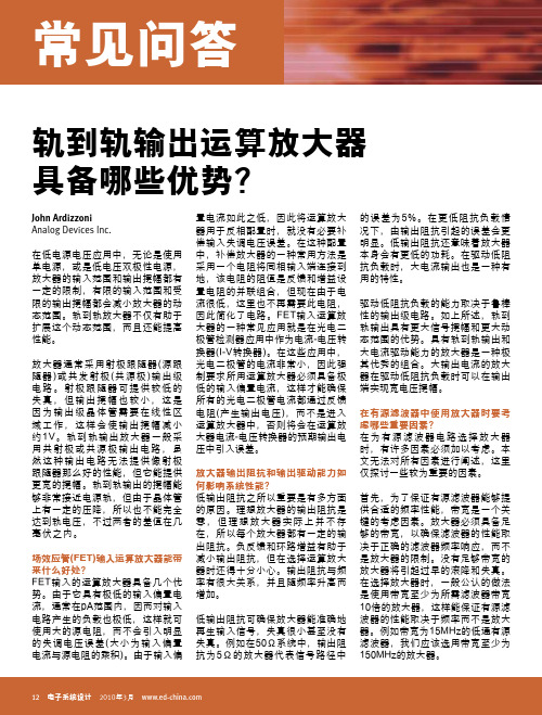
12 20103John Ardizzoni Analog Devices Inc.在低电源电压应用中,无论是使用单电源,或是低电压双极性电源,放大器的输入范围和输出摆幅都有一定的限制,有限的输入范围和受限的输出摆幅都会减小放大器的动态范围。
轨到轨放大器不仅有助于扩展这个动态范围,而且还能提高性能。
放大器通常采用射极跟随器(源跟随器)或共发射极(共源极)输出级电路。
射极跟随器可提供较低的失真,但输出摆幅也较小,这是因为输出级晶体管需要在线性区域工作,这样会使输出摆幅减小约1V。
轨到轨输出放大器一般采用共射极或共源极输出电路,虽然这种输出电路无法提供像射极跟随器那么好的性能,但它能提供更宽的摆幅。
轨到轨输出的摆幅能够非常接近电源轨,但由于晶体管上有一定的压降,所以也不能完全达到轨电压,不过两者的差值在几毫伏之内。
场效应管(FET)输入运算放大器能带来什么好处?FET输入的运算放大器具备几个优势。
由于它具有极低的输入偏置电流,通常在pA范围内,因而对输入电路产生的负载也极低,这样就可使用大的源电阻,而不会引入明显的失调电压误差(大小为输入偏置电流与源电阻的乘积)。
由于输入偏轨到轨输出运算放大器具备哪些优势?置电流如此之低,因此将运算放大器用于反相配置时,就没有必要补偿输入失调电压误差。
在这种配置中,补偿放大器的一种常用方法是采用一个电阻将同相输入端连接到地,该电阻的阻值是反馈和增益设置电阻的并联组合,但现在由于电流很低,这里也不再需要此电阻,因此简化了电路。
FET输入运算放大器的一种常见应用就是在光电二极管检测器应用中作为电流-电压转换器(I-V转换器)。
在这些应用中,光电二极管的电流非常小,因此强制要求所用运算放大器必须具备极低的输入偏置电流,这样才能确保所有的光电二极管电流都通过反馈电阻(产生输出电压),而不是进入运算放大器中,否则将会在运算放大器电流-电压转换器的预期输出电压中引入误差。
放大器输出阻抗和输出驱动能力如何影响系统性能?低输出阻抗之所以重要是有多方面的原因。
轨到轨输出原理 -回复
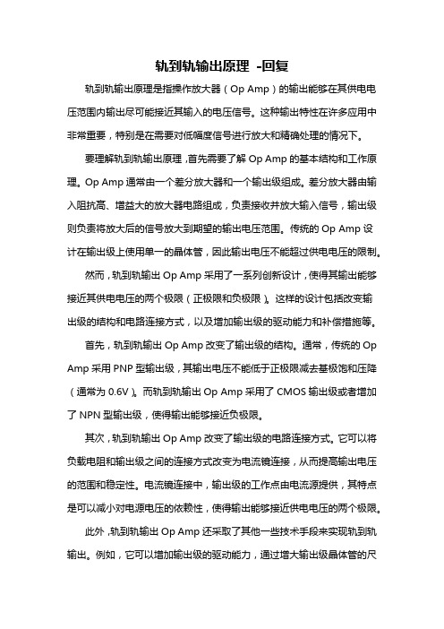
轨到轨输出原理-回复轨到轨输出原理是指操作放大器(Op Amp)的输出能够在其供电电压范围内输出尽可能接近其输入的电压信号。
这种输出特性在许多应用中非常重要,特别是在需要对低幅度信号进行放大和精确处理的情况下。
要理解轨到轨输出原理,首先需要了解Op Amp的基本结构和工作原理。
Op Amp通常由一个差分放大器和一个输出级组成。
差分放大器由输入阻抗高、增益大的放大器电路组成,负责接收并放大输入信号,输出级则负责将放大后的信号放大到期望的输出电压范围。
传统的Op Amp设计在输出级上使用单一的晶体管,因此输出电压不能超过供电电压的限制。
然而,轨到轨输出Op Amp采用了一系列创新设计,使得其输出能够接近其供电电压的两个极限(正极限和负极限)。
这样的设计包括改变输出级的结构和电路连接方式,以及增加输出级的驱动能力和补偿措施等。
首先,轨到轨输出Op Amp改变了输出级的结构。
通常,传统的Op Amp采用PNP型输出级,其输出电压不能低于正极限减去基极饱和压降(通常为0.6V)。
而轨到轨输出Op Amp采用了CMOS输出级或者增加了NPN型输出级,使得输出能够接近负极限。
其次,轨到轨输出Op Amp改变了输出级的电路连接方式。
它可以将负载电阻和输出级之间的连接方式改变为电流镜连接,从而提高输出电压的范围和稳定性。
电流镜连接中,输出级的工作点由电流源提供,其特点是可以减小对电源电压的依赖性,使得输出能够接近供电电压的两个极限。
此外,轨到轨输出Op Amp还采取了其他一些技术手段来实现轨到轨输出。
例如,它可以增加输出级的驱动能力,通过增大输出级晶体管的尺寸或者增加输出级的级数来增加其输出电流能力。
同时,它还可以采用特殊的补偿电路来提高其转换速度和稳定性,以满足各种应用需求。
总的来说,轨到轨输出Op Amp的原理是通过改变输出级的结构和电路连接方式,并增加驱动能力和补偿措施等手段,使得Op Amp的输出能够接近其供电电压的两个极限。
- 1、下载文档前请自行甄别文档内容的完整性,平台不提供额外的编辑、内容补充、找答案等附加服务。
- 2、"仅部分预览"的文档,不可在线预览部分如存在完整性等问题,可反馈申请退款(可完整预览的文档不适用该条件!)。
- 3、如文档侵犯您的权益,请联系客服反馈,我们会尽快为您处理(人工客服工作时间:9:00-18:30)。
MARKING INFORMATION SD06 XXXXX
NOTE: XXXXX = Date Code and Vendor Code.
ABSOLUTE MAXIMUM RATINGS
Supply Voltage, +VS to -VS ................................................. 7.5V Common Mode Input Voltage…..…..(-VS) - 0.5V to (+VS) + 0.5V Storage Temperature Range..............................-65℃ to +150℃ Junction Temperature........................................................160℃ Operating Temperature Range..........................-55℃ to +150℃ Package Thermal Resistance @ TA = +25℃ SOIC-8, θJA....................................................................125℃/W Lead Temperature Range (Soldering 10 sec) ………………………………………..………………………...260℃ ESD Susceptibility HBM..................................................................................1500V MM......................................................................................400V NOTE: Stresses beyond those listed under “Absolute Maximum Ratings” may cause permanent damage to the device. These are stress ratings only, and functional operation of the device at these or any other conditions beyond those indicated in the operational sections of the specifications is not implied. Exposure to absolute maximum rating conditions for extended periods may affect device reliability.
3.5
mV pA pA V
MAX TYP TYP TYP MIN MIN MIN MIN TYP TYP TYP MIN TYP MIN MAX MIN MAX TYP TYP TYP TYP TYP TYP TYP TYP
CAUTION
This integrated circuit can be damaged by ESD if you don’t pay attention to ESD protection. SGMICRO recommends that all integrated circuits be handled with appropriate precautions. Failure to observe proper handling and installation procedures can cause damage. ESD damage can range from subtle performance degradation to complete device failure. Precision integrated circuits may be more susceptible to damage because very small parametric changes could cause the device not to meet its published specifications. SGMICRO reserves the right to make any change in circuit design, specification or other related things if necessary without notice at any time. Please contact SGMICRO sales office to get the latest datasheet.
SG Micro Corp.
2
https://
SD06
(At TA = +25℃, VCM = VS/2, RL = 600Ω, unless otherwise noted.)
470μA, 6MHz, Rail-to-Rail I/O CMOS Operational Amplifier
FEATURES
Low Cost Rail-to-Rail Input and Output
0.8mV Typical VOS
High Gain-Bandwidth Product: 6MHz High Slew Rate: 3.7V/μs Settling Time to 0.1% with 2V Step: 2.1μs Overload Recovery Time: 0.9μs Low Noise: 12nV/
ELECTRICAL CHARACTERISTICS: VS = +5V
SD06 PARAMETER CONDITIONS TYP +25℃ INPUT CHARACTERISTICS Input Offset Voltage (VOS) Input Bias Current (IB) Input Offset Current (IOS) Input Common Mode Voltage Range (VCM) Common Mode Rejection Ratio (CMRR) Open-Loop Voltage Gain (AOL) Input Offset Voltage Drift (ΔVOS/ΔT) OUTPUT CHARACTERISTICS Output Voltage Swing from Rail Output Current (IOUT) Closed-Loop Output Impedance POWER SUPPLY Operating Voltage Range Power Supply Rejection Ratio (PSRR) Quiescent Current/Amplifier (IQ) DYNAMIC PERFORMANCE Gain-Bandwidth Product (GBP) Phase Margin (φO) Full Power Bandwidth (BWP) Slew Rate (SR) Settling Time to 0.1% (tS) Overload Recovery Time NOISE PERFORMANCE Voltage Noise Density (en) Current Noise Density (in) f = 1kHz f = 1kHz 12 3 nV/ fA/
PIN CONFIGURATION (TOP VIEW)
SD06
OUTA 1 -INA 2 +INA 3 -VS 4
SOIC-8
8 7 6 5
+VS OUTB -INB +INB
SG Micro Corp.
September 3, 2012
https://
SD06 470μA, 6MHz, Rail-to-Rail I/O CMOS Operational Amplifier
PRODUCT DESCRIPTION
The SD06 (dual) is a low noise, low voltage, and low power operational amplifier, that can be designed into a wide range of applications. The SD06 has a high gainbandwidth product of 6MHz, a slew rate of 3.7V/μs, and a quiescent current of 470μA/amplifier at 5V. The SD06 is designed to provide optimal performance in low voltage and low noise system. It provides rail-to-rail output swing into heavy load. The input common mode voltage range includes ground, and the maximum input offset voltage is 3.5mV for SD06. It is specified over the extended industrial temperature range (-40℃ to +125℃). The operating range is from 2.5V to 5.5V. The SD06 dual is available in Green SOIC-8 package.
Hz
Supply Voltage Range: 2.5V to 5.5V