SUNLORDINC顺络电子磁珠选型
磁珠叠层电感顺络

叠层
叠层,绕线
滤除噪声,工作在阻抗较大的 频率段,电阻分量占主要因素 。在噪音频段磁珠表现为一个 低Q值的电感,将能量吸收并
以发热形式消耗掉
储能,谐振,匹配,扼流,滤 波。利用了电感的自感储能原
理
阻抗
电感量,SRF,Q值
共同参数
IDC,RDC
IDC,RDC
impedance(Ω) impedance(Ω)
Electromagnetic Susceptibility
(电磁敏感性) 设备、分系统或系 统暴露在电磁辐射 下所呈现的不希望 有的相应程度。
电磁干扰三要素
Sunlord
EXPERT IN PASSIVE PARTS
三要素
干扰源
耦合通道
受感器
传导耦合
辐射耦合
抑制电磁干扰的原理
Sunlord
EXPERT IN PASSIVE PARTS
300
250
200
150
Z
100
R
50
X
0
1
10
100
1000
Frequency(MHz)
Z=R+jX Z2=R2+X2
磁珠的发展趋势
波形失真小
Sunlord
EXPERT IN PASSIVE PARTS
高阻抗
2700Ω 1800Ω 1000Ω
小尺寸
0603 1005 1608
3A 6A 10A
大电流
LC组合电路滤波
消费电子 计算机
共模扼流器
SDCW/SDCWS/-C/-H/-CH/-U
系列
通过发热方式 滤除共模噪声
USB/HDMI/ DVI/IEEE1394
细说磁珠
说说磁珠(Ferrite Bead)第一次使用磁珠还是在实习的时候,但是看原理图发现有个元件写着”Bea d”,单位是100欧姆,用万用表测,导通,电阻约为0。
当时就很奇怪,是什么有什么用?后来问了师兄,才知道,这个是磁珠,相当于电感,通直流阻交流(不准确)。
这就是我当初对磁珠的印象。
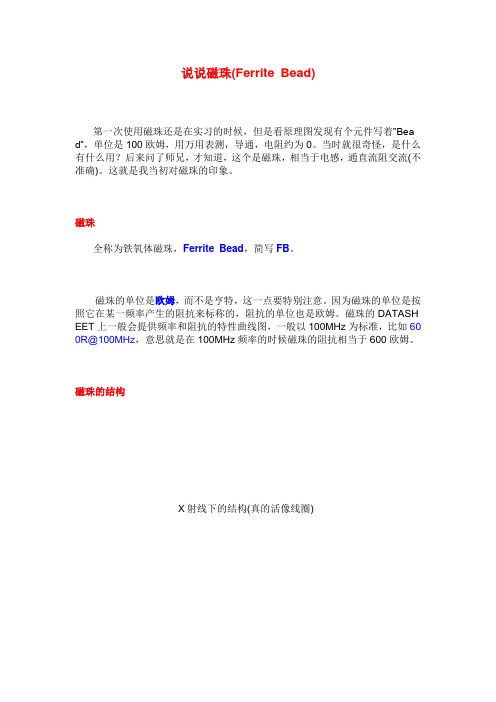
磁珠全称为铁氧体磁珠,Ferrite Bead,简写FB。
磁珠的单位是欧姆,而不是亨特,这一点要特别注意。
因为磁珠的单位是按照它在某一频率产生的阻抗来标称的,阻抗的单位也是欧姆。
磁珠的 DATASH EET上一般会提供频率和阻抗的特性曲线图,一般以100MHz为标准,比如60 0R@100MHz,意思就是在100MHz频率的时候磁珠的阻抗相当于600欧姆。
磁珠的结构X射线下的结构(真的活像线圈)磁珠的等效模型R bead是磁珠的直流电阻;L bead是磁珠的等效电感;Cpar和Rpar是并联电容和电阻。
在低频的时候,Cpar开路,L bead短路,只有直流电阻R bead。
当频率增加的时候,阻抗(JwL bead)随着L bead的增加线性增加,阻抗(1/jwCpar)随着Cpar的减小而相反增长。
磁珠的阻抗频率曲线图上升斜率主要由电感L bead决定。
在高频到达一定频率点时,Cpar的阻抗开始起主要作用。
磁珠的阻抗开始减小。
阻抗频率曲线的斜率下降主要由磁珠的寄生电容Cpar所决定。
Rpar对抑制品质因素(Q-factor)有作用,无论如何,Rpar和Cpar的值增长过大会增加磁珠的品质因素和减小磁珠的有效带宽。
高品质因素(Q)可能导致电源输送网络瞬态频率响应不想要的抬升。
Z=R+jxZ:阻抗R:电阻X:电抗磁珠的电性参数Z(阻抗) [Z]@100MHz (ohm)磁珠的阻抗是指在电流下所有阻抗的总和,包括交流与直流部分。
阻抗的直流部分仅仅是绕线的直流电阻,交流部分包括电感电抗。
下面的公式计算了一个理想电感在正弦交流信号下的电感电抗。
SUNLORDINC顺络电子一级代理分销经销通路供应商KOYUELEC光与电子SDMM0806U

【Version change history】Rev. Effective Date Changed Contents Change reasons Approved By01 / New release / Hai GuoCautionAll products listed in this specification are developed, designed and intended for use in general electronics equipment. The products are not designed or warranted to meet the requirements of the applications listed below, whose performance and/or quality require especially high reliability, or whose failure, malfunction or trouble might directly cause damage to society, person, or property. Please understand that we are not responsible for any damage or liability caused by use of the products in any of the applications below. Please contact us for more details if you intend to use our products in the following applications.1.Aircraft equipment2.Aerospace equipment3.Undersea equipment4.nuclear control equipmentitary equipment6.Power plant equipment7.Medical equipment8.Transportation equipment (automobiles, trains, ships,etc.)9.Traffic signal equipment10.Disaster prevention / crime prevention equipment11.Data-processing equipment12. The application with a long term direct-current voltage difference, which is greater than 1.5V, between D+ and D- of differential lines13. Applications of similar complexity or with reliability requirements comparable to the applications listed in the above1. ScopeThis specification applies to SDMM Series of multi-layer common mode filter. 2.Product Description and Identification (Part Number) 1) DescriptionSDMM Series of multi-layer common mode filter. 2)Product Identification (Part Number) SDMM 0806 U -2 -□□□T ① ② ③ ④ ⑤ ⑥3. Electrical CharacteristicsPlease refer to Appendix A . 1) Operating and storage temperature range (individual chip without packing): -40 ~ +85℃℃ 2) Storage temperature range (packaging conditions): -10~+40 and RH 70% (Max.)℃℃Appendix A: Electrical CharacteristicsPart NumberCommon modeImpedance @ 100MHz(Ω)DC Resistance (Ω) Max.Rated Current (mA) Max.Insulation Resistance (M Ω) Min.Cutoff Frequency(typ.) (GHz) SDMM0806U-2-120T 12±5 2.5 130 100 >8 SDMM0806U-2-350T 35±20% 3.5 100 100 >6SDMM0806U-2-470T 47±20% 4.0 100 100 6 SDMM0806U-2-900T 90±20% 4.51001003.5Note: Absolute maximum long term direct-current voltage between D+ and D- of differential lines: DC 1.5VPacking ⑥TTape Carrier Package① TypeSDMMmultilayer commonmode filter② External Dimensions (L x W) (mm)08060.85×0.65Number of Lines ④-2 2 linesCommon Mode Impedance ⑤ (Ω)Example Nominal Value350 35③Feature TypeUFor Ultra high speedDifferential SignalLinesTypical Electrical CharacteristicsSDMM0806U-2-120T SDMM0806U-2-350TImpedance vs. Frequency(SDMM0806U-2-120T) Impedance vs. Frequency(SDMM0806U-2-350T)Insertion loss vs. Frequency (SDMM0806U-2-120T) Insertion loss vs. Frequency (SDMM0806U-2-350T)Insertion loss vs. Frequency (SDMM0806U-2-120T) Insertion loss vs. Frequency (SDMM0806U-2-350T)SDMM0806U-2-470T SDMM0806U-2-900TImpedance vs. Frequency (SDMM0806U-2-470T) Impedance vs. Frequency (SDMM0806U-2-900T)Insertion loss vs. Frequency (SDMM0806U-2-470T) Insertion loss vs. Frequency (SDMM0806U-2-900T)Insertion loss vs. Frequency (SDMM0806U-2-470T) Insertion loss vs. Frequency (SDMM0806U-2-900T)4. Shape and Dimensions1) Dimensions: See Fig.4-1 and Table 4-1. 2) Equivalent circuit: See Fig. 4-2.3)Recommended PCB pattern for reflow soldering: See Fig. 4-3.4) Structure: See Fig. 4-4 and Fig. 4-5.Material Information: See Table 4-2.[Table 4-2]Code Part NameMaterial Name ① Ceramic Body Ceramic Powder ② Ferrite Body Ferrite Powder ③ Inner Coils(Ag) Silver Paste ④ Pull-out Electrode (Ag) Silver PasteTypeL W T SL SW P 0806 0.85±0.05 0.65±0.05 0.40±0.05 0.20+0.05/-0.10 0.27±0.05 0.50±0.05[Table 4-1] Unit: mmSW(3) (1) (4)(2)(3) (1) (2)(4)For 0806Fig. 4-2Fig. 4-3Fig.4-1①③④⑤Fig. 4-4②①AgStructure of Electro-platingBodyNiSn⑤-1 ⑤-2Fig. 4-55.Test and Measurement Procedures 5.1 Test ConditionsUnless otherwise specified, the standard atmospheric conditions for measurement/test as:a. Ambient Temperature: 20±15℃b. Relative Humidity: 65±20%c.Air Pressure: 86 kPa to 106 kPaIf any doubt on the results, measurements/tests should be made within the following limits:a. Ambient Temperature: 20±2℃b. Relative Humidity: 65±5%c. Air Pressure: 86kPa to 106 kPa 5.2 Visual Examination a. Inspection Equipment: 20× magnifier5.3 Electrical TestItems Requirements Test Methods and Remarks5.3.1 Impedance (Common Mode)Refer to Appendix ATest equipment: High Accuracy RF LCR Meter Agilent4287A/E4991A or equivalent.Common Mode Impedance is tested according to the following circuit.5.3.2 Impedance (Differential Mode)Refer to Appendix ATest equipment: High Accuracy RF LCR Meter Agilent4287A/E4991A or equivalent. Differential Mode Impedance is tested according to the following circuit.5.3.3DC ResistanceRefer to Appendix ATest equipment: High Accuracy Milliohm meter Agilent4338B/34420 or equivalent. DC Resistance is tested according to the following circuit.5.3.4Rated CurrentRefer to Appendix ATest equipment: Electric Power, Electric current meter, Thermometer.Definition of Rated Current (Ir): Ir is direct electric current as chip surface temperature rise just20 against chip initial surface temperature.℃ Rated Current is tested according to the following circuit.5.3.5 Insulation ResistanceRefer to Appendix ATest equipment: High resistance meter Agilent4339B. Withstand Voltage:2.5 times rated voltage Application time:1~5 SecondsThe charging and discharging current::Less than 1mAInsulation Resistance is tested according to the following circuit.5.3.6Insertion LossRefer to Appendix ATest equipment: S-parameter Network Analyzer AgilentE5071C or equivalent. Insertion Loss is S21mag tested according to the following circuit.5.4.10 Loading under damp heat① No visible mechanical damage. ② Impedance change: within ±20%. ③ Insulation Resistance: 100M Ω Min.① Temperature: 60±2.℃ ② Humidity: 90% to 95% RH. ③ Duration: 1000+12hours.④ Applied current: Rated current.⑤ The chip shall be stabilized at normal condition for 1~2 hoursbefore measuring.5.4.11Loading at high temperature (Life test) ① No visible mechanical damage. ② Impedance change: within ±20%. ③ Insulation Resistance: 100M Ω Min.① Temperature: 85±2.℃ ② Duration: 1000+12hours.③ Applied current: Rated current.④The chip shall be stabilized at normal condition for 1~2 hours before measuring.6. Packaging and Storage6.1 PackagingTape Carrier Packaging: Packaging code: T a. Tape carrier packaging are specified in attached figure Fig.6.1-1~4 b.Tape carrier packaging quantity please see the following table:Type 0806 Tape Paper Tape Quantity10Kc. Reel shall be packaged in vinyl bag.d. Maximum of 5 or 10 reels bags shall be packaged in an inner box.e.Maximum of 6 or 10 inner boxes shall be packaged in an outer case.(1)Remark: The sprocket holes are to the right as the tape is pulled toward the user.(2) Taping Dimensions (Unit: mm)Type A B P Tmax 08060.80±0.051.0±0.052.0±0.050.55Chip CavityTSunlord Business categories :Level 0(general confidential ) Specifications for Multi-layer Common Mode Filter Page 11 of 11(3) Reel Dimensions (Unit: mm)6.2 Storage a. The solderability of the external electrode may be deteriorated if packages are stored where they are exposed to high humidity. Package must be stored at 40 or less and 70% RH or less.℃b. The solderability of the external electrode may be deteriorated if packages are stored where they are exposed to dust of harmful gas (e.g. HCl, sulfurous gas of H 2S).c. Packaging material may be deformed if package are stored where they are exposed to heat of direct sunlight.d.Solderability specified in Clause 5.4.6shall be guaranteed for 6 months from the date of delivery on condition that they are stored at the environment specified in Clause 3 .For those parts, which passed more than 6 months shall be checked solder-ability before use.7. Recommended Soldering Technologies7.1 Re-flowing Profile:△ Preheat condition: 150 ~200/60~120℃sec. △ Allowed time above 217: 60~90s ℃ec. △ Max temp: 260℃△ Max time at max temp: 10sec. △ Solder paste: Sn/3.0Ag/0.5Cu △ Allowed Reflow time: 2x max7.2 Iron Soldering Profile.△ Iron soldering power: Max.30W. △ Pre-heating: 150 / 60 sec. ℃ △ Soldering Tip temperature: 350Max.℃ △ Soldering time: 3 sec Max. △ Solder paste: Sn/3.0Ag/0.5Cu. △ Max.1 times for iron soldering. [Note: Take care not to apply the tip of the soldering iron to the terminal electrodes.]CFig.6.1.34.3±0.2mm4.0±0.1mm5.0±0.1mm3.0±0.1mmmax <14.4mm[Note: The reflow profile in the above table is only for qualification and is not meant to specify board assembly profiles. Actual board assembly profiles must be based on the customer's specific board design, solder paste and process, and should not exceed the parameters as the Reflow profile shows.]26015020021725℃ Tc ℃350℃。
细说磁珠
说说磁珠(Ferrite Bead)第一次使用磁珠还是在实习的时候,但是看原理图发现有个元件写着”Bea d”,单位是100欧姆,用万用表测,导通,电阻约为0。
当时就很奇怪,是什么有什么用?后来问了师兄,才知道,这个是磁珠,相当于电感,通直流阻交流(不准确)。
这就是我当初对磁珠的印象。
磁珠全称为铁氧体磁珠,Ferrite Bead,简写FB。
磁珠的单位是欧姆,而不是亨特,这一点要特别注意。
因为磁珠的单位是按照它在某一频率产生的阻抗来标称的,阻抗的单位也是欧姆。
磁珠的 DATASH EET上一般会提供频率和阻抗的特性曲线图,一般以100MHz为标准,比如60 0R@100MHz,意思就是在100MHz频率的时候磁珠的阻抗相当于600欧姆。
磁珠的结构X射线下的结构(真的活像线圈)磁珠的等效模型R bead是磁珠的直流电阻;L bead是磁珠的等效电感;Cpar和Rpar是并联电容和电阻。
在低频的时候,Cpar开路,L bead短路,只有直流电阻R bead。
当频率增加的时候,阻抗(JwL bead)随着L bead的增加线性增加,阻抗(1/jwCpar)随着Cpar的减小而相反增长。
磁珠的阻抗频率曲线图上升斜率主要由电感L bead决定。
在高频到达一定频率点时,Cpar的阻抗开始起主要作用。
磁珠的阻抗开始减小。
阻抗频率曲线的斜率下降主要由磁珠的寄生电容Cpar所决定。
Rpar对抑制品质因素(Q-factor)有作用,无论如何,Rpar和Cpar的值增长过大会增加磁珠的品质因素和减小磁珠的有效带宽。
高品质因素(Q)可能导致电源输送网络瞬态频率响应不想要的抬升。
Z=R+jxZ:阻抗R:电阻X:电抗磁珠的电性参数Z(阻抗) [Z]@100MHz (ohm)磁珠的阻抗是指在电流下所有阻抗的总和,包括交流与直流部分。
阻抗的直流部分仅仅是绕线的直流电阻,交流部分包括电感电抗。
下面的公式计算了一个理想电感在正弦交流信号下的电感电抗。
磁珠选型参数
磁珠选型参数摘要:一、磁珠概述二、磁珠选型参数的重要性三、磁珠选型参数详解1.磁珠材质2.磁珠尺寸3.磁珠磁感应强度4.磁珠电阻5.磁珠频率响应四、选型实战案例分析五、总结与建议正文:一、磁珠概述磁珠,作为一种电子元器件,广泛应用于电子电路中的滤波、耦合、振荡等环节。
它主要由磁性材料制成,具有较高的磁导率和高频阻抗特性。
在众多磁性元器件中,磁珠因其独特的性能而在电子领域占据一席之地。
二、磁珠选型参数的重要性在实际应用中,磁珠的选型至关重要。
一个合适的磁珠不仅能保证电路的正常工作,还能提高整个系统的性能。
因此,了解和掌握磁珠的选型参数显得尤为重要。
三、磁珠选型参数详解1.磁珠材质:磁珠的材质直接影响到其磁性能和稳定性。
常见的磁珠材质有铁氧体(Ferrite)、陶瓷(Ceramic)和金属(Metal)等。
在选型时,需根据实际应用场景选择合适的材质。
2.磁珠尺寸:磁珠的尺寸包括直径、长度和厚度等。
尺寸的选择需结合电路需求和空间限制来确定。
一般来说,磁珠直径越大,容值越大,但体积也越大;长度和厚度的影响则相对较小。
3.磁感应强度:磁感应强度是磁珠的一个重要性能指标,影响着磁珠的磁性能和阻抗特性。
在选型时,需根据电路需求选择合适的磁感应强度。
4.磁珠电阻:磁珠电阻决定了其对交流信号的阻抗特性。
电阻越小,高频性能越好。
但在实际应用中,电阻过小可能导致磁珠发热过多,因此需综合考虑电路需求和散热条件来选择合适的电阻。
5.磁珠频率响应:磁珠的频率响应反映了其在不同频率下的性能表现。
高频响应越好,磁珠对高频信号的抑制能力越强。
在选型时,需根据电路中信号的频率范围选择合适的磁珠。
四、选型实战案例分析以一款手机射频电路为例,需选用一款磁珠来抑制高频干扰。
根据电路需求,可筛选出如下参数:磁珠材质为铁氧体,直径为3mm,长度为10mm,磁感应强度为0.1T,电阻为100Ω,频率响应范围为100kHz~1.7GHz。
五、总结与建议磁珠选型是电子设计中不可或缺的一环。
磁珠的选型和使用
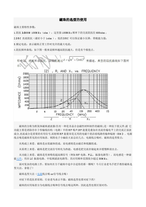
磁珠的选型的使用磁珠主要特性参数:1.阻抗IzI600@100MHz(ohm):这里指100MHz频率下的交流阻抗位600ohm;2.DRC直流阻抗(最好小于1ohm):低的DRC可以保证最小压降,带载能力强;3.额定电流:表示磁珠正常工作时允许的最大电流;4.阻抗频率曲线:如下图一般来说频率越高阻抗越大,但是有个极值点。
磁珠的全称为铁氧体磁珠滤波器(另有一种是非晶合金磁性材料制作的磁珠),是一种抗干扰元件,滤它功能主要是消除存在于传输线结构(电路)中的RF噪声,RF能量是叠加在直流传输电平上的交流正弦波成分,直流成分是需要的有用信号,而射频RF能量却是无用的电磁干扰沿着线路传输和辐射(EMI)。
电源线去噪是磁珠常见的应用场景,硕凯电子小编给大家总结几点,电源线去噪时,磁珠的选型要点:从构成上来看,磁珠是由氧磁体组成,而电感则是由磁芯和线圈组成。
从原理上来看,磁珠是把交流信号转化为热能,电感是把交流存储起来并缓慢释放出去。
从功能上来看,磁珠是用来吸收超高频信号(例如RF电路,PLL,振荡电路等),而电感是一种储能元件,用在LC振荡电路、中低频滤波电路等,其应用频率范围很少超过50MHz。
面对复杂的电路工作,要如何在万千磁珠中选中合适你的那一颗呢?今天行业老鸟手把手教你磁珠选型大法,拿稳了!磁珠选型大法(电源线去噪or信号线去噪)对症下药是医者原则,行业老鸟表示不服:磁珠选型也要对症下药!磁珠的应用场景分为电源线去噪和信号线去噪这两种,因此选型也要区别对待:用于电源线去噪时应注意以下几点第一,你要知道开关电源的工作频率。
一般来讲,电源产生的辐射EMI噪声,通常在小于100MHz-300MHz之间。
因此,选磁珠要选峰值频率小于300MHz低频型的磁珠。
第二,你要知道电源的工作电流。
对于那些放置于开关或非直流信号的磁珠,通常要讲交流信号转换有效值,以此来选择磁珠的额定电流。
额定电流值也是电源线磁珠最大的选择要点。
EMC资料

深圳顺络电子股份有限公司
Sunlord EMC主要解决方法 EMC主要解决方法
I/O Filter Enclosure Shielding Design PCB EMC Design Internal Cable EMC Design
屏蔽 接地 印刷板设计 互连与搭接设计 EMI滤波(滤波器件:电感、磁珠、电容、滤波器等)
辐射耦合
减敏
EMC评定指标 评定指标
CS,CE ,
深圳顺络电子股份有限公司
RS,RE ,
Sunlord 电磁干扰抑制部位
高速信号线上的谐波、辐射噪声 微处理器、视频电路、时钟线、高频模拟电路、振荡器等 直流源处的高频噪声 电源的高频噪声和谐波 I/O接口、其他接口部位的噪声 电缆都是天线,电缆是干扰进出设备的有效途径 PCB布局 数字地与模拟地的去耦
SZ Series PZ Series HZ Series
高频噪声和大电流 HPZ series 线路
47~ 100 ~
500~ 3500 ~
深圳顺络电子股份有限公司
Sunlord
磁珠频谱图及衰减特性图( 磁珠频谱图及衰减特性图(I)
GZ频谱图 频谱图
GZ2012D601
GZ衰减特性图 衰减特性图
功能 滤波吸收元件 滤波模块元件 滤波模块元件 阻抗匹配 滤波模块元件 阻抗匹配
0603(0201) SDCL ~2012(0805)
1nH~470nH
1005(0402) SDHL ~1608(0603)
1nH~180nH
深圳顺络电子股份有限公司
Sunlord 电感的使用频段
产品类型
SDFL SDCL SDHL 使用频率
工频及音频干扰 甚低频干扰 载频干扰
SUNLORDINC顺络电子20200515 CN-Sunlord PPT_已签章

2019年位居全球片式绕线电感产能第三位
深圳市首批科技创新行业龙头企业 电感行业国内第一,处于绝对领先地位
2019年“中国电子元件百强企业” 排名27位
片式电感产品全球市场份额超过10%
Page 7 of 26
财务总监 徐佳
总工程师 郭海
汽车电子副总裁 李家凯
副总裁 高海明
绕线产品 厂房 D
叠层产品 厂房 A
LTCC 技术产品 厂房 B
天线产品 厂房 C
Page 4 of 26
贵阳工厂
位置: 贵州省贵阳 厂房面积: 38,000 ㎡ 员工人数: 711人(2019年12月) 获得证书: ISO9001/GJB9001 产 品 线: 片式绕线电感、 功率电感、变压器
东莞工厂2(建设中)
小型化
大电流
模块
LTCC产品
车规级
Page 20 of 26
CNAS认可实验室 符合ISO/ IEC17025:2005 要求
符合UL认证实验室
“顺络-是德”电子测量联 合实验室
材料分析
扫描电镜, X-射线荧光光谱测量机, 热重分析仪, 等等
失效分析
抛光研磨机, X-Ray CT仪, 探针台, 等等
Page 12 of 26
氧化锆陶瓷产品
手机背板、智能穿戴壳体、指纹识别盖片
PDS 天线
NFC 产品
磁性片、柔性天线
PCB
4~8层通孔&二阶HDI板
Page 13 of 26
6
7
8
1
3 4 5
1 LED灯 2 电池管理系统 3 信息娱乐系统 4 驾驶辅助系统 2 5 T-BOX 6 车载充电 7 DC/DC 转换 8 电机驱动