C8051F02X外部存储器接口和IO端口配置
基于C8051F02x单片机外部存储器的设计

o hp 。所谓 混 合 信 号 是 指 单 片 机 的引 脚 既 nC i)
有模 拟 信号 , 又有数 字信 号 。有 些 芯片 的引脚通 过 配 置既 可 以用 于模 拟信号 接 口, 可以用 于数字 信 也
号 接 口。这种具 有 混 合 信号 的功 能 为用 户设 计各 种各 样 的嵌入式 产 品带来 了更 多 的灵 活性 和 多样 性, 而系 统级芯 片 S C则 是 指 将计 算 机 的 硬 、 o 软件
2 C 0 1 0 x单 片 机 的存 储 器 结 构 85 F2
C 0 1O x沿 袭 了 8 5 85F2 0 1单 片 机 的存 储 结 构 。 芯片 内已集 成 了 6 k字节 F A H存储 器 , 4 LS 即程序存
基 于 C 0 1 0 x单 片 机 外 部 存 储 器 的 设 计 85 2 F
刘 志 京
( 京 印刷 学 院 ,北 京 1 2 0 ) 北 06 0
摘
要 :介 绍 了 C 0 1 0 x单 片机 及 其 存 储 结 构 , 其 数 85 F 2 就
据 扩 展 和 接 口功 能进 行 了分 析 , 阐述 了外 部 数 据 存 储 器 的 结 构 和 扩 展 的技 术 要 求 。 在 访 问或 扩 展 外 部 数 据 存 储 器 的 过 程 中, 过 外 部 存 储 器 接 口( MI ) 使 其 数据 存 储 器 通 E F ,
数据采 集 和 控 制 系 统 中常 用 的模 拟 和 数 字 外 设 、 6 k字节 F A H存 储器 和 位 于核 外 部数 据 存储 器 4 LS 空间 的 4 B A 即 X A k R M( R M) 内部 振荡器 和复 位 电 、
路 以及 其 他 功 能 部 件 等 。 这 种 系 统 级 芯 片 的 高
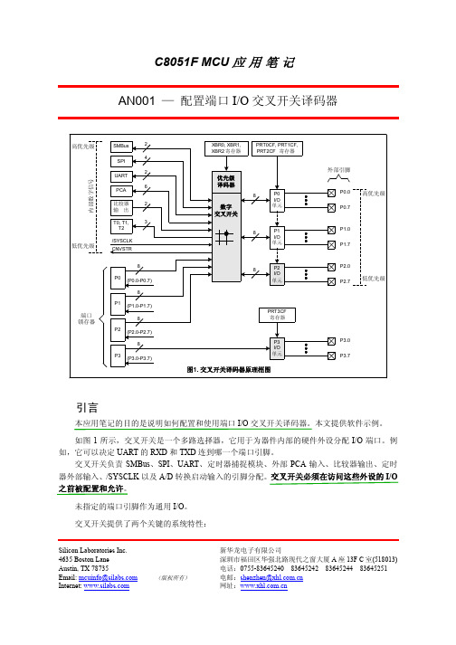
C8051F系列配置端口IO交叉开关译码器
2
AN01-1.1
AN001 — 配置端口 I/O 交叉开关译码器
引脚 P0.4。所有未分配的引脚作为通用 I/O。
例1
假设一个应用需要:
SPI
UART 两个捕捉模块
/INT0 T2。 参考图 2-图 4 中的 I/O 端口交叉开关寄存器说明,交叉开关寄存器配置如下: XBR0=00010110b;允许 UART、两个捕捉模块和 SPI XBR1=00100100b;允许 T2 和/INT0 XBR2=01000000b;允许交叉开关 从表 4 的顶部开始我们发现 SPI 引脚将占用 P0.[0..3](因为不使用 SMBus),UART 占用引脚 P0.[4..5],CEX0 占用 P0.6,CEX1 占用 P0.7,/INT0 占用 P1.0,T2 占用 P1.1。其它端口引脚 P1.[2..7] 和 P2.[0..7]作为通用端口引脚。引脚分配情况列于表 1。
C8051F MCU 应 用 笔 记 AN001 — 配置端口 I/O 交叉开关译码器
高优先级
低优先级 端口 锁存器
内部数字信号
SMBus
2
4 SPI
2 UART
6 PCA
比较器
2
输出
T0, T1,
3
T2
/SYSCLK CNVSTR
8 P0 (P0.0-P0.7)
8 P1 (P1.0-P1.7)
8 P2 (P2.0-P2.7)
未指定的端口引脚作为通用 I/O。
交叉开关提供了两个关键的系统特性:
Silicon Laboratories Inc. 4635 Boston Lane Austin, TX 78735 Email: mcuinfo@ Internet:
c8051f单片机教程
内容:西安科技大学科技创新实验班C8051F单片机教程之一作者:苗瑞日期:2009-12-8网站:/bbs一、认识C8051F并与51比较本节主要是让初学C8051F单片机的学员有个感性的认识,着重强调理论方面的知识,并通过与51单片机的比较,让大家能有更深刻的体会。
1、C8051F单片机简介C8051Fxxx 系列单片机是完全集成的混合信号系统级芯片,具有与8051 兼容的微控制器内核,与MCS-51 指令集完全兼容。
除了具有标准8052 的数字外设部件之外,片内还集成了数据采集和控制系统中常用的模拟部件和其它数字外设及功能部件MCU 中的外设或功能部件包括模拟多路选择器、可编程增益放大器、ADC、DAC、电压比较器、电压基准、温度传感器、SMBus/ I2C、UART、SPI、可编程计数器/定时器阵列(PCA)、定时器、数字I/O 端口、电源监视器、看门狗定时器(WDT)和时钟振荡器等。
所有器件都有内置的FLASH 程序存储器和256 字节的内部RAM,有些器件内部还有位于外部数据存储器空间的RAM,即XRAM。
C8051Fxxx 单片机采用流水线结构,机器周期由标准的12 个系统时钟周期降为1 个系统时钟周期,处理能力大大提高,峰值性能可达25MIPS。
C8051Fxxx 单片机是真正能独立工作的片上系统(SOC)。
每个MCU 都能有效地管理模拟和数字外设,可以关闭单个或全部外设以节省功耗。
FLASH 存储器还具有在系统重新编程能力,可用于非易失性数据存储,并允许现场更新8051 固件。
应用程序可以使用MOVC 和MOVX 指令对FLASH 进行读或改写,每次读或写一个字节。
这一特性允许将程序存储器用于非易失性数据存储以及在软件控制下更新程序代码。
片内 JTAG 调试支持功能允许使用安装在最终应用系统上的产品MCU 进行非侵入式(不占用片内资源)、全速、在系统调试。
该调试系统支持观察和修改存储器和寄存器,支持断点、单步、运行和停机命令。
C8051F02X外部存储器接口和IO端口配置

C8051F02X外部存储器接口和IO端口配置美国Cygnal公司C8051F02X系列单片机是集成在一起芯片上的混合信号系统级单片机。
该单片机具有32/64位数字I/O端口(引脚)、25MIPS高速流水线式8051微控制器内核、64KB在系统可编程Flash存储器、64KB地址的外部存储器接口、4352(4096256)B 片内RAM、各自*的SPI、SMBUS/I2C和两个UART串行接口等特点。
其最突出的优点就是,通过设置交叉开关寄存器控制片内数字资源映*到外部I/O引脚,这就允许用户根据自己的特定应用,选择通用I/O端口和所需要数字资源。
当然,在设置数字交叉开关寄存器时,应该首先考虑EMIF的配置问题。
其配置不同,将导致单片机通过不同的端口(低或高)访问片外存储器和存储器映像的I/O部件,以及数字交叉开关是否分配外部设备给P0.7(WR)、P0.6(RD)、P0.5(ALE)引脚。
(如图EMIF设置为多路器模式。
)1EMIF和I/O配置方法1.1外部存储器接口(EMIF)配置C8051F02X系列MCU有4KB的RAM可以只映*在片内,也可以映*在64KB外部数据存储器地址空间,还可以同时映*到片内和片外(4KB地址以内在片内存储器空间访问,4KB以上经过EMIF访问)三种方式。
对于后两种存储器工作模式,需通过外部存储器接口使用MOVX和DPTR或MOVX和R0(R1)指令访问外部数据存储器和存储器映像的I/O设备。
但是对于高8位地址,必须由外部存储器接口寄存器(EMI0CN)提供;而EMIF可将外部数据存储器接口映*到低端口(P0~P3)(F020/2/3系列)或高端口(P4~P7)(F020/2系列),以及配置为复用模式或非复用模式等。
配置外部存储器接口的步骤下:*设置EMIF为低端口或高端口;*设置EMIF为复用模式或非复用模式;*选择存储器模式(片内方式、无块选择分片方式、带块选择分片方式、片外方式);*设置片外存储器或片外设备时基;*选择相关I/O端口(寄存器PnMOUT、P74OUT)的输出模式。
C8051F020学习笔记-IO初始化

二,使用过程中,常常出现程序的IO口设置,包括设置为交叉开关,推挽方式等。
由于对这种设置方法不太了解,因此做一个专题。
//--------------------------------------------------------------------// I/O初始化程序//--------------------------------------------------------------------// 配置交叉开关和 GPIO 端口void xbar_init (void){XBR0 = 0x07; // 允许 I2C SPI和 UARTXBR1 = 0x00; //XBR2 = 0x40; // 允许交叉开关和弱上拉//PRT0CF |= 0xff; // 允许P0口的所有输出为弱上拉//P0MDOUT// 让交叉开关将这些引脚配置为输入//PRT1CF |= 0x40; // 允许 P1.6 (LED) 为弱上拉输出}(通过对比几个程序的I/O初始化,发现主要是对寄存器XBR0~2以及PRT(0~7)CF进行设置。
特将与IO口设置相关的寄存器做一个说明)2.1 GPIO口和数字外设口C8051F020/1/2/3 MCU 是高集成度的混合信号片上系统,有按8 位端口组织的64 个数字I/O 引脚。
低端口(P0、P1、P2 和P3)既可以按位寻址也可以按字节寻址。
高端口(P4、P5、P6 和P7)只能按字节寻址。
所有引脚都耐5V 电压,都可以被配置为漏极开路或推挽输出方式和弱上拉。
C8051F020/1/2/3 器件有大量的数字资源需要通过4 个低端I/O 端口P0、P1、P2 和P3 才能使用。
P0、P1、P2 和P3 中的每个引脚既可定义为通用的端口I/O(GPIO)引脚,又可以分配给一个数字外设或功能(例如:UART0 或/INT1),这种资源分配的灵活性是通过使用优先权交叉开关译码器实现的。
C8051F2xx 开发板用户指南说明书
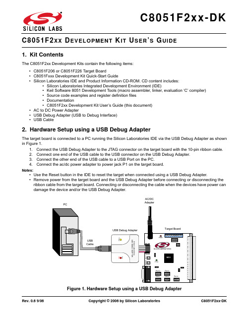
Rev. 0.6 9/06Copyright © 2006 by Silicon LaboratoriesC8051F2xx-DKXX EVELOPMENT IT SER S UIDE1. Kit ContentsThe C8051F2xx Development Kits contain the following items:•C8051F206 or C8051F226 Target Board•C8051Fxxx Development Kit Quick-Start Guide•Silicon Laboratories IDE and Product Information CD-ROM. CD content includes:•Silicon Laboratories Integrated Development Environment (IDE)•Keil Software 8051 Development Tools (macro assembler, linker, evaluation ‘C’ compiler)•Source code examples and register definition files •Documentation•C8051F2xx Development Kit User’s Guide (this document)•AC to DC Power Adapter•USB Debug Adapter (USB to Debug Interface)•USB Cable2. Hardware Setup using a USB Debug AdapterThe target board is connected to a PC running the Silicon Laboratories IDE via the USB Debug Adapter as shown in Figure 1.1.Connect the USB Debug Adapter to the JTAG connector on the target board with the 10-pin ribbon cable.2.Connect one end of the USB cable to the USB connector on the USB Debug Adapter.3.Connect the other end of the USB cable to a USB Port on the PC.4.Connect the ac/dc power adapter to power jack P1 on the target board.Notes:•Use the Reset button in the IDE to reset the target when connected using a USB Debug Adapter.•Remove power from the target board and the USB Debug Adapter before connecting or disconnecting the ribbon cable from the target board. Connecting or disconnecting the cable when the devices have power can damage the device and/or the USB Debug Adapter.Figure 1. Hardware Setup using a USB Debug AdapterPWRP1.6C8051F2xx-DK3. Software SetupThe included CD-ROM contains the Silicon Laboratories Integrated Development Environment (IDE), Keil software 8051 tools and additional documentation. Insert the CD-ROM into your PC’s CD-ROM drive. An installer will auto-matically launch, allowing you to install the IDE software or read documentation by clicking buttons on the Installa-tion Panel. If the installer does not automatically start when you insert the CD-ROM, run autorun.exe found in the root directory of the CD-ROM. Refer to the readme.txt file on the CD-ROM for the latest information regarding known IDE problems and restrictions.4. Silicon Laboratories Integrated Development EnvironmentThe Silicon Laboratories IDE integrates a source-code editor, source-level debugger and in-system Flash program-mer. The use of third-party compilers and assemblers is also supported. This development kit includes the Keil Software A51 macro assembler, BL51 linker and evaluation version C51 ‘C’ compiler. These tools can be used from within the Silicon Laboratories IDE.4.1. System RequirementsThe Silicon Laboratories IDE requirements:•Pentium-class host PC running Microsoft Windows 98SE or later.•One available COM or USB port.•64 MB RAM and 40MB free HD space recommended.4.2. Assembler and LinkerA full-version Keil A51 macro assembler and BL51 banking linker are included with the development kit and are installed during IDE installation. The complete assembler and linker reference manual can be found under the Help menu in the IDE or in the “SiLabs\MCU\hlp” directory (A51.pdf).4.3. Evaluation C51 ‘C’ CompilerAn evaluation version of the Keil C51 ‘C’ compiler is included with the development kit and is installed during IDE installation. The evaluation version of the C51 compiler is the same as the full professional version except code size is limited to 4kB and the floating point library is not included. The C51 compiler reference manual can be found under the Help menu in the IDE or in the “SiLabs\MCU\hlp” directory (C51.pdf).4.4. Using the Keil Software 8051 Tools with the Silicon Laboratories IDETo perform source-level debugging with the IDE, you must configure the Keil 8051 tools to generate an absolute object file in the OMF-51 format with object extensions and debug records enabled. You may build the OMF-51 absolute object file by calling the Keil 8051 tools at the command line (e.g. batch file or make file) or by using the project manager built into the IDE. The default configuration when using the Silicon Laboratories IDE project manager enables object extension and debug record generation. Refer to Applications Note AN104 - Integrating Keil 8051 Tools Into the Silicon Labs IDE in the “SiLabs\MCU\Documentation\Appnotes” directory on the CD-ROM for additional information on using the Keil 8051 tools with the Silicon Laboratories IDE.To build an absolute object file using the Silicon Laboratories IDE project manager, you must first create a project.A project consists of a set of files, IDE configuration, debug views, and a target build configuration (list of files and tool configurations used as input to the assembler, compiler, and linker when building an output object file).The following sections illustrate the steps necessary to manually create a project with one or more source files, build a program and download the program to the target in preparation for debugging. (The IDE will automatically create a single-file project using the currently open and active source file if you select Build/Make Project before a project is defined.)C8051F2xx-DK4.4.1. Creating a New Project1.Select Project→New Project to open a new project and reset all configuration settings to default.2.Select File→New File to open an editor window. Create your source file(s) and save the file(s) with a rec-ognized extension, such as .c, .h, or .asm, to enable color syntax highlighting.3.Right-click on “New Project” in the Project Window. Select Add files to project. Select files in the filebrowser and click Open. Continue adding files until all project files have been added.4.For each of the files in the Project Window that you want assembled, compiled and linked into the targetbuild, right-click on the file name and select Add file to build. Each file will be assembled or compiled as appropriate (based on file extension) and linked into the build of the absolute object file.Note: If a project contains a large number of files, the “Group” feature of the IDE can be used to organize.Right-click on “New Project” in the Project Window. Select Add Groups to project. Add pre-definedgroups or add customized groups. Right-click on the group name and choose Add file to group. Select files to be added. Continue adding files until all project files have been added.4.4.2. Building and Downloading the Program for Debugging1.Once all source files have been added to the target build, build the project by clicking on the Build/MakeProject button in the toolbar or selecting Project→Build/Make Project from the menu.Note: After the project has been built the first time, the Build/Make Project command will only build the files that have been changed since the previous build. To rebuild all files and project dependencies, click on the Rebuild All button in the toolbar or select Project→Rebuild All from the menu.2.Before connecting to the target device, several connection options may need to be set. Open theConnection Options window by selecting Options→Connection Options... in the IDE menu. First, select the appropriate adapter in the “Serial Adapter” section. Next, the correct “Debug Interface” must be selected.C8051F2xx family devices use the JTAG debug interface. Once all the selections are made, click the OK button to close the window.3.Click the Connect button in the toolbar or select Debug→Connect from the menu to connect to the device.4.Download the project to the target by clicking the Download Code button in the toolbar.Note: To enable automatic downloading if the program build is successful select Enable automatic con-nect/download after build in the Project→Target Build Configuration dialog. If errors occur during the build process, the IDE will not attempt the download.5.Save the project when finished with the debug session to preserve the current target build configuration,editor settings and the location of all open debug views. To save the project, select Project->Save Project As... from the menu. Create a new name for the project and click on Save.C8051F2xx-DK5. Example Source CodeExample source code and register definition files are provided in the “SiLabs\MCU\Examples\C8051F2xx”directory during IDE installation. These files may be used as a template for code development. Example applications include a blinking LED example which configures the green LED on the target board to blink at a fixed rate.5.1. Register Definition FilesRegister definition files C8051F200.inc and C8051F200.h define all SFR registers and bit-addressable control/status bits. They are installed into the “SiLabs\MCU\Examples\C8051F2xx” directory during IDE installation. The register and bit names are identical to those used in the C8051F2xx data sheet. Both register definition files are also installed in the default search path used by the Keil Software 8051 tools. Therefore, when using the Keil 8051 tools included with the development kit (A51, C51), it is not necessary to copy a register definition file to each project’s file directory.5.2. Blinking LED ExampleThe example source files blink.asm and blinky.c show examples of several basic C8051F2xx functions. These include; disabling the watchdog timer (WDT), configuring the Port I/O crossbar, configuring a timer for an interrupt routine, initializing the system clock, and configuring a GPIO port. When compiled/assembled and linked this program flashes the green LED on the target board about five times a second using the interrupt handler with a timer.C8051F2xx-DK 6. Target BoardThe C8051F2xx Development Kit includes a target board with a C8051F206/26 device pre-installed for evaluation and preliminary software development. Numerous input/output (I/O) connections are provided to facilitate prototyping using the target board. Refer to Figure2 for the locations of the various I/O connectors.P1Power connector (accepts input from 7 to 15 VDC unregulated power adapter)J1VDDMonEn, Ties MONEN to +3VD2 or GND to enable/disable the VDD monitorJ264-pin I/O connector providing access to all I/O signalsP2.5Connects SW2 to port pin P2.5LED Connects LED D2 to port pin P2.4PWMIN Connects PWM low-pass filter to port pin P2.7J4JTAG connector for Debug Adapter interfaceJ5Connects P3.0 to analog signal from J6J6Analog I/O configuration connectorJ7Connects P3.1 to analog signal from J6X1Analog I/O terminal blockFigure 2. C8051F206 and C8051F226 Target BoardsC8051F2xx-DK6.1. System Clock SourcesThe C8051F2xx device installed on the target board features a internal oscillator which is enabled as the system clock source on reset. After reset, the internal oscillator operates at a frequency of 2MHz (+/-2%) by default but may be configured by software to operate at other frequencies. Therefore, in many applications an external oscillator is not required. However, an external crystal may be installed on the target board for additional applications. The target board is designed to facilitate the installation of an external crystal at the pads marked Q1. Refer to the C8051F2xx datasheet for more information on configuring the system clock source. Following are a few part numbers of suitable crystals:Freq(MHz)Digikey P/N ECS P/N22.1184X063-ND ECS-221-20-1 (20pF loading capacitance)18.432X146-ND ECS-184-20-1 (20pF loading capacitance)11.0592X089-ND ECS-110.5-20-1 (20pF loading capacitance)6.2. Switches and LEDsTwo switches are provided on the target board. Switch SW1 is connected to the RESET pin of the C8051F2xx device on the target board. Pressing SW1 puts the device into its hardware-reset state. The device will leave the reset state after SW1 is released. Switch SW2 is connected to the device’s general purpose I/O (GPIO) pin through headers. Pressing SW2 generates a logic low signal on the port pin. Remove the shorting block from the header to disconnect SW2 from the port pins. The port pin signal is also routed to a pin on the J2 I/O connector. See Table1 for the port pins and headers corresponding to each switch.Two LEDs are also provided on the target board. The red LED labeled PWR is used to indicate a power connection to the target board. The green LED labeled with a port pin name is connected to the device’s GPIO pin through headers. Remove the shorting block from the header to disconnect the LED from the port pin. The port pin signal is also routed to a pin on the J2 I/O connector. See Table1 for the port pins and headers corresponding to each LED.Table 1. Target Board I/O DescriptionsDescription I/O HeaderSW1Reset noneSW2P2.5P2.5Green LED P2.4LEDRed LED PWR none6.3. Target Board JTAG Interface (J4)The JTAG connector (J4) provides access to the JTAG pins of the C8051F2xx. It is used to connect the Serial Adapter or the USB Debug Adapter to the target board for in-circuit debugging and Flash programming. Table2 shows the JTAG pin definitions.Table 2. JTAG Connector Pin DescriptionsPin #Description1+3VD (+3.3VDC)2, 3, 9GND (Ground)4TCK5TMS6TDO7TDI8, 10Not ConnectedC8051F2xx-DK6.4. Analog I/O (J5, J6, J7, Terminal Block)An Analog I/O Configuration connector (J6) provides the ability to route analog I/O signals from the C8051F2xx to a terminal block in addition to connector J2 by installing shorting blocks on J6. Additionally, if shorting blocks are installed on J5 and J7, the analog signals routed through J6 can be inputs to the C8051F2xx at port pins P3.0 and/or P3.1. The port pins can then be configured as inputs to the on-chip ADC for evaluation. J6 also allows the user to route analog signals from the terminal block to port pins P1.3 and P1.4. These port pin can then be configured as inputs to Comparator 1. The PWM signal from the low-pass filter is also routed to J6 to provide a user controlled analog voltage level. This signal can then be used to evaluate the on-chip ADC by placing a shorting block on J6 (provided the J5 or J7 header is shorted). Refer to Figure3 to determine the shorting block installation positions required to create the desired analog signal paths. Refer to Table3 for terminal block connections and Table4 for J6 pin definitions.Figure 3. J6 Analog I/O Configuration ConnectorTable 3. Terminal Block Pin DescriptionsPin #Description1VREF2GND7AIN28AIN1Table 4. J6 Connector Pin DescriptionsPin #Description1P1.4/CP1-2, 9, 10NC3AIN24P3.0AIN5P1.3/CP1+6PWM7AIN18P3.1AIN6.5. VDD Monitor Disable (J1)The VDD Monitor of the C8051F2xx may be disabled by moving the shorting block on J1 from pins 1-2 to pins 2-3, as shown in Figure4.Figure 4. VDD Monitor Hardware SetupC8051F2xx-DK6.6. Low-pass Filter (PWMIN)The C8051F2xx target board features a low-pass filter that may be connected to port pin P2.7. Install a shorting block on connector “PWMIN” to connect the P2.7 pin of the target device to the low-pass filter input. The output of the low-pass filter is routed to the PWM signal at J6[6]. To route the PWM signal to the ADC on the target device, a shorting block should be placed on “PWMIN”, and a shorting block placed on connector “P3.0AIN” (J5) or “P3.1AIN” (J7). Connector J6 is used to connect the PWM voltage to the P3.0AIN or P3.1AIN signal routed to the corresponding port pins (See Figure3). These port pins are then configured for use by the ADC.The C8051F2xx may be programmed to generate a PWM (Pulse-Width Modulated) waveform which is then input to the low-pass filter to implement a user-controlled PWM digital-to-analog converter. Refer to Applications Note AN110 - Implementing 16-Bit PWM Using an On-Chip Timer in the “Documentation” directory on the CD-ROM for a discussion on generating a programmable dc voltage level with a PWM waveform and low-pass filter.6.7. Expansion I/O Connector (J2)The target board provides access to all C8051F2xx signals (except the four JTAG signals: TCK, TMS, TDO and TDI used to connect the Emulation Cartridge – these are accessed using test points in place near the J4 header) via the 64-pin connector J2. A small through-hole prototyping area is also provided. All I/O signals routed to connector J2 are also routed to through-hole connection points between J2 and the prototyping area (see Figure2). The signal layout pattern of these connection points is identical to the adjacent J2 connector pins. Table5 shows the pin-out of the J2 connector.Table 5. J2 Pin DescriptionsPin Description Pin Description1,46,64+3VD2 (voltage supply)21P2.42XTAL122P2.53P1.623P2.24P1.724P2.35P1.425P2.06P1.526P2.17P1.227P3.68P1.328P3.79P1.029P3.410P1.130P3.511P0.631P3.212P0.732P3.313P0.433P3.014P0.534P3.115P0.236/RST16P0.339,41,42,45,47,63GND17P0.048,50PWM (pulse-width modulator) 18P0.153VREF19P2.662VDDMONEN20P2.7C8051F2xx-DK 7. SchematicC8051F2xx-DKD OCUMENT C HANGE L ISTRevision 0.4 to Revision 0.5⏹Section 1, added USB Debug Adapter and USB Cable.⏹Section 2, changed name from "Hardware Setup" to "Hardware Setup using an EC2 Serial Adapter".⏹Section 2, added 2 Notes bullets.⏹Section 2, removed Note from bottom of page.⏹Added Section 3, "Hardware Setup using a USB Debug Adapter".⏹Section 5.4.2, changed step 2 to include new instructions.⏹Section 7, J4, changed "Serial Adapter" to "Debug Adapter".⏹Target Board DEBUG Interface Section, added USB Debug Adapter.⏹DEBUG Connector Pin Descriptions Table, changed pin 4 to C2D.⏹Changed "jumper" to "header".⏹EC2 Serial Adapter section, added EC2 to the section title, table title and figure title.⏹EC2 Serial Adapter section, changed "JTAG" to "DEBUG".⏹Added "USB Debug Adapter" section.Revision 0.5 to Revision 0.6⏹Removed EC2 Serial Adapter from Kit Contents.⏹Removed Section 2. Hardware Setup using an EC2 Serial Adapter. See RS232 Serial Adapter (EC2) User's Guide.⏹Removed Section 8. EC2 Serial Adapter. See RS232 Serial Adapter (EC2) User's Guide.⏹Removed Section 9. USB Debug Adapter. See USB Debug Adapter User's Guide.DisclaimerSilicon Laboratories intends to provide customers with the latest, accurate, and in-depth documentation of all peripherals and modules available for system and software implementers using or intending to use the Silicon Laboratories products. Characterization data, available modules and peripherals, memory sizes and memory addresses refer to each specific device, and "Typical" parameters provided can and do vary in different applications. Application examples described herein are for illustrative purposes only. Silicon Laboratories reserves the right to make changes without further notice and limitation to product information, specifications, and descriptions herein, and does not give warranties as to the accuracy or completeness of the included information. Silicon Laboratories shall have no liability for the consequences of use of the information supplied herein. This document does not imply or express copyright licenses granted hereunder to design or fabricate any integrated circuits. The products must not be used within any Life Support System without the specific written consent of Silicon Laboratories. A "Life Support System" is any product or system intended to support or sustain life and/or health, which, if it fails, can be reasonably expected to result in significant personal injury or death. Silicon Laboratories products are generally not intended for military applications. Silicon Laboratories products shall under no circumstances be used in weapons of mass destruction including (but not limited to) nuclear, biological or chemical weapons, or missiles capable of delivering such weapons.Trademark InformationSilicon Laboratories Inc., Silicon Laboratories, Silicon Labs, SiLabs and the Silicon Labs logo, CMEMS®, EFM, EFM32, EFR, Energy Micro, Energy Micro logo and combinations thereof, "the world’s most energy friendly microcontrollers", Ember®, EZLink®, EZMac®, EZRadio®, EZRadioPRO®, DSPLL®, ISOmodem ®, Precision32®, ProSLIC®, SiPHY®, USBXpress® and others are trademarks or registered trademarks of Silicon Laboratories Inc. ARM, CORTEX, Cortex-M3 and THUMB are trademarks or registered trademarks of ARM Holdings. Keil is a registered trademark of ARM Limited. All other products or brand names mentioned herein are trademarks of their respective holders. Silicon Laboratories Inc.400 West Cesar ChavezAustin, TX 78701USAIoT Portfolio/IoT SW/HW /simplicity Quality /quality Support and Community 。
C8051F单片机的IO口设置

C8051F单片机的IO口设置c8051f020 I/O配置小结2007-04-06 23:05020的每个I/O口引脚都可以被配置为推挽或漏极开路输出。
同时引入了数字交叉开关,允许将内部数字系统资源映射到P0、P1、P2和P3的端口引脚。
通过设置交叉开关寄存器可将片内的计数器/定时器、串行总线、硬件中断、ADC转换启动输入、比较器输出以及微控制器内部的其他数字信号配置为出现在端口I/O引脚。
必须在访问这些外设的I/O之前配置和允许交叉开关。
注意的问题:1.低端口既能按位寻址,也可以按字节寻址;高端口只能按字节寻址。
2.没有被分配到的引脚作为一般的数字通用I/O口。
3.P1口还可以用作ADC1的模拟输入。
4.P0MDOUT~P3MDOUT用于控制I/O端口每一位的输出状态。
5.EMIF(外部存储器接口)是用于CPU与片外XRAM之间的数据传输通道,通过寄存器EMI0CF和EMI0CN选择和管理端口实现数据的传输。
6.为了能访问片外存储器空间,必须设置EMI0CN寄存器的内容为片外存储器的空间页地址。
7.如果把外部存储器接口(EMIF)设置在高端口则首先要把EMI0CF的PRTSEL位设置为1,选择高端口,同时选择地址的复用或非复用方式,在把XBR的外部寄存器的EMIFLE位设置为0。
8.复用方式配置:在复用方式下,数据总线和地址总线的第8位共用相同的引脚(AD0~AD7)。
在该方式下,要用一个外部锁存器(如74HC373或相同功能的锁存器)保持RAM地址的低8位。
外部锁存器由ALE(地址锁存使能)信号控制,ALE 信号由外部存储器接口逻辑驱动。
9.在总线复用时,需要把地址数据复用端口配置为漏极开路。
10.ALE高/低脉宽占1个SYSCLK周期,地址建立/保持时间占0个SYSCLK周期,/WR和/RD占12个SYSCLK周期,EMIF工作在地址/数据复用方式,即:EMI0CF |= 0x2c;EMI0TC |= 0x2c;配置EMIF的步骤是:先将EMIF选到低端口或高端口;然后选择复用方式或非复用方式;再选择存储器的模式(只用片内存储器、不带块选择的分片方式、带块选择的分片方式或只用片外存储器);然后设置EMI0TC;最后通过寄存器PnMDOUT和P74OUT选择所期望的相关端口的输出方式。
C8051F020入门指导

DAC为电压输出方式,有灵活的输出更新机制。这一机制允许
用软件写和定时器2、定时器3及定时器4的溢出信号更新DAC输出。
C8051F020/2的DAC之电压基准由专用的VREFD输入引脚提供,而
C8051F021/3的DAC之电压基准由器件内部的电压基准提供。DAC在
作为比较器的参考电压或为ADC差分输入提供偏移电压时非常有用。
➢
真正8 位500 ksps 的ADC,带PGA 和8 通道模拟多路开关
➢
两个12 位DAC,具有可编程数据更新方式
➢
64K 字节可在系统编程的FLASH 存储器
➢
4352(4096+256)字节的片内RAM
➢
➢
可寻址64K 字节地址空间的外部数据存储器接口
硬件实现的SPI、SMBus/ I2C 和两个UART 串行接
I/O 引脚(C8051F021/3)。下面列出了一些主要特性:
➢
高速、流水线结构的8051 兼容的CIP-51 内核(可达25MIPS)
➢
全速、非侵入式的在系统调试接口(片内)
➢
真正12 位(C8051F020/1)或10 位(C8051F022/3)、 100
ksps 的8 通道ADC,带PGA和模拟多路开关
➢
端口0–3中所有未被交叉开关分配的引脚都可以作为通用I/O
(GPI/O)引脚,通过读或写相应的端口数据寄存器访问。
➢
被交叉开关分配的那些端口引脚的输出状态受使用这些引脚
的数字外设的控制。
➢
不管交叉开关是否将引脚分配给外设,读一个端口数据寄存器
(或端口位)将总是返回引脚本身的逻辑状态。
➢
- 1、下载文档前请自行甄别文档内容的完整性,平台不提供额外的编辑、内容补充、找答案等附加服务。
- 2、"仅部分预览"的文档,不可在线预览部分如存在完整性等问题,可反馈申请退款(可完整预览的文档不适用该条件!)。
- 3、如文档侵犯您的权益,请联系客服反馈,我们会尽快为您处理(人工客服工作时间:9:00-18:30)。
/news/html/70/show1598.htm摘要:介绍美国Cygnal公司生产的C8051F02X系列单片机的外部存储器接口、I/O 端口配置方法和有关注意的问题;在此基础上列举两个关于EMIF、I/O的配置应用。
关键词:C8051F02X EMIF I/O 交叉开关美国Cygnal公司C8051F02X系列单片机是集成在一起芯片上的混合信号系统级单片机。
该单片机具有32/64位数字I/O端口(引脚)、25MIPS高速流水线式8051微控制器内核、64KB在系统可编程Flash存储器、64KB地址的外部存储器接口、4352(4096+256)B片内RAM、各自独立的SPI、SMBUS/I2C和两个UART串行接口等特点。
其最突出的优点就是,通过设置交叉开关寄存器控制片内数字资源映射到外部I/O引脚,这就允许用户根据自己的特定应用,选择通用I/O端口和所需要数字资源。
当然,在设置数字交叉开关寄存器时,应该首先考虑EMIF的配置问题。
其配置不同,将导致单片机通过不同的端口(低或高)访问片外存储器和存储器映像的I/O部件,以及数字交叉开关是否分配外部设备给P0.7(WR)、P0.6(RD)、P0.5(ALE)引脚。
(如图EMIF设置为多路器模式。
)1 EMIF和I/O配置方法1.1 外部存储器接口(EMIF)配置C8051F02X系列MCU有4KB的RAM可以只映射在片内,也可以映射在64KB外部数据存储器地址空间,还可以同时映射到片内和片外(4KB地址以内在片内存储器空间访问,4KB以上经过EMIF访问)三种方式。
对于后两种存储器工作模式,需通过外部存储器接口使用MOVX和DPTR或MOVX和R0(R1)指令访问外部数据存储器和存储器映像的I/O设备。
但是对于高8位地址,必须由外部存储器接口寄存器(EMI0CN)提供;而EMIF可将外部数据存储器接口映射到低端口(P0~P3)(F020/2/3系列)或高端口(P4~P7)(F020/2系列),以及配置为复用模式或非复用模式等。
配置外部存储器接口的步骤下:*设置EMIF为低端口或高端口;*设置EMIF为复用模式或非复用模式;*选择存储器模式(片内方式、无块选择分片方式、带块选择分片方式、片外方式);*设置片外存储器或片外设备时基;*选择相关I/O端口(寄存器PnMOUT、P74OUT)的输出模式。
外部存储器接口(EMI)映射为低端口(P0~P3)即PRTSEL位(EMIOCH.5)置为0,如PRTSEL位置为1,EMI映射为高端口(P4~P7)(适用于P020/2系列)。
此时如果EMIFLE位(XBR2.5)被设置为逻辑1,那么,数字交叉开关将不分配外部设备给P0.7(WR)、P0.6(RD)、P0.5(ALE)引脚(如果EMI设置为多中模式);如果EMIFLE位设为0,那么P0.7、P0.6、P0.5引脚的功能将由交叉开关寄存器或端口锁存器来决定。
外部存储器接口只有执行片外MOVX指令期间使用相关的端口引脚,一旦MOVX指令执行完毕,端口锁存器或交叉开关寄存器又重新恢复对端口引脚的控制。
1.2 I/O端口配置数字交叉开关译码器按照被使用设备的优先权顺序将端口P0~P7的引脚分配给外部数字外设。
端口引脚的分配是从P0.0开始,没有被使用的引脚可作为一般通用的I/O引脚,通过读写相应的端口数据寄存器访问。
在数字交叉开关寄存器XBR0、XBR1、XBR2中将相应的内部数字资源使能位置1,数字资源就映射到I/O端口引脚。
例如:将UART0EN位(XBR0.2)置为1,那么,TX0和RX0引脚被分别映射到P0.0和P0.1。
因为UART0具有最高的优先权,故在它的使能位置1时,TX0和RX0引脚总是被映射到P0.0和P0.1。
如果一个数字外设的使能位没有置1,它的端口的I/O引脚上是不能被访问的。
数字交叉开关寄存器被正确配置以后,通过置XBARE(XBR2.4)位1来使能交叉开关。
在交叉开关使能后。
P0~P3(F020/1/2/3系列)或P0~P7(F020/2系列)输出驱动自动被禁止,从而避免了交叉开关寄存器和其它寄存器写入时在端口引脚上产生的冲突。
注意:对于由交叉开关分配的输入引脚(如T0、INT0、RX0等),其输出驱动自动被禁止,因此,端口数据寄存器和PnMDOUT寄存器的值对这些引脚的状态没有影响。
在给单片机内部数字资源分配了相应的I/O引脚后,还应设置其输出方式:推挽和漏极开路。
PnMDOUT寄存器各位决定P0~P7端口引脚的输出方式,某一位置1,则该位为推挽输出方式;置0,为漏极开路输出方式。
PnMDOUT寄存器控制端口引脚的输出方式,而与交叉开关是否把端口引脚分配给数字外设无关。
注意:对于由交叉开关分配的输入引脚(如:SDA、SCL、RX0、RX1等)自动配置为漏极开路方式,而与相应的端口配置寄存器的设置无关。
但对于一般的I/O引脚配置为输入时,与这一引脚相关的PnMDOUT设置为漏极开路,同时端口配置寄存器位必须清0。
尽管在C8051F021/3中P4、P5、P6和P7没有对应的引脚,但端口数据寄存器仍然存在,并可为软件所用。
由于数字输入通路保持活动状态,所以建议不要将这些引脚处于“悬空”状态,避免因输入浮空为无效逻辑电平而导致不必要的功率消耗。
下面的三种方法可以防止这种情况的发生:①通过将WEAKPUD(XBR2.7)设置为逻辑0来使能弱上拉部件;②通过写P74OUT=0xFF,将P4、P5、P6和P7的输出方式配置为推挽方式;③通过向端口数据寄存器写0,将P4、P5、P6和P7的输出状态强制为逻辑0,即P4=0x00、P5=0x00、P6=0x00、P7=0x00。
2 EMIF和I/O端口配置应用下面应用基于C8051F021/3单片机,也适应于C8051F020/2单片机。
*假设有一应用需要配置UART0、SMBus、UART1、INT0和INT1(8位),存储器的工作模式为片内方式;另外,P1端口作为4×4键盘的接口,P2、P3口作为通用的I/O端口。
该应用的EMIF和I/O端口配置如下:①设EMI的配置寄存器FMI0CF=0x00,因为本应用无扩展存储器和存储器映像的I/O设备,即存储器工作模式为片内方式;同时,将EMIFLE(XBR2.5)设置为0,这样P0.7、P0.5的引脚将由交叉开关寄存器或端口锁存器来决定,不被交叉开关跳过。
②按UART0EN=1、UART1EN=1、SMB0EN=1、INT0E=1、INT1E=1和EMIFLE=0,设置XBR0、XBR1、XBR2为XBR0=0x05、XBR1=0x14、XBR2=0x04。
③配置P1端口为数字输入模式,即P1MDIN=0xFF;P1端口低四位为键盘输出,高四位为输入,即P1MDOUT=0x0FH(P1.0~P1.3为推挽方式,P1.4~P1.7为漏极开路方式),P1|=0xF0。
④使能交叉开关,即XBARE=1、XBR2=0x44。
因为EMIFLE=0,交叉开关译码器将不跳过P0.7、P0.6、P0.5引脚,所以按优先极交叉开关译码表进行分配。
UART0具有最高优先极,故P0.0分配给TX0,P0.1分配给RX0;SMBus的SDA、SCL分别分配在P0.2、P0.3引脚;UART1的TX1、RX1分别分配在P0.4、P0.5引脚;INT0分配在P0.6引脚;INT1分配在P0.7引脚。
⑤设置UART0的TX0引脚(TX0、P0.0)、UART1的TX1引脚(TX1,P0.4)为推挽输出方式,即P0MDOUT=0x11。
RX0、SDA、SCL、RX1、INT0和INT1是由交叉开关分配输入的,因此与其端口配置寄存器的值无关。
⑥P2、P3作为一般I/O端口初始化为输入状态,即P2MDOUT=0x00、P2=0xFF和P3MDOUT=0x00、P3=0xFF。
引脚功能如表1所列。
表1*设现有一应用需要UART0、SMBus、UART1、INT0和INT1共8位。
另外,存储器工作方式为带块选择的分片方式,EMIF为复用模式、低端口,并配置P1.2、P1.3、P1.4为模拟输入模式,通过这三个引脚利用ADC1来测量输入电压。
具体配置步骤如下:①配置EMI为复用模式和工作在低端口,即PRTSEL=0,EMD2=0;存储器模式为带块选择的分片方式,即EMD1~0=10;ALE时基设为2个SYSCLK周期,即EALE1~0=01。
②按UART0EN=1、UART1EN=1、SYB0EN=1、INT0E=1、INT1E和EMIFLE=1,设置XBR0、XBR1、XBR2为XBR0=0x05、XBR1=0x14、XBR2=0x42。
③配置P1端口的P1.2、P1.3、P1.4为模拟输入模式,这些引脚对应的位在P1MDIN 寄存器中置为0,即P1MDIN=0xE3。
④使能交叉开关,即XBARE=1、XBR2=0x46。
UART0具有最高优先权,故P0.0分配给TX0,P0.1分配给RX0;依次按照优先极分配表,SMBus的SDA、SCL分配在P0.2、P0.3引脚;UART1的TX1、RX1分配在P0.4、P1.0引脚。
因为EMI工作在低端口且为复用模式,交叉开关译码器将不分配内部数字资源给P0.7(WR)、P0.6(RD)、P0.5(ALE),所以,RX1按次序分配在P1.0引脚,INT0分配在P1.1引脚。
由于P1.2、P1.3、P1.4被配置为模拟输入,交叉开关跳过这些引脚,故INT1分配在P1.5引脚。
在执行片外MOVX指令时,EMI将驱动P2和P3端口。
⑤配置UART0的TX0引脚(TX0,P0.0)、UART1的TX1引脚(TX1,P0.4)、P0.7(WR)、P03.6(RD)、P0.5(ALE)为推挽输出方式,即P0MDOUT=0xF1。
⑥配置EMIF的端口(P2、P3)输出为推挽方式,即P2MDOUT=0xFF和P3MDOUT=0xFF。
⑦通过设置P1MDOUT=0x00(输出为开漏极)和P1=0xFF(P1为高阻状态)来禁止P1.2、P1.3、P1.4三个模拟输入引脚的输出驱动器。
引脚功能如表2所列。
表23 总结C8051F02X具有低功耗(3V工作电压)、大容量存储器、高速度、高集成度等特点,广泛应用于工业控制、测量系统、报警系统。
该单片机具有双串行口,更适合于定位和报警系统的前端,从而提高移动终端集成度和降低功耗。