Microsoft Word - 日本岛电FP21 高性能doc - 机电之家
MHW-SOIC20NOPB;中文规格书,Datasheet资料
COP880CCOP880C MicrocontrollersLiterature Number: SNOS568BCOP880CMicrocontrollersGeneral DescriptionThe following part numbers are pin count and tempera-ture variations of the COP880C:COP680C/COP681C/ COP682C/COP881C/COP882C/COP980C/ COP981C/COP982C.The COP880C devices are members of the COP8microcon-troller family.They are fully static parts,fabricated using double-metal silicon gate microCMOS technology.This low cost microcontroller is a complete microcomputer containing all system timing,interrupt logic,ROM,RAM,and I/O nec-essary to implement dedicated control functions in a variety of applications.Features include an8-bit memory mapped architecture,MICROWIRE/PLUS™serial I/O,a16-bit timer/ counter with capture register and a multi-sourced interrupt. Each I/O pin has software selectable options to adapt the device to the specific application.The part operates over a voltage range of2.5to6.0V.High throughput is achieved with an efficient,regular instruction set operating at a1 microsecond per instruction rate.Key Featuresn—16-bit multi-function timer supporting—PWM mode—External event counter mode—Input capture moden4kbytes of ROMn128bytes of RAMI/O Featuresn Memory mapped I/On Software selectable I/O options(TRI-STATE®,Push-Pull, Weak Pull-Up Input,High Impedance Input)n High current outputs(8pins)n Schmitt trigger inputs on Port Gn MICROWIRE PLUS serial I/On Packages:—20DIP/SO with16I/O pins—28DIP/SO with24I/O pins—40DIP,36I/O pins—44PLCC,36I/O pinsCPU/Instruction Set Featuresn1µs instruction cycle timen Three multi-source interrupts servicing—External interrupt with selectable edge—Timer interrupt—Software interruptn Versatile and easy to use instruction setn8-bit Stack Pointer(SP)—stack in RAMn Two8-bit Register Indirect Data Memory Pointers(B and X)Fully Static CMOSn Low current drain(typically<1µA)n Single supply operation:2.5V to6.0Vn Temperature ranges:0˚C to70˚C,−40˚C to+85˚C,−55˚C to+125˚C.Development Supportn Emulation and OTP devicesn Real time emulation and full program debug offered by MetaLink’s development systemTRI-STATE®is a registered trademark of National Semiconductor Corporation.COPS™,HPC™,MICROWIRE™and MICROWIRE/PLUS™are trademarks of National Semiconductor Corporation.iceMASTER™is a trademark of MetaLink Corporation.PC-XT®and PC-AT®are registered trademarks of International Business Machines Corporation.©2001National Semiconductor Corporation DS010802-FIGURE1.2Dual-In-Line PackageDS010802-23Top ViewOrder Number COP882C-XXX/N,COP982C-XXX/N,COP882C-XXX/WM,COP982C-XXX/WM,COP982C-XXX/N or COP982CH-XXX/WMDual-In-Line Package (N)and 28Wide SO (WM)DS010802-5Top ViewOrder Number COP881C-XXX/N,COP981C-XXX/N,COP881C-XXX/WM,COP981C-XXX/WM,COP981CH-XXX/N or COP981CH-XXX/WMDual-In-Line PackageDS010802-4Top ViewOrder Number COP680C-XXX/N,COP880C-XXX/N,COP980C-XXX/N or COP980CH-XXX/NPlastic Chip CarrierDS010802-3Top ViewOrder Number COP680C-XXX/V,COP880C-XXX/V,COP980C-XXX/V or COP980CH-XXX/VFIGURE 2.Connection Diagrams3Absolute Maximum Ratings(Note1)If Military/Aerospace specified devices are required, please contact the National Semiconductor Sales Office/ Distributors for availability and specifications.Supply Voltage(V CC)7V Voltage at any Pin−0.3V to V CC+0.3V Total Current into V CC Pin(Source)Total Current out of GND Pin(Sink)Storage Temperature Range−65˚C to Note1:Absolute maximum ratings indicate limits beyond which da the device may occur.DC and AC electrical specifications are not when operating the device at absolute maximum ratings.DC Electrical CharacteristicsCOP98xC;0˚C≤T A≤+70˚C unless otherwise specifiedParameter Condition Min Typ Max Operating Voltage98XC 2.3 4.098XCH 4.0 6.0 Power Supply Ripple(Note2)Peak to Peak0.1V CC Supply CurrentCKI=10MHz V CC=6V,tc=1µs 6.0CKI=4MHz V CC=6V,tc=2.5µs 4.4CKI=4MHz V CC=4.0V,tc=2.5µs 2.2CKI=1MHz V CC=4.0V,tc=10µs 1.4 (Note3)HALT Current V CC=6V,CKI=0MHz<0.78 (Note4)V CC=4.0V,CKI=0MHz<0.45 Input LevelsRESET,CKILogic High0.9V CCLogic Low0.1V CC All Other InputsLogic High0.7V CCLogic Low0.2V CC Hi-Z Input Leakage V CC=6.0V−1.0+1.0 Input Pullup Current V CC=6.0V,V IN=0V−40−250G Port Input Hysteresis0.35V CCOutput Current LevelsD OutputsSource V CC=4.5V,V OH=3.8V−0.4V CC=2.3V,V OH=1.6V−0.2Sink V CC=4.5V,V OL=1.0V10V CC=2.3V,V OL=0.4V2All OthersSource(Weak Pull-Up)V CC=4.5V,V OH=3.2V−10−110V CC=2.3V,V OH=1.6V−2.5−33 Source(Push-Pull Mode)V CC=4.5V,V OH=3.8V−0.4V CC=2.3V,V OH=1.6V−0.2Sink(Push-Pull Mode)V CC=4.5V,V OL=0.4V 1.6V CC=2.3V,V OL=0.4V0.7TRI-STATE Leakage V CC=6.0V−1.0+1.0 Allowable Sink/SourceCurrent Per PinD Outputs(Sink)15All Others3C4AParameter Condition Min Typ Max Units Maximum Input Current(Note5)Without Latchup(Room Temp)Room Temp±100mA RAM Retention Voltage,Vr500ns Rise and(Note6)Fall Time(Min) 2.0VInput Capacitance7pF Load Capacitance on D21000pFCOP980C/COP981C/COP982CNote2:Rate of voltage change must be less than0.5V/ms.Note3:Supply current is measured after running2000cycles with a square wave CKI input,CKO open,inputs at rails and outputs open.Note4:The HALT mode will stop CKI from oscillating in the RC and the Crystal configurations.Test conditions:All inputs tied to V CC,L,C and G ports TRI-STATEand tied to ground,all outputs low and tied to ground.Note5:Pins G6and RESET are designed with a high voltage input network for factory testing.These pins allow input voltages greater than V CC and the pins will have sink current to V CC when biased at voltages greater than V CC(the pins do not have source current when biased at a voltage below V CC).The effective resistance to V CC is750Ω(typ).These two pins will not latch up.The voltage at the pins must be limited to less than14V.Note6:To maintain RAM integrity,the voltage must not be dropped or raised instantaneously.AC Electrical Characteristics0˚C≤T A≤+70˚C unless otherwise specifiedParameter Condition Min Typ Max Units Instruction Cycle Time(tc)Crystal/Resonator or External V CC≥4.0V1DCµs(Div-by10) 2.3V≤V CC≤4.0V 2.5DCµsR/C Oscillator Mode V CC≥4.0V3DCµs(Div-by10) 2.3V≤V CC≤4.0V7.5DCµsCKI Clock Duty Cycle(Note7)fr=Max4060%Rise Time(Note7)fr=10MHz Ext Clock12nsFall Time(Note7)fr=10MHz Ext Clock8ns Inputst SETUP V CC≥4.0V200ns2.3V≤V CC≤4.0V500nst HOLD V CC≥4.0V60ns2.3V≤V CC≤4.0V150ns Output Propagation Delay C L=100pF,R L=2.2kΩt PD1,t PD0SO,SK V CC≥4.0V0.7µs2.3V≤V CC≤4.0V 1.75µsAll Others V CC≥4.0V1µs2.3V≤V CC≤4.0V 2.5µs MICROWIRE™Setup Time(t UWS)20ns MICROWIRE Hold Time(t UWH)56ns MICROWIRE OutputPropagation Delay(t UPD)220nsInput Pulse WidthInterrupt Input High Time t CInterrupt Input Low Time t CTimer Input High Time t CTimer Input Low Time t CReset Pulse Width 1.0µsNote7:Parameter characterized but not production tested.5Absolute Maximum Ratings(Note8)If Military/Aerospace specified devices are required, please contact the National Semiconductor Sales Office/ Distributors for availability and specifications.Supply Voltage(V CC)7V Voltage at any Pin−0.3V to V CC+0.3V Total Current into V CC Pin(Source)Total Current out of GND Pin(Sink)Storage Temperature Range−65˚C to Note8:Absolute maximum ratings indicate limits beyond which da the device may occur.DC and AC electrical specifications are not when operating the device at absolute maximum ratings.DC Electrical CharacteristicsCOP88xC;−40˚C≤T A≤+85˚C unless otherwise specifiedParameter Condition Min Typ Max Operating Voltage 2.5 6.0 Power Supply Ripple(Note9)Peak to Peak0.1V CC Supply CurrentCKI=10MHz V CC=6V,tc=1µs 6.0CKI=4MHz V CC=6V,tc=2.5µs 4.4CKI=4MHz V CC=4.0V,tc=2.5µs 2.2CKI=1MHz V CC=4.0V,tc=10µs 1.4 (Note10)HALT Current V CC=6V,CKI=0MHz<110 (Note11)V CC=3.5V,CKI=0MHz<0.56 Input LevelsRESET,CKILogic High0.9V CCLogic Low0.1V CC All Other InputsLogic High0.7V CCLogic Low0.2V CC Hi-Z Input Leakage V CC=6.0V−2+2 Input Pullup Current V CC=6.0V,V IN=0V−40−250G Port Input Hysteresis0.35V CCOutput Current LevelsD OutputsSource V CC=4.5V,V OH=3.8V−0.4V CC=2.5V,V OH=1.8V−0.2Sink V CC=4.5V,V OL=1.0V10V CC=2.5V,V OL=0.4V2All OthersSource(Weak Pull-Up)V CC=4.5V,V OH=3.2V−10−110V CC=2.5V,V OH=1.8V−2.5−33 Source(Push-Pull Mode)V CC=4.5V,V OH=3.8V−0.4V CC=2.5V,V OH=1.8V−0.2Sink(Push-Pull Mode)V CC=4.5V,V OL=0.4V 1.6V CC=2.5V,V OL=0.4V0.7TRI-STATE Leakage V CC=6.0V−2.0+2.0 Allowable Sink/SourceCurrent Per PinD Outputs(Sink)15All Others3 Maximum Input Current(Note12)Without Latchup(Room Temp)Room Temp±100 C6AParameter Condition Min Typ Max Units RAM Retention Voltage,Vr500ns Rise and(Note13)Fall Time(Min) 2.0VInput Capacitance7pFLoad Capacitance on D21000pFCOP880C/COP881C/COP882CNote9:Rate of voltage change must be less than0.5V/ms.Note10:Supply current is measured after running2000cycles with a square wave CKI input,CKO open,inputs at rails and outputs open.Note11:The HALT mode will stop CKI from oscillating in the RC and the Crystal configurations.Test conditions:All inputs tied to V CC,L,C and G ports TRI-STATEand tied to ground,all outputs low and tied to ground.Note12:Pins G6and RESET are designed with a high voltage input network for factory testing.These pins allow input voltages greater than V CC and the pins will have sink current to V CC when biased at voltages greater than V CC(the pins do not have source current when biased at a voltage below V CC).The effective resistance to V CC is750Ω(typ).These two pins will not latch up.The voltage at the pins must be limited to less than14V.Note13:To maintain RAM integrity,the voltage must not be dropped or raised instantaneously.AC Electrical Characteristics−40˚C≤T A≤+85˚C unless otherwise specifiedParameter Condition Min Typ Max Units Instruction Cycle Time(tc)Crystal/Resonator or External V CC≥4.5V1DCµs (Div-by10) 2.5V≤V CC<4.5V 2.5DCµsR/C Oscillator Mode V CC≥4.5V3DCµs (Div-by10) 2.5V≤V CC<4.5V7.5DCµsCKI Clock Duty Cycle(Note14)fr=Max4060%Rise Time(Note14)fr=10MHz Ext Clock12nsFall Time(Note14)fr=10MHz Ext Clock8ns Inputst SETUP V CC≥4.5V200ns2.5V≤V CC<4.5V500nst HOLD V CC≥4.5V60ns2.5V≤V CC<4.5V150ns Output Propagation Delay C L=100pF,R L=2.2kΩt PD1,t PD0SO,SK V CC≥4.5V0.7µs2.5V≤V CC<4.5V 1.75µsAll Others V CC≥4.5V1µs2.5V≤V CC<4.5V 2.5µs MICROWIRE Setup Time(t UWS)20ns MICROWIRE Hold Time(t UWH)56ns MICROWIRE OutputPropagation Delay(t UPD)220nsInput Pulse WidthInterrupt Input High Time t CInterrupt Input Low Time t CTimer Input High Time t CTimer Input Low Time t CReset Pulse Width 1.0µsNote14:Parameter characterized but not production tested.7COP680C/COP681C/COP682C Absolute Maximum Ratings (Note 16)If Military/Aerospace specified devices are required,please contact the National Semiconductor Sales Office/Distributors for availability and specifications.Supply Voltage (V CC )6V Voltage at Any Pin−0.3V to V CC+0.3VTotal Current into V CC Pin (Source)Total Current Out of GND Pin (Sink)Storage Temperature Range−65˚C toNote 15:Absolute maximum ratings indicate limits beyond which da the device may occur.DC and AC electrical specifications are not when operating the device at absolute maximum ratings.DC Electrical CharacteristicsCOP68xC:−55˚C ≤T A ≤+125˚C unless otherwise specifiedParameterConditionMin TypMax Operating Voltage4.55.5Power Supply Ripple (Note 17)Peak to Peak0.1V CCSupply Current (Note 18)CKI =10MHz V CC =5.5V,tc =1µs 8.0CKI =4MHz V CC =5.5V,tc =2.5µs 4.4HALT Current (Note 19)V CC =5.5V,CKI =0MHz<1030Input Levels RESET,CKI Logic High 0.9V CCLogic Low 0.1V CCAll Other Inputs Logic High 0.7V CCLogic Low 0.2V CCHi-Z Input Leakage V CC =5.5V−5+5Input Pullup Current V CC =5.5V,V IN =0V−35−300G Port Input Hysteresis 0.35V CCOutput Current Levels D Outputs Source V CC =4.5V,V OH =3.8V −0.35Sink V CC =4.5V,V OL =1.0V9All OthersSource (Weak Pull-Up)V CC =4.5V,V OH =3.2V −9−120Source (Push-Pull Mode)V CC =4.5V,V OH =3.2V −0.35Sink (Push-Pull Mode)V CC =4.5V,V OL =0.4V 1.4TRI-STATE LeakageV CC =5.5V−5.0+5.0Allowable Sink/Source Current per Pin D Outputs (Sink)12All Others2.5DS010802-2FIGURE 3.MICROWIRE/PLUS TimingC 8AParameter Condition Min Typ Max Units Maximum Input Current(Room Temp)without Latchup(Note20)Room Temp±100mA RAM Retention Voltage,Vr(Note21)500ns Rise and Fall Time(Min) 2.5V Input Capacitance7pF Load Capacitance on D21000pFNote16:Absolute maximum ratings indicate limits beyond which damage to the device may occur.DC and AC electrical specifications are not ensured when operating the device at absolute maximum ratings.Note17:Rate of voltage change must be less than0.5V/ms.Note18:Supply current is measured after running2000cycles with a square wave CKI input,CKO open,inputs at rails and outputs open.Note19:The HALT mode will stop CKI from oscillating in the RC and the Crystal configurations.Test conditions:All inputs tied to V CC,L and G ports TRI-STATEand tied to ground,all outputs low and tied to ground.Note20:Pins G6and RESET are designed with a high voltage input network for factory testing.These pins allow input voltages greater than V CC and the pins will have sink current to V CC when biased at voltages greater than V CC(the pins do not have source current when biased at a voltage below V CC).The effective resistance to V CC is750Ω(typical).These two pins will not latch up.The voltage at the pins must be limited to less than14V.Note21:To maintain RAM integrity,the voltage must not be dropped or raised instantaneously.COP680C/COP681C/COP682CAC Electrical Characteristics−55˚C≤T A≤+125˚C unless otherwise specifiedParameter Condition Min Typ Max Units Instruction Cycle Time(tc)Ext.or Crystal/Resonant V CC≥4.5V1DCµs(Div-by10)CKI Clock Duty Cycle fr=Max4060% (Note22)Rise Time(Note22)fr=10MHz Ext Clock12nsFall Time(Note22)fr=10MHz Ext Clock8ns MICROWIRE Setup Time(t UWS)20ns MICROWIRE Hold Time(t UWH)56ns MICROWIRE Output Valid220nsTime(t UPD)Input Pulse WidthInterrupt Input High Time t CInterrupt Input Low Time t CTimer Input High Time t CTimer Input Low Time t CReset Pulse Width1µsNote22:Parameter characterized but not production tested.9分销商库存信息: NATIONAL-SEMICONDUCTOR MHW-SOIC20/NOPB。
CPS-21F说明介绍模板之欧阳与创编
CPS-21F变频恒压供水调节器使用说明书北京兰利东方科技有限公司目录一、CPS-21F系列变频恒压供水调节器的特点3二﹑控制器的产品规格及选型3三、调节器的工作条件3四﹑调节器示意图及说明4五﹑端子说明4六﹑功能代码一览表5七﹑安装8八﹑显示面板操作9九、包装、运输和贮存10一、CPS-21F系列变频恒压供水调节器的特点CPS-21F系列变频恒压供水调节器(以下简称为21F调节器)是我公司按照ISO9000质量体系的要求研发的调节器。
我们综合了十年来广大用户的需求,参照最新的标准,采用最新的单片机技术,结合高可靠性的设计,开发出的21F调节器具有高可靠性、高稳定性。
21F调节器的主要特点:1、五路模拟量输入(其中4路4~20mA电流输入,1路0~5V电压输入),10位AD采样,从而可实现单模拟量输入控制,叠压控制,以及液位、电机电流、温度等物理量的采集和相关控制;每路模拟量均可校零和调节增益。
2、1路模拟量输出(0~10V输出),可调节增益。
3、4路开关量输入。
4、6路开关量输出,与PLC接口方式灵活。
5、5种控制方式,可设定成P、I系数的比例积分调节方式,也可设定成模糊调节的控制方式,亦可完全手动控制;均可实现正反控制。
6、双排数码管显示,可同时显示多个物理量。
7、菜单分级显示,同时做到不用不显示,方便调试。
8、抗干扰能力强,使系统工作更可靠。
9、国际化的标准外形尺寸,便于安装。
二﹑控制器的产品规格及选型2.1产品规格型号C P S–21F–□□功能代号(如:Ⅰ、Ⅱ等)C: C 极输出E: E极输出F: F型21: 多泵系统,模糊控制变频恒压供水系统图1 调节器型号说明2.2 选型说明:21F调节器配合PLC控制,21F调节器完成对变频器的控制,PLC完成其它逻辑控制,二者通过开关量接口进行通讯。
2.2.1 CPS-21F-C □型调节器CPS-21F- C □调节器的开关量输出为C 极输出,请参看第5.1节“接线图”(第2页)。
EK21资料
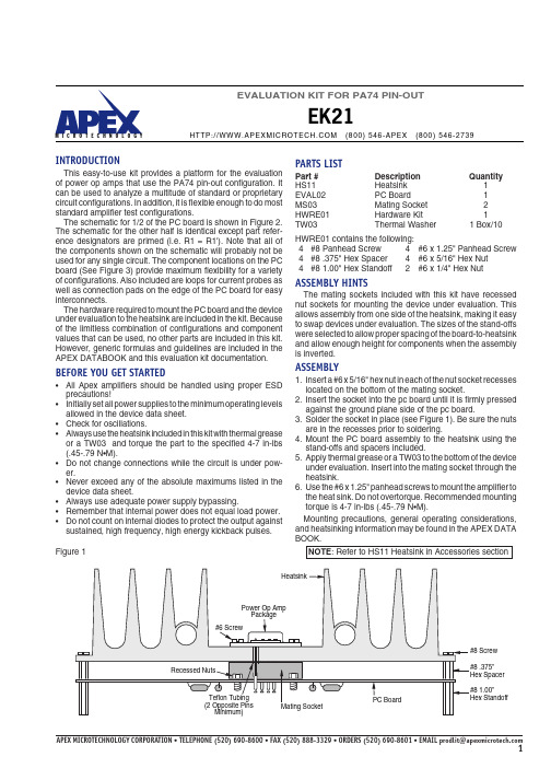
PARTS LIST
Part # HS11 EVAL02 MS03 HWRE01 TW03 Description Heatsink PC Board Mating Socket Hardware Kit Thermal Washer Quantity 1 1 2 1 1 Box/10
HWRE01 contains the following: 4 #8 Panhead Screw 4 #6 x 1.25" Panhead Screw 4 #8 .375" Hex Spacer 4 #6 x 5/16" Hex Nut 4 #8 1.00" Hex Standoff 2 #6 x 1/4" Hex Nut
BEFORE YOU GET STARTED
• All Apex amplifiers should be handled using proper ESD precautions! • Initially set all power supplies to the minimum operating levels allowed in the device data sheet. • Check for oscillations. • Always use the heatsink included in this kit with thermal grease or a TW03 and torque the part to the specified 4-7 in-lbs (.45-.79 N•M). • Do not change connections while the circuit is under power. • Never exceed any of the absolute maximums listed in the device data sheet. • Always use adequate power supply bypassing. • Remember that internal power does not equal load power. • Do not count on internal diodes to protect the output against sustained, high frequency, high energy kickback pulses. Figure 1
QC活动过程记录

项目
请购检漏用传感器
时间
7月20日-24日
地点
采供部
责任人
杨杰
7月20日填写请购单,告之采供部检漏用传感器厂家联系方式,按加急件程序办理,联系后确认到货时间为7月24日。
QC活动过程记录
项目
判断和解决炉体污染问题
时间
7月20日-24日
地点
热处理车间
责任人
全组
7月20日8:30抽真空至-0.083Mp。7月21日早上8:30,真空度为-0.083Mp,无漏气反馈,认真检查炉膛,炉砖干净,金属炉壁有少许材料挥发附着,用汽油清洗干净后。下午拆检机械泵与真空系统连接管道,管道内有灰份无油污,无真空返油现象,清洗管道,更换机械泵油。7月23日至7月24日用铜片试机4次,抽真空度至-0.083Mp,退火工艺为500℃/1h两次,600℃/1h一次和700℃/1h一次,全程按规程操作,7月23日(早上王静操作、下午朱峻昆操作)500℃/1h两次都抽真空至-0.083Mp,第二天均无漏气反馈,但铜片均呈退火异常色。每次试机后我们都清理了炉膛、料框。7月24日早上刘云600℃/1h退火前杨杰更换真空压力表后,材料退火出炉前表头有漏气反馈。700℃/1h(朱峻昆操作)一次退火,表头也有漏气反馈。结论是真空压力表损坏,真空系统漏气,排除炉体污染因素。
启动热检程序,升温至500℃全线检漏三次无漏点,升温至600℃全线检漏三次无漏点,升温至700℃全线检漏三次无漏点。降温过程穿插检漏三次无漏点。
QC活动过程记录
项目
分段排除
时间
8月10日-11日
地点
热处理车间
责任人
朱峻昆、杨杰
8月10日下午拆除增压泵连接,发现增压泵机械封闭装置锁闭不严,有微漏迹象,增压泵封闭阀门密封胶板也有裂纹,原因是增压泵封闭阀门密封胶板对裂纹在拆检其它部位时产生了位移,形成了漏点。真空检漏无法寻获漏点原因是抽真空管道连接密封好,漏气沿入了机械泵泵体,由于是沙眼缓漏,所以真空返油沉积在连接处,未进入真空炉体。联系上海电炉厂后,他们告之无增压泵机械封闭装置备件。我们就车制了两块定型钢板堵头,找了一块方型钢板打眼做增压泵阀门接口堵头,8月11日下午上机后,检漏无漏点,抽真空至-0.083Mp观察漏气反馈。
SR21-IR SR21-RG 手册说明书

SR21-IR / SR21-RGMANUALE ISTRUZIONICONTROLLILED DI USCITA (GIALLO)Il LED giallo acceso indica l’attivazione dell’uscita.DIMENSIONI D’INGOMBRO 1612POWER SUPPLYOUTPUTPer installare il sensore con il connettore a 90°, svitare la vite di bloccaggio e ruotare il blocchetto di fissaggio in senso antiorario; ad operazione conclusa riavvitare a fondo la vite di bloccaggio.CONNESSIONIConnettore M8DATI TECNICIPeso: 115 g. contrasto fra l’etichetta e il supporto. Il sensore può operare con la nuova impostazione. Una diversaindicazione segnala lo stato di errore a causa di un insufficiente contrasto rilevato. Impostazione statica del solo supporto (MANUALE)Adatta in condizioni meno critiche in cui l’etichetta risulta totalmente opaca e si desidera che l’uscita si attivi in corrispondenza dell’etichetta. Richiede l’acquisizione del solo supporto con posizionamento manuale.Passi di impostazione:1) Con led verde acceso in modo continuo, posizionare il supporto nella bocca del sensore, utilizzando per la centratura gli appositi riferimenti.2) Premere il tasto AUTO SET in modo breve. Il led verde e il led giallo si spengono. Inizia così la fase di acquisizione del supporto che non deve essere mosso finché il led verde non lampeggia in modo veloce. 3) Quando il led verde lampeggia, premere a lungo il tasto AUTO-SET fino a quando il led verde non lampeggia con tre lampi veloci intercalati da un pausa. A questo punto si può rilasciare il tasto.4) L'accensione continua del led verde READY indica che il sensore ha rilevato un grado sufficiente di trasparenza del supporto. Il sensore può operare con la nuova impostazione, attivando l’uscita in corrispondenza dell’etichetta (uscita NORMALE). Una diversa indicazione segnala lo stato di errore, a causa di una insufficiente trasparenza del supporto.Impostazione dinamica con uscita NORMALE o INVERTITALa programmazione deve avvenire durante il normale scorrimento del nastro delle etichette nella bocca del sensore. E’ adatta per etichette e supporti che hanno un grado di trasparenza abbastanza uniforme.Passi di impostazione: 1) Con led verde acceso in modo continuo, avviare lo scorrimento del nastro delle etichette nella boccadel sensore.2) Premere a lungo il tasto AUTO-SET fino a quando il led verde non comincia a lampeggiare in modolento.3) Rilasciato il pulsante, il sensore inizia ad acquisire il grado di trasparenza sia delle etichette che delsupporto in movimento, in cicli di circa 2 sec. Lasciare il sensore in questa fase di acquisizione per untempo abbastanza lungo da garantire il rilevamento del maggior numero di punti possibili. La durata di questa fase dipende dalla velocità del nastro e dalle dimensioni dell’etichette e del supporto. 4) Impostazione con uscita NORMALE: premere il tasto AUTO SET in modo breve. L'accensione continua del led verde READY indica che il sensore ha rilevato un grado sufficiente di contrasto fral’etichetta e il supporto. Il sensore inizia a operare con la nuova impostazione e l’uscita si attiva incorrispondenza dell’etichetta. Una diversa indicazione segnala lo stato di errore a causa di un insufficiente contrasto rilevato. 5) Impostazione con uscita INVERTITA: premere a lungo il tasto AUTO-SET fino a quando il led verdenon lampeggia con tre lampi veloci intercalati da un pausa. Rilasciato il pulsante, l'accensione continua del led verde READY indica che il sensore ha rilevato un grado sufficiente di contrasto fra l’etichetta e il supporto. Il sensore inizia a operare con la nuova impostazione e l’uscita si attiva in corrispondenza del supporto. Una diversa indicazione segnala lo stato di errore a causa di un insufficiente contrasto rilevato.INDICAZIONI DI ERRORE LED READY-ERROR lampeggiante alternativamente rosso e verde in modo lento: indica chel’impostazione (statica o dinamica) non ha avuto esito positivo per insufficiente trasparenza o contrastotra etichetta e supporto. In questo caso il sensore mantiene le impostazioni precedenti e può riprendere il normale funzionamento premendo e rilasciando il tasto AUTO-SET. LED READY-ERROR rosso lampeggiante a velocità media: durante il normale funzionamento e solocon uscita attiva, indica un cortocircuito o un sovraccarico delle uscite o una tensione di alimentazione insufficiente. L’indicazione scompare non appena viene rimossa la causa.BLOCCO E SBLOCCO DEL TASTOIl tasto può essere bloccato per evitare manovre accidentali durante il funzionamento normale del sensore. Il blocco è mantenuto anche dopo uno spegnimento e la successiva riaccensione del sensore. Le operazioni di blocco o di sblocco sono le seguenti: 1) A sensore spento premere e mantenere premuto il tasto AUTO-SET 2) Accendere il sensore tenendo sempre premuto il tasto. Il sensore inverte lo stato di blocco: se il tasto non era bloccato viene attivato il blocco e il led rosso si accende in modo continuo, se invece il tasto era già bloccato il sensore lo sblocca accendendo il led verde in modo continuo. 3) Il sensore comincia ad operare nel normale funzionamento impostato. Se il tasto è bloccato però non sarà possibile modificare l’impostazione fino al suo sblocco.Datalogic S.r.l.Via S. Vitalino 13 - 40012 Calderara di Reno - Italy Tel: +39 051 3147011 - Fax: +39 051 3147205 - Link utili disponibili su : Contatti, Termini e Condizioni, Supporto.Il periodo di garanzia per questo prodotto è di 36 mesi. Per maggiori dettagli vedere Condizioni Generali di Vendita su .In base alle vigenti normative nazionali ed europee, Datalogic non è tenuta allo smaltimento del prodotto alla fine del ciclo di vita. Datalogic consiglia di smaltire gli apparecchi attenendosi alle normative nazionali vigenti in materia di smaltimento dei rifiutio rivolgendosi agli appositi centri di conferimento.© 2007 - 2017 Datalogic S.p.A. e/o le sue consociate ♦ TUTTI I DIRITTI RISERVATI. ♦ Senza con ciò limitare i diritti coperti dal copyright,nessuna parte della presente documentazione può essere riprodotta, memorizzata o introdotta in un sistema di recupero o trasmessa in qualsiasi forma o con qualsiasi mezzo, o per qualsiasi scopo, senza l’espresso consenso scritto di Datalogic S.p.A. e/o delle sueconsociate. Datalogic e il logo Datalogic sono marchi registrati di Datalogic S.p.A. depositati in diversi paesi, tra cui U.S.A. e UE. Tutti glialtri marchi registrati e brand sono di proprietà dei rispettivi proprietari. Datalogic si riserva il diritto di apportare modifiche e/o miglioramentisenza preavviso.826003052 Rev.D。
fx21变频器说明书

fx21变频器说明书第一章:产品概述FX21变频器是一款先进的电力调节设备,应用于各种电动机的控制和调速,具有高效、稳定的特点。
本说明书将为用户详细介绍FX21变频器的特性、技术参数以及使用方法。
第二章:产品特性2.1 高效能:FX21变频器采用先进的PWM技术,将电能转换为电机所需的最佳功率,提高能源利用效率。
2.2 稳定性:内部采用高性能处理器和先进的控制算法,保证系统的稳定性和运行可靠性。
2.3 多功能性:FX21变频器具备多种控制模式和运行模式,可满足不同工况下的需求。
2.4 超载能力:具备良好的过载能力,适用于启动大型负载和瞬态过载的场景。
2.5 软启动:采用软启动技术,减少因突然启动对电网和电机的冲击。
2.6 超短路保护:具备内置短路保护功能,保护电机和设备的安全运行。
第三章:技术参数3.1 输入电压:220V/380V3.2 输出功率范围:0.75kW-315kW3.3 输出频率范围:0Hz-400Hz3.4 控制方式:V/F控制、矢量控制3.5 外观尺寸(宽*高*深):根据功率大小而定第四章:安装与接线4.1 安装环境要求:FX21变频器应安装在通风良好、温度适宜的环境中,避免阳光直射和湿度过高的地方。
4.2 接线方法:根据电气图进行正确接线,确保安全可靠。
第五章:操作说明5.1 开机操作:按下启动按钮,等待系统启动并进入待机状态。
5.2 运行参数调整:根据需要调整频率、转速等参数,通过界面操作和按键实现设置。
5.3 故障诊断:系统自带故障诊断功能,根据故障代码和报警信息进行排查和维修。
第六章:注意事项6.1 安全使用:在操作和维护过程中,要注意电器安全,避免触电和短路等危险。
6.2 维护保养:定期检查变频器的运行状态,及时清洁和维护,确保设备的正常运行。
附录:A. 故障代码对照表B. 电气图以上是FX21变频器的说明书内容,希望能够帮助用户了解和正确使用本产品。
如有更多问题,请参考附录中的故障代码对照表或联系我们的售后服务部门。
NEC SX-Aurora TSUBASA 系列超级计算机规格说明书
NEC Corporation(Headquarters) NEC Deutschland GmbH (HPC Europe)Vector Engine(VE) SpecificationsVector Supercomputer SX SeriesMail:***********Mail:***********•Speci cations and designs in this catalog are subject to change for improvement without notice.•All other products, brands, and trade names used in this document are trademarks or registered trademarks of their respective holders.Before using this product, please read carefully and comply with the cautions and warnings in manuals such as the Installation Guide and Safety Precautions. Incorrect use may cause a re, electrical shock, or injury.Please visit SX-Aurora TSUBASA website for all the lastest updates:For further information, please contact:SX-Aurora TSUBASA website/en/global/solutions/hpcSafety NoticeCat.No. E11-17100001EAs of October 2017.The new SX architecture contains the Vector Engine (VE) and Vector Host(VH). The VE executes complete applications while the VH mainlyprovides OS functions for connected VEs. The VE consists of one vectorprocessor with eight vector cores, using “high bandwidth memory”modules (HBM2) for utmost memory bandwidth. The world’s rstimplementation of one CPU LSI with six HBM2 memory modules using a“chip-on-wafer-on-substrate” technology (CoWoS) leads to theworld-record memory bandwidth of 1.2 TB/s.It is connected to the VH, a standard x86/Linux node, through PCIe. This newS X a r c h i t e c t u r e,w h i c hexecutes an entire applicationon the VE and the OS on theV H,c o m b i n e s h i g h e s tsustained performance, forwhich vector processors arefamous, in a well-knownx86/Linux environment.•Vector processor + x86/Linux architectureSupporting a GNU environment, the SX-Aurora TSUBASA offersFortran/C/C++ compilers with advanced automatic vectorization andparallelization for industry leading sustained performance and MPI librariesoptimized for system con gurations of the SX-Aurora TSUBASA.A supercomputer is a tool to increase the productivity of researchers anddevelopers. For users to achieve the optimal vector-processor performance,the SX-Aurora TSUBASA offers the following major software features:Inherited ease of use as a research and development tool•Compiler with automatic vectorization and parallelizationScienti c computing libraries optimized for SX-Aurora TSUBASA areavailable. These libraries include the industry standard BLAS, FFT, LAPACK,and ScaLAPACK.•Rich scientific computing libraryThe vector core on the VE processor is the most powerful single core in HPCas of today, thus keeping the design philosophy from the previous SX series.It will achieve industry leading calculation performance per core (307GFLOPS)*1 and memory bandwidth per core (150 GB/s)*1.With eight cores the vector processor will execute applications withextremely high sustained performance. It features 2.45 TF peak performanceand the world’s highest memory bandwidth per processor, 1.2 TB/s. Differentfrom standard processors a vector architecture is known to achieve asigni cant fraction of the peak performance on real applications.The vector processor employs 16nmF i n F E T p r o c e s s t e c h n o l o g y f o rextremely high performance and lowpower consumption.•Extremely high capability core and processor with extremely high memory bandwidth•State of the art technology forhigh sustained performanceVE cards with one vector-processor and high memory bandwidth HBM areused in a wide range of models. The product portfolio features a tower modelthat can be used on a user’s desk to a supercomputer model for alarge-scale supercomputer center. The product can be exibly con gured tomeet the most demanding computational needs.From entry model to supercomputer modelBroad supercomputer-applicable targetsBio, Healthcare, Drug discovery,Gene analysisAI, IoT, Image analysis, New energy Big data analytics, Finance,Next-generation distributionStructural analysis, Fluid analysis,New material developmentResearch and development,Large scale supercomputer centerClimate change, Weather forecast, Disaster preventionand mitigation, Resource explorationThe SX-Aurora TSUBASA offers up to 157 TF performance per rack and amemory bandwidth of up to 76 TB/s with 30 kW of power consumption,realizing 1/10 of the oor space and 1/5 of the power consumptioncompared to the predecessor SX-ACE.*2 This is a result of our innovationusing cutting edge LSI and packaging technologies such as the CoWoSimplementation, allowing for a thin wafer integration.10x space e ciency and 5x power e ciencySX-AuroraTSUBASA A500-64160TFLOPS10 racks•170KW157TFLOPS1 rack•30KW1/10 footprint1/5 PowerconsumptionNew SX architectureVHVector HostVEVector Engine*1: as of October, 2017 (according to NEC’s research), *2: Comparison in theoretical peak performanceVector EngineSX-Aurora TSUBASA series。
xb2bd21c技术参数
xb2bd21c技术参数全文共四篇示例,供读者参考第一篇示例:XB2BD21C技术参数XB2BD21C是一款高性能的操作按钮,广泛应用于各种电气控制系统中。
它具有高可靠性、灵活性和耐用性的特点,是电气控制系统中不可或缺的部件之一。
下面将详细介绍XB2BD21C的技术参数,以便更好地了解并使用这款操作按钮。
1. 电气参数XB2BD21C的额定电压为220VAC,并具有额定电流为10A的额定参数。
在使用过程中,需要确保电气参数符合要求,以保证设备的正常运行和安全使用。
2. 耐压能力XB2BD21C的绝缘耐压能力为2000VAC,这意味着操作按钮在设计范围内具有良好的绝缘性能,可以有效地避免电气短路等安全问题,保障设备和人员的安全。
3. 机械参数XB2BD21C的额定操作力为不超过50N,具有较小的操作力,操作按钮手感舒适。
其操作寿命达到了100万次以上,具有较长的使用寿命,可靠性高。
4. 环境参数XB2BD21C适用的环境温度范围为-25℃~+70℃,具有较广泛的工作温度范围,适用于各种恶劣的环境条件下工作。
操作按钮具有防尘、防水等功能,能够在恶劣的环境下正常工作。
5. 安装参数XB2BD21C的安装孔径为22mm,适用于标准的操作按钮安装孔尺寸。
其安装方式为拧紧方式,安装方便快捷,适用于各种设备。
第二篇示例:我们先从XB2BD21C的外观和尺寸参数开始介绍。
XB2BD21C采用标准的方形外壳设计,外观简洁美观,不占用过多空间。
其尺寸为22mm*22mm*17.5mm,适合安装在各种电气设备上,方便接线和操作。
接下来是XB2BD21C的电气参数。
该产品的额定电压为AC220V,额定电流为5A,具有较高的耐压和耐电流能力,适用于多种工业场合。
XB2BD21C还具有较低的触点电阻和较高的绝缘强度,能够确保稳定可靠的工作。
XB2BD21C还具有良好的机械参数。
其操作力为≤2.5N,释放力为≤0.3N,操作手感轻巧、灵敏。
FUJI xerox DocuWorks7文档处理软件 产品手册
DocuWorks 7文档处理解决方案本小册子中提及的其他名称都是相应公司的商标。
尽管所载信息在打印时正确无误,富士施乐亚太区保留随时更改所述机器规格参数而不另外通知的权利。
视产品购买所在国家或地区,规格参数、选件名称和供货情况可能会不尽相同。
“xerox”及连接的球体图形是施乐公司在美国和/或其它国家的标识或注册商标。
FXCL 1108富士施乐全国服务热线:800-820-5146 400-820-5146/富士施乐在华分支机构北京 北京市朝阳区建国路甲92号世茂大厦904室上海 上海市卢湾区淮海中路300号香港新世界大厦29F/30F/32F 广州 广州市东风中路410-412号时代地产中心15楼深圳 深圳市福田区益田路4068号卓越时代广场32楼01~08、10室成都 成都市锦江区滨江东路9号B 座香格里拉中心写字楼6层沈阳 沈阳市和平区南京北街206号城市广场第一座2-906天津 天津市南京路75号天津国际大厦502室长春 长春市南关区亚泰大街3218号通钢国际大厦A 座21层01室青岛 青岛市香港中路61号阳光大厦A 座30层E 、H 大连 大连市西岗区中山路147号森茂大厦1202E 哈尔滨 哈尔滨市南岗区民益街76号网通广场20楼杭州 杭州市江干区杭海路238号森禾商务广场A 座1903室、1904室武汉 武汉市建设大道568号新世界国贸大厦I 座21层2105-2107室长沙 长沙市雨花区韶山北路298号汇富中心A 栋1721室电话:010-********电话:021-********电话:020-********电话:0755-********电话:028-********电话:024-********电话:022-********电话:0431-********电话:0532-********/69电话:0411-********/61/80电话:0451-********电话:0571-********电话:027-********电话:0731-********郑州 郑州市中原中路220号裕达国际贸易中心A 座22层2212温州 温州市车站大道高联大厦11楼C6座合肥 合肥市濉溪路287号金鼎国际广场B 座2208室南京 南京市汉中路89号金鹰国际商城21层B2-C1座常州 常州市延陵西路23、25、27、29号投资广场17层1706单元无锡 无锡市中山路343号东方广场商务楼11层G 、H 座苏州 苏州市苏州工业园区苏华路2号国际大厦1610单元东莞 东莞市南城区元美路8号华凯广场A1113、A1115、A1116厦门 厦门市思明区湖滨东路6号华龙大厦805单元福州 福州市五四路国贸广场29层C2单元西安 西安市南关正街88号长安国际广场B 座1006室重庆 重庆市渝中区邹容路68号大都会商厦2301室昆明 昆明市北京路155号附1号红塔大厦1201室乌鲁木齐 乌鲁木齐市中山路86号中泉广场15楼G 座电话:0371-********电话:0577-********电话:0551-*******电话:025-********电话:0519-********电话:0510-********电话:0512-********电话:0769-********电话:0592-*******电话:0591-********电话:029-********电话:023-********电话:0871-*******电话:0991-*******DocuWorks 7文档处理解决方案一个能满足各种文档管理需求的解决方案DocuWorks 7 文档处理解决方案规格通过DocuWorks 的打印驱动程序导入支持的字符编码:Shift JIS(日文),KS C5601(韩文),GB2312(中文简体),Big 5(中文繁体),Windows-1252(西欧),TIS-620(泰文),Unicode在Microsoft Office XP/2003/2007(Word, Excel, PowerPoint) 中,可直接用插件按钮来转换为DocuWorks 文档。
ATA系列自动电源转换装置产品介绍说明书
ATA系列自动电源转换装置出众的整体解决方案 ATA—执行机构IZM9系列ATA 系列自动电源转换装置ATA 系列自动电源转换装置ATA 系列概述 ...................................................................................4型号说明 ...............................................................................5主要技术数据及性能指标 .................................................................6控制器 .................................................................................7电气线缆 ..............................................................................16执行断路器IZM9系列型号说明 ..............................................................................17脱扣器技术参数 ........................................................................18系统概览 ..............................................................................19可选附件 ..............................................................................23外形及安装尺寸 ........................................................................24系统电气图 ............................................................................48选型与订货 ............................................................................69订购指南 (73)ATA 系列执行断路器IZM9系列目录3ATA系列自动电源转换装置概述ATA系列产品描述伊顿的ATA系列自动转换开关装置,满足额定电压AC400V以下电源的自动转换。
- 1、下载文档前请自行甄别文档内容的完整性,平台不提供额外的编辑、内容补充、找答案等附加服务。
- 2、"仅部分预览"的文档,不可在线预览部分如存在完整性等问题,可反馈申请退款(可完整预览的文档不适用该条件!)。
- 3、如文档侵犯您的权益,请联系客服反馈,我们会尽快为您处理(人工客服工作时间:9:00-18:30)。
日本岛电FP21高性能-高精度0.1级PID调节器
█FP21调节器是日本岛电公司经典设计产品,投放中国市场已有超过15年的成功应用经历,经久不衰。
█双排大LED显示。
超大LCD显示屏,工作参数一目了然。
█9组曲线每组9段可编程,也可一组曲线81段可编程,可设定曲线连接次序、循环次数、运行时间。
█采用岛电专利的PID算法,9组PID参数,对应9组调节输出的上下限限幅,9组独立的报警组,以
对号入座的方式设到每段曲线上。
█伺服起动,曲线运行中的确保平台,断电保护,强制运行下一步曲线,数字滤波等功能。
█两组独立的报警继电器可设三种类型十种报警方式,并能进一步设定报警回差,可设定继电器动作灵敏度参数防止继电器误动作。
█8组外部DI输入,程序的运行、跳步、保持等复杂的键操作通过外部DI被简化。
10组DO输出,4组时标输出,可对应运行状态输出,完成诸如开关炉门等的辅助控制。
█数字通讯接口(选件),RS232C或RS422,配合XIMADEN2008中文组态软件与上位机组成小型DCS控制系统。
█模拟变送输出(选件):用于现场记录数据。
还可与SR25、SR253组成经典的三温区可编程精确控温。