MDVP definition
mdp文件详解
mdp文件详解title = BPTI in water, 300K ;名字cpp = /lib/cpp ;预处理程序,gcc的路径define = -DPOSRES_LIPID ;对top文件的控制选项-DFLEXBLE:这个选项告诉grompp水分子是柔性的,非刚体-DPOSRES:限制自由度;constraints = all-bondsintegrator = md ;算法,md这里表示蛙跳算法dt = 0.001 ; ps ! ;时间步长nsteps = 1000 ; total 10 ps. ;步数comm_mode = None ;linear对质心平动,anglar 平动+转动,none对质心无限制nstxout = 0 ;将坐标写入输出轨迹文件的频率nstvout = 0 ;将速度写入输出轨迹文件的频率nstfout = 0 ;将力写入输出轨迹文件的频率nstxtcout = 500 ;将坐标写日xtc坐标文件的频率nstlog = 1000 ;将能量写入log文件的频率nstenergy = 1000 ;将能量写入energy文件的频率nstlist = 10 ;neighbor list 的更新频率ns_type = grid ;neighbor search 的种类,分两种grid:格子和simple coulombtype = PME ;库伦作用种类,cut-off,ewald,PME,PPPM.... rlist = 1.0 ;短程neighbor-list截断半径rcoulomb = 1.0 ;库伦截断半径rvdw = 1.0 ;范德华力截断半径; Berendsen temperature coupling is on in two groupsTcoupl = berendsen ;热浴?berendsen和nose-hoovertc-grps = CNT SOL ;分别进行热浴的类tau_t = 0.1 0.1 ;热浴时间常数(ps)ref_t = 300 300 ;热浴的参考温度(对不同的类分别指定); Energy monitoringenergygrps = CNT SOL; non-equilibrium MDfreezegrps = CNT ;指出受约束的系统freezedim = Y Y Y ;Y=yes,N=no,三个字母分别代表xyz轴; Isotropic pressure coupling is now on;Pcoupl = berendsen ;NO:无压力耦合,盒子尺寸大小固定,berendsen:每个时间步长都会重新度量盒子大小,Parrinello-Rahman;Pcoupltype = semiisotropic;tau_p = 1.0 1.0 ;耦合时间常数;compressibility = 0 4.5e-5 ;压缩系数;ref_p = 1.0 1.0 ;参考压强; Generate velocites is off at 300 K.gen_vel = no ;no:初始速度为零yes:按照麦克斯韦分布设定初始速度gen_temp = 300.0 ;麦克斯韦分布的温度gen_seed = 173529 ;使用随机发生器来产生随机速度(time() + getpid()) % 1000000。
DMVPN技术详解
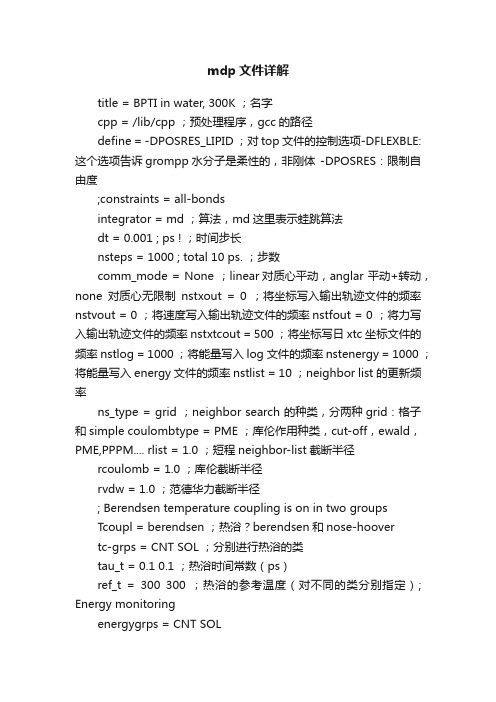
一方面会向hub获取其他站点的地址,从而建立终端间的隧道。 • spoke注册后,hub和多个spoke已建立永久隧道,此时spoke之间想要直接通信,会像hub解析其他的spoke的地址,直接建立
隧道(有流量则建立,无流量则拆除)。 • spoke和hub间可以传输单播和组播报文,spoke和spoke间只能传输单播(无法运行路由协议)。 DM-VPN(动态多点VPN):
hub点发出的路由不会将下一跳置为自己而会带真实下一跳从而使多个分支直接通信路由直通不必在hub中转r2configifnoipnexthopselfeigrp1?层次化网络设计12开启nhrp重定向分支内网设备向分支内网设备发送数据第一次像hub做请求hub会发送重定向信息给分支1和分支2两个分支内网设备会互相请求对方的nhrp信息动态建立隧道
分区 文档备份 的第 1 页
4. ipsec
R1无需做配置,直连可保证tunnel通。 • mGRE:
○ R2(HUB): R2(config)#int tunnel 1 R2(config-if)#tunnel mode gre multipoint R2(config-if)#tunnel source e1/0 R2(config-if)#ip address 100.1.1.2 255.255.255.0
mGRE NHRP DMVPN
2015年6月17日 19:31
GRE: • GRE依赖目的地址,所以只能支持点到点隧道,MGRE的可以实现点到多点。 • MGRE封装和GRE相同。 • spoke路由器只需知道hub路由器的地址,即可建立MGRE。 • MGRE依赖NHRP工作。
NHRP:
• NHRP能够动态学习其他站点的NBMA地址。 • hub路由器会维护一个NHRP数据库(tunnelபைடு நூலகம்NBMA地址的映射),spoke路由器启动后,一方面会注册自己的NBMA地址,
Loadline & transient definition.0327

edit by sue xu 07/03/27
Outline
• • • • What is VRM/VRD? What is FMB? The reason for doing Load line ? Relationship between transient & load line .
socket load line equation 1:VCCMAX socket load line equation 2:Vcctyp socket load line equation 3:Vccmin socket load line
equation Vcc=VID-(RLL*ICC) Vcc=VID-TOB-(RLL*ICC) Vcc=VID-2*TOB-(RLL*ICC)
• ESR is too big
• Capacitance is not enough
775_VR_CONFIG_06B Specification Input Parameters
The relationship between load line and transient
loadline&thermal
Transient waveform
Transient waveform judgement
Loadline:
Vo Vmax Vtyp Vmin TOB
Io
The upper and lower load lines represent the allowable range of voltages that must be presented to the processor.the voltage must always stay within these boundaries for proper operation of the processor.
MSDP(组播源发现协议)

MSDP(组播源发现协议)当网络跨越了公网,或者网络需要各自独立时,如果每个独立的网络,或者是每个AS之间都需要组播通信的情况下,我们需要在不影响网络独立的前提下连通网络间的组播。
不各个独立的网络中,又希望自己的组播路由器可以由自己完全控制,那么就需要将各个网络配置成独立的PIM-SM域。
要将不同的PIM-SM域之间连通组播,就必须先有正常的组播树,而PIM-SM组播树的建立,必须了解到网络中的RP 信息,以及组播源的位置。
要连通不同的PIM-SM域,就必须在域之间建立MSDP 连接,MSDP在PIM-SM域间传递组播源的信息,以及保持域间RP的信息。
在使用MSDP将多个PIM-SM域连接时,每一个PIM-SM都可以在域中配置各自的RP,以实现自治。
在不同的PIM-SM域之间建立MSDP连接时,是使用TCP 639,IP地址高的初始化TCP连接,60秒一次keepalive,75秒后没数据或keepalive则重建TCP。
建立连接的双方均是各自区域的RP,组播源向RP注册之后,那么RP将这些源信息通过在MSDP 连接上发送Source-Active (SA)到远程RP,以提供组播源的信息。
因为RP收到Source-Active (SA)后,也是要做RPF检测的,检测是根据BGP来做的,在这里,需要使用MP-BGP之组播MP-BGP,组成员的网络信息和建立MSDP连接的peer地址理论上都需要在MP-BGP中进行通告,一是防止RPF检测失败,二是由此来决定组播数据的传递,所以十分重要。
但是如果不需要在PIM-SM域之间开启MP-BGP,就会有RPF检测失败的危险,失败后,Source-Active (SA)将被丢弃,所以要想在不开启MP-BGP的情况下,又要接收所有的Source-Active (SA),则将接收端配置成default MSDP,那么该域将接收任何SA 信息。
在配置default MSDP时,需要指定从何处接收SA,就需要指定对端MSDP peer,使用ip msdp default-peer指定,之后从对端过来的SA将不做RPF检测而完全被接收。
TSL UMD Protocol

TSL UMD ProtocolIntroductionThe TSL protocols are widely implemented throughout the industry, especially for Multiviewer use.There is no charge for the use of these protocols.•UMD V3.1 is the TSL basic industry standard serial protocol.•UMD V4.0 extends the basic V3.1 protocol to add full control of text and tally lamp colours.These two protocols can also be implemented over UDP/IP where each UDP packet contains one serial data packet.•UMD V5.0 is a new protocol, specifically aimed at multiviewer display devices, over Ethernet.The following document describes these protocols.Note these protocols are published without technical support; however In case of difficulty please email tim.whittaker@.Protocol V3.11.0 ScopeThis protocol sets out to define the method of communication between a TSL controller and peripheral devices on a multi-drop device bus.The protocol described is for one way communication only. It details physical layer, link layer and message structure.2.0 ElectricalRS 422/ RS 4858 bit data1 stopeven parity38k4 baud3.0 Dynamic UMD Protocol----------------------------------------------------------------| HEADER | CONTROL BYTE | DISPLAY DATA |----------------------------------------------------------------Header = Display address (0-126) + 80 hex(1 byte) ( control byte and display datawill be sent )Control bit 0 = tally 1 ( 1=on, 0=off )(1 byte) bit 1 = tally 2 ( 1=on, 0=off )bit 2 = tally 3 ( 1=on, 0=off )bit 3 = tally 4 ( 1=on, 0=off )bits 4-5 = brightness databit 4 = 0, bit 5 = 0 (0 brightness)bit 4 = 0, bit 5 = 1 (1/7 brightness)bit 4 = 1, bit 5 = 0 (1/2 brightness)bit 4 = 1, bit 5 = 1 (full brightness)bit 6 = reserved (clear to 0)bit 7 = cleared to 0Display Data = 16 displayable ASCII characters(16 bytes) in the range 20 hex to 7E hex.All 16 characters must be sent.4.0 Single Dynamic DisplaysFor 8 character displays only the first 8 characters of thedisplay data are used, the remaining 8 are needed just forpadding.Only tallies 1&2 are use for single displays.5.0Dual Dynamic DisplaysDual 8 character displays are treated as a single display of16 characters, the first 8 characters for the left-hand sideand the second 8 characters for the right-hand side.Tallies 1&2 are for the left display and tallies 3&4 for theright display.6.0 Triple/Quad Dynamic DisplaysThese units take two addresses.Address 1, for display 1, tally 1 & 2Address 1 for display 2, tally 3 & 4Address 2 for display 3, tally 5 & 6Address 2 for display 4, tally 7 & 8Protocol V4.0Summary of EnhancementsTo support multiple tally channels, more tally control bits are added. Full compatibility withV3.1 (1994) is maintained. Future revisions provided for with version/byte count information. V3.1 HeaderThe current format is retained up to and including the final character of the data field;<0x80+addr><CTRL><DATA>where CTRL is :bit 7: 0bit 6: 0 for display data, 1 for command databit 5: brightness MSBbit 4: brightness LSBbit 3: tally 3bit 2: tally 2bit 1: tally 1bit 0: tally 0and DATA is:16 ASCI characters for messages with CTRL.6 = 0 (i.e. display data messages)For CTRL.6=1, DATA is defined by the control code formed by CTRL5:0.NB Version 4.0 enhancements only apply to display data messages; command messages are V4.0 EnhancementsV4.0 and above messages are recognised as having further data following the last byte of<DATA>, as follows:<0x80+addr><CTRL><DATA><CHKSUM><VBC><XDATA>CHKSUM = (2’s complement of (sum of all V3.1 bytes)) modulo 128(i.e. hdr+CTRL+DATA)VBC is:Bit 7: 0Bit 6-4: minor Version (V4.0 = 0)Bit 3-0 Byte count of XDATA<XDATA> is defined by minor Version number.Currently the following is defined:-Minor Version = 0 (i.e. V4.0)XDATA consists of 2 bytes:Xbyte 1 has 6 tally bits for Display L, Xbyte 2 has 6 tally bits for display R.The 6 bits consist of 2 bits each for the LH tally, text, and RH tally as follows:Bit 7 0Bit 6 Reserved (ignore (RX) or set to 0 (TX))Bit 5: LH MSBBit 4: LH LSBBit 3: Txt MSBBit 2: Txt LSBBit 1: RH MSBBit 0: RH LSB2 Bit values are:0 = OFF; 1 = RED, 2 = GREEN, 3 = AMBER.The four original V3.1 tally bits (in the CTRL packet) are now separately mapped to the four parallel tally outputs from the display.Protocol V5.0OverviewThis protocol is a new 16 bit UMD protocol, with no reverse compatibility to previous TSL UMD protocols.The primary points for this protocol to provide over previous versions are as follows:1. Display addressing up to 65,535 per screen2. ASCII or Unicode character sets3. Variable length mnemonics4. IP based packet communication, with optional wrapper for stream based comms5. Multiple display updates per packetPhysical LayerPackets are sent via UDP. Maximum packet length is 2048 bytes.Optionally, the protocol can operate over TCP/IP, or any other byte stream interface, with the following wrapper scheme:DLE is defined as 0xFESTX is defined as 0x02Packet start is delimited by the sequence DLE/STX.Any occurrence of the DLE character in the packet is byte stuffed to DLE/DLE.Any byte count fields in the packet are not affected by the byte stuffing.Message Format16 bit values are sent as little-endian, i.e. LSB/MSB.The packet is defined as follows:PBC / VER / FLAGS / SCREEN / (<DMSG> ( / <DMSG>)…) or (SCONTROL)PBC (16 bit):Total byte count of following packetVER (8 bit):Minor version number (e.g. V5.00, VER = 0). Note this byte can be used as versioning control for the following definitions. Whilst any future changes to this protocol will aim to be backward compatible, this is not guaranteed.FLAGS (8 bit):Defined as follows:Bit 0: Clear for ASCII based strings in packet, set for Unicode UTF-16LEBit 1: If set, data after SCREEN is screen control data (SCONTROL) – otherwise it’s display message data (DMSG)Bit 2-7: Reserved (clear to 0)SCREEN (16 bit):Primary index for use where each screen entity would have display indices (defined below) starting from 0.Index 0xFFFF is reserved as a “Broadcast” to all screens.If not used, set to 0.Display Message (<DMSG>) DefinitionThis message definition is sent per display, and there can be several in a packet (up to max packet length). Constructed as follows:INDEX / CONTROL / (LENGTH / TEXT) or (CONTROL DATA)INDEX (16 bit):The 0 based address of the display, up to 65534 (0xFFFE). Address 0xFFFF is reserved as a “Broadcast” address to all displays.CONTROL (16 bit):Display control and tally data as follows:Bit 0-1: RH Tally Lamp stateBit 2-3: Text Tally stateBit 4-5: LH Tally Lamp stateBit 6-7: Brightness value (range 0-3)Bit 8-14: Reserved (clear to 0)Bit 15: Control Data: following data to be interpreted as Control data ratherthan Display data when set to 1.2 Bit Tally values are:0 = OFF, 1 = RED, 2 = GREEN, 3 = AMBER.Display Data: (CONTROL bit 15 is cleared to 0)LENGTH (16 bit):Byte count of following text.TEXT:UMD text, format defined by FLAGS byte.Control Data: (CONTROL bit 15 is set to 1)Not defined in this version of protocol.Screen control (SCONTROL) Definition (FLAGS bit 1 is set to 1)Not defined in this version of protocol.。
ksz8851-16mll_ds芯片手册

KSZ8851-16MLL/MLLI/MLLUSingle-Port Ethernet MAC Controllerwith 8-Bit or 16-Bit Non-PCI InterfaceRevision 2.2General DescriptionThe KSZ8851M-series is a single-port controller chip witha non-PCI CPU interface and is available in 8-bit and 16-bit bus designs. This datasheet describes the 48-pin LQFPKSZ8851-16MLL for applications requiring high-performance from single-port Ethernet Controller with 8-bitor 16-bit generic processor interface. The KSZ8851-16MLL offers the most cost-effective solution for addinghigh-throughput Ethernet connectivity to traditionalembedded systems.The KSZ8851-16MLL is a single chip, mixed analog/digitaldevice offering Wake-on-LAN technology for effectivelyaddressing Fast Ethernet applications. It consists of a fastEthernet MAC controller, an 8-bit or 16-bit generic hostprocessor interface and incorporates a unique dynamicmemory pointer with 4-byte buffer boundary and a fullyutilizable 18KB for both TX (allocated 6KB) and RX(allocated 12KB) directions in host buffer interface.The KSZ8851-16MLL is designed to be fully compliant withthe appropriate IEEE 802.3 standards. An industrialtemperature-grade version of the KSZ8851-16MLLI and aqualified AEC-Q100 Automotive version of the KSZ8851-16MLLU are also available (see “Ordering Information”section).LinkMD®Physical signal transmission and reception are enhancedthrough the use of analog circuitry. This makes the designmore efficient and allows lower-power consumption. TheKSZ8851-16MLL is designed using a low-power CMOSprocess that features a single 3.3V power supply withoptions for 1.8V, 2.5V or 3.3V VDD I/O. The deviceincludes an extensive feature set that offers managementinformation base (MIB) counters and CPU control/datainterfaces with single shared data bus timing.The KSZ8851-16MLL includes a unique cable diagnosticsfeature called LinkMD®. This feature determines the lengthof the cabling plant and also ascertains if there is an openor short condition in the cable. Accompanying softwareenables the cable length and cable conditions to beconveniently displayed. In addition, the KSZ8851-16MLLsupports Hewlett Packard (HP) Auto-MDIX therebyeliminating the need to differentiate between straight orcrossover cables in applications.Functional DiagramFigure 1. KSZ8851-16MLL/MLLI Functional DiagramFeatures•Integrated MAC and PHY Ethernet Controller fully compliant with IEEE 802.3/802.3µ standards •Designed for high performance and high throughput applications•Supports 10BASE-T/100BASE-TX•Supports IEEE 802.3x full-duplex flow control and half-duplex backpressure collision flow control •Supports DMA-slave burst data read and write transfers•Supports IP Header (IPv4)/TCP/UDP/ICMP checksum generation and checking•Supports IPv6 TCP/UDP/ICMP checksum generation and checking•Automatic 32-bit CRC generation and checking •Simple SRAM-like host interface easily connects to most common embedded MCUs.•Supports multiple data frames for receive without address bus and byte-enable signals•Supports both Big- and Little-Endian processors •Larger internal memory with 12K Bytes for RX FIFO and 6K Bytes for TX FIFO. Programmable low, highand overrun watermark for flow control in RX FIFO •Shared data bus for Data, Address and Byte Enable •Efficient architecture design with configurable host interrupt schemes to minimize host CPU overhead and utilization•Powerful and flexible address filtering scheme •Optional to use external serial EEPROM configuration for MAC address•Single 25MHz reference clock for both PHY and MAC •HBM ESD Rating 6kVPower Modes, Power Supplies, and Packaging •Single 3.3V power supply with options for 1.8V, 2.5V and 3.3V VDD I/O•Built-in integrated 3.3V or 2.5V to 1.8V low noise regulator (LDO) for core and analog blocks •Enhanced power management feature with energy detect mode and soft power-down mode to ensurelow-power dissipation during device idle periodsComprehensive LED indicator support for link, activity and 10/100 speed (2 LEDs) - User programmable •Low-power CMOS design•Commercial Temperature Range: 0°C to +70°C •Industrial Temperature Range: –40°C to +85°C •Flexible package options available in 48-pin (7mm × 7mm) LQFP KSZ8851-16MLL or 128-pinPQFP KSZ8851-16/32MQLAdditional FeaturesIn addition to offering all of the features of a Layer 2 controller, the KSZ8851-16MLL offers:•Flexible 8-bit and 16-bit generic host processor interfaces with same access time and single bustiming to any I/O registers and RX/TX FIFO buffers •Supports to add two-byte before frame header in order for IP frame content with double word boundary •Micrel LinkMD® cable diagnostic capabilities to determine cable length, diagnose faulty cables, anddetermine distance to fault•Wake-on-LAN functionality– Incorporates Magic Packet™, wake-up frame, network link state, and detection of energy signaltechnology•HP Auto MDI-X™ crossover with disable/enable option •Ability to transmit and receive frames up to 2000 bytes Network Features•10BASE-T and 100BASE-TX physical layer support •Auto-negotiation: 10/100 Mbps full and half duplex •Adaptive equalizer•Baseline wander correctionApplications•Video/Audio Distribution Systems•High-end Cable, Satellite, and IP set-top boxes •Video over IP and IPTV•Voice over IP (VoIP) and Analog Telephone Adapters (ATA)•Industrial Control in Latency Critical Applications •Home Base Station with Ethernet Connection •Industrial Control Sensor Devices (Temperature, Pressure, Levels, and Valves)•Security, Motion Control and Surveillance Cameras •In-vehicle Diagnostics (OBD) & software download Markets•Fast Ethernet•Embedded Ethernet•Industrial Ethernet•Embedded Systems•Automotive EthernetOrdering InformationPart Number Temperature Range Package Lead Finish KSZ8851-16MLL 0°C to 70°C 48-Pin LQFP Pb-Free KSZ8851-16MLLI –40°C to +85°C 48-Pin LQFP Pb-Free KSZ8851-16MLLU(Automotive AEC-Q100 qualified)–40°C to +85°C 48-Pin LQFP Pb-Free KSZ8851-16MLL-Eval Evaluation Board for the KSZ8851-16MLLRevision HistoryRevision Date Summary of Changes1.0 06/30/2008 First released Information.1.1 2/13/2009 Improved EDS Rating up to 6KV, revised Ordering Information and Updated Table content and description.2.0 8/31/2009 Change revision ID from “0” to “1” in CIDER (0xc0) register. Update pins 8, 14 and 29 description for 1.8V VDD_IO supply. To add the command write (CMD=1) address index register in order for software to read back the CMD register value. To enable software read or write external EEPROM.2.104/30/2012 In 16-bit bus mode, the SD1 bit must set to “1” when CMD = 1 during DMA access. Remove auto-enqueue function, add the reset circuit. Update the description for the register PMECR Bits [1,0]. Add KSZ8851MLLU Automotive part. Add the description for the register TXCR bit 7. Update read/write timing diagram for Asynchronous Cycle. Add power sequence descriptions in the reset timing section.2.203/04/2014 Remove auto-enqueue function for transmit, Update the description for section of Asynchronous Interface. Update read/write timing diagram and table, add notes for timing table ,CIDER and RXFCTR registers. Update the defination for Register P1CR bit [9],P1MBCR bit [4] and RX/TX pair. Update the description in Half-Duplex Backpressure section. Change TTL to CMOS and updates min/max I/O voltage in different VDDIO.ContentsList of Figures (7)List of Tables (8)Pin Configuration (9)Pin Description (10)Pin for Strap-In Options (13)Functional Description (14)Functional Overview (14)Rx unused block disabled (14)Wake-up Packet (16)Physical Layer Transceiver (PHY) (17)Straight Cable (18)Crossover Cable (19)Access (21)Usage (21)Frame Queue (RXQ) Frame Format (29)EEPROM Interface (31)CPU Interface I/O Registers (33)I/O Registers (33)Internal I/O Registers Space Mapping (33)CIDER (37)0x887x (37)Reserved (38)Do Not Care (38)None (38)Register Map: MAC, PHY and QMU (39)Bit Type Definition (39)0x00 – 0x07: Reserved (39)Chip Configuration Register (0x08 – 0x09): CCR (39)0x0A – 0x0F: Reserved (39)Host MAC Address Registers: MARL, MARM and MARH (40)Host MAC Address Register Low (0x10 – 0x11): MARL (40)Host MAC Address Register Middle (0x12 – 0x13): MARM (40)Host MAC Address Register High (0x14 – 0x15): MARH (40)0x16 – 0x1F: Reserved (40)On-Chip Bus Control Register (0x20 – 0x21): OBCR (41)EEPROM Control Register (0x22 – 0x23): EEPCR (41)Memory BIST Info Register (0x24 – 0x25): MBIR (42)Global Reset Register (0x26 – 0x27): GRR (42)0x28 – 0x29: Reserved (42)Wakeup Frame Control Register (0x2A – 0x2B): WFCR (43)0x2C – 0x2F: Reserved (43)Wakeup Frame 0 CRC0 Register (0x30 – 0x31): WF0CRC0 (43)Wakeup Frame 0 CRC1 Register (0x32 – 0x33): WF0CRC1 (43)Wakeup Frame 0 Byte Mask 0 Register (0x34 – 0x35): WF0BM0 (44)Wakeup Frame 0 Byte Mask 1 Register (0x36 – 0x37): WF0BM1 (44)Wakeup Frame 0 Byte Mask 2 Register (0x38 – 0x39): WF0BM2 (44)Wakeup Frame 0 Byte Mask 3 Register (0x3A – 0x3B): WF0BM3 (44)0x3C – 0x3F: Reserved (44)Wakeup Frame 1 Byte Mask 0 Register (0x44 – 0x45): WF1BM0 (45)Wakeup Frame 1 Byte Mask 1 Register (0x46 – 0x47): WF1BM1 (45)Wakeup Frame 1 Byte Mask 2 Register (0x48 – 0x49): WF1BM2 (45)Wakeup Frame 1 Byte Mask 3 Register (0x4A – 0x4B): WF1BM3 (45)0x4C – 0x4F: Reserved (45)Wakeup Frame 2 CRC0 Register (0x50 – 0x51): WF2CRC0 (45)Wakeup Frame 2 CRC1 Register (0x52 – 0x53): WF2CRC1 (46)Wakeup Frame 2 Byte Mask 0 Register (0x54 – 0x55): WF2BM0 (46)Wakeup Frame 2 Byte Mask 1 Register (0x56 – 0x57): WF2BM1 (46)Wakeup Frame 2 Byte Mask 2 Register (0x58 – 0x59): WF2BM2 (46)Wakeup Frame 2 Byte Mask 3 Register (0x5A – 0x5B): WF2BM3 (46)0x5C – 0x5F: Reserved (46)Wakeup Frame 3 CRC0 Register (0x60 – 0x61): WF3CRC0 (46)Wakeup Frame 3 CRC1 Register (0x62 – 0x63): WF3CRC1 (47)Wakeup Frame 3 Byte Mask 0 Register (0x64 – 0x65): WF3BM0 (47)Wakeup Frame 3 Byte Mask 1 Register (0x66 – 0x67): WF3BM1 (47)Wakeup Frame 3 Byte Mask 2 Register (0x68 – 0x69): WF3BM2 (47)Wakeup Frame 3 Byte Mask 3 Register (0x6A – 0x6B): WF3BM3 (47)0x6C – 0x6F: Reserved (47)Transmit Control Register (0x70 – 0x71): TXCR (48)Transmit Status Register (0x72 – 0x73): TXSR (49)Receive Control Register 1 (0x74 – 0x75): RXCR1 (49)Receive Control Register 2 (0x76 – 0x77): RXCR2 (50)TXQ Memory Information Register (0x78 – 0x79): TXMIR (51)0x7A – 0x7B: Reserved (51)Receive Frame Header Status Register (0x7C – 0x7D): RXFHSR (51)Receive Frame Header Byte Count Register (0x7E – 0x7F): RXFHBCR (52)TXQ Command Register (0x80 – 0x81): TXQCR (52)RXQ Command Register (0x82 – 0x83): RXQCR (53)TX Frame Data Pointer Register (0x84 – 0x85): TXFDPR (54)RX Frame Data Pointer Register (0x86 – 0x87): RXFDPR (54)0x88 – 0x8B: Reserved (55)RX Duration Timer Threshold Register (0x8C – 0x8D): RXDTTR (55)RX Data Byte Count Threshold Register (0x8E – 0x8F): RXDBCTR (55)Interrupt Enable Register (0x90 – 0x91): IER (55)Interrupt Status Register (0x92 – 0x93): ISR (56)0x94 – 0x9B: Reserved (57)RX Frame Count & Threshold Register (0x9C – 0x9D): RXFCTR (57)TX Next Total Frames Size Register (0x9E – 0x9F): TXNTFSR (57)MAC Address Hash Table Register 0 (0xA0 – 0xA1): MAHTR0 (58)MAC Address Hash Table Register 1 (0xA2 – 0xA3): MAHTR1 (58)MAC Address Hash Table Register 2 (0xA4 – 0xA5): MAHTR2 (58)MAC Address Hash Table Register 3 (0xA6 – 0xA7): MAHTR3 (58)0xA8 – 0xAF: Reserved (58)Flow Control Low Watermark Register (0xB0 – 0xB1): FCLWR (58)Flow Control High Watermark Register (0xB2 – 0xB3): FCHWR (59)Flow Control Overrun Watermark Register (0xB4 – 0xB5): FCOWR (59)0xB6 – 0xBF: Reserved (59)Chip ID and Enable Register (0xC0 – 0xC1): CIDER (59)0xC2 – 0xC5: Reserved (59)0xCA – 0xCF: Reserved (60)Indirect Access Data Low Register (0xD0 – 0xD1): IADLR (60)Indirect Access Data High Register (0xD2 – 0xD3): IADHR (60)Power Management Event Control Register (0xD4 – 0xD5): PMECR (61)Go-Sleep and Wake-Up Time Register (0xD6 – 0xD7): GSWUTR (62)PHY Reset Register (0xD8 – 0xD9): PHYRR (62)0xDA – 0xDF: Reserved (62)0xE0 – 0xE3: Reserved (62)PHY 1 MII-Register Basic Control Register (0xE4 – 0xE5): P1MBCR (63)PHY 1 MII-Register Basic Status Register (0xE6 – 0xE7): P1MBSR (64)PHY 1 PHY ID Low Register (0xE8 – 0xE9): PHY1ILR (64)PHY 1 PHY ID High Register (0xEA – 0xEB): PHY1IHR (64)PHY 1 Auto-Negotiation Advertisement Register (0xEC – 0xED): P1ANAR (65)PHY 1 Auto-Negotiation Link Partner Ability Register (0xEE – 0xEF): P1ANLPR (66)0xF0 – 0xF3: Reserved (66)Port 1 PHY Special Control/Status, LinkMD (0xF4 – 0xF5): P1SCLMD (66)Port 1 Control Register (0xF6 – 0xF7): P1CR (67)Port 1 Status Register (0xF8 – 0xF9): P1SR (68)0xFA – 0xFF: Reserved (69)MIB (Management Information Base) Counters (70)Absolute Maximum Ratings (73)Operating Ratings (73)Electrical Characteristics (73)Timing Specifications (75)Asynchronous Read and Write Timing (Processor read and write) (75)Selection of Isolation Transformers (80)Selection of Reference Crystal (80)Package Information (81)Acronyms and Glossary (82)Figure 2. 48-Pin LQFP (9)Figure 3. Typical Straight Cable Connection (18)Figure 4. Typical Crossover Cable Connection (19)Figure 5. Auto Negotiation And Parallel Operation (20)Figure 6. Ksz8851-16mll 8-Bit And 16-Bit Data Bus Connections (25)Figure 8. Host Rx Single Or Multiple Frames In Auto-Dequeue Flow Diagram (30)Figure 9. Phy Port 1 Near-End (Remote) And Host Far-End (Local) Loopback Paths (32)Figure 10. Asynchronous Cycle (75)Figure 11. Auto Negotiation Timing (76)Figure 12. Reset Timing (77)Figure 13. Eeprom Read Cycle Timing Diagram (78)Figure 14. Recommended Reset Circuit (79)Figure 15. Recommended Circuit For Interfacing with Cpu/Fpga Reset (79)Table 1. Internal Function Blocks Status (14)Table 2. Mdi/Mdi-X Pin Definitions (18)Table 3. Address Filtering Scheme (23)Table 4. Bus Interface Unit Signal Grouping (24)Table 5. Frame Format For Transmit Queue (26)Table 6. Transmit Control Word Bit Fields (26)Table 7. Transmit Byte Count Format (27)Table 8. Registers Setting For Transmit Function Block (27)Table 9. Frame Format For Receive Queue (29)Table 10. Registers Setting For Receive Function Block (29)Table 11. Ksz8851-16mll Eeprom Format (31)Table 12. Format Of Mib Counters (70)Table 13. Port 1 Mib Counters Indirect Memory Offsets (71)Table 14. Asynchronous Cycle Timing Parameters (75)Table 15. Auto Negotiation Timing Parameters (76)Table 16. Reset Timing Parameters (77)Table 17. Eeprom Timing Parameters (78)Table 18. Transformer Selection Criteria (80)Table 19. Qualified Single Port Magnetics (80)Table 20. Typical Reference Crystal Characteristics (80)Figure 2. 48-Pin LQFPPin Number Pin Name Type Pin Function1 P1LED1 IPU/O Programmable LED output to indicate port activity/status.LED is ON when output is LOW; LED is OFF when output is HIGH.Port 1 LED indicators1 defined as follows:Chip Global Control Register: CGCR bit [9]0 (Default) 1P1LED1 100BT ACTP1LED0 LINK/ACT LINK1. Link = LED On; Activity = LED Blink; Link/Act = LED On/Blink;Speed = LED On (100BASE-T); LED Off (10BASE-T)Config Mode: The P1LED1 pull-up/pull-down value is latched as 16/8-bit mode during power-up / reset. See “Strapping Options” section for details2 P1LED0 OPU3 PME OPU Power Management Event (default active low): It is asserted (low or high depends on polarity set in PMECR register) when one of the wake-on-LAN events is detected by KSZ8851-16MLL. The KSZ8851-16MLL is requesting the system to wake up from low power mode.4 INTRN OPU Interrupt: An active low signal to host CPU to indicate an interrupt status bit is set, this pin need an external 4.7K pull-up resistor.5 RDN IPU Read Strobe NotAsynchronous read strobe, active low to indicate read cycle.6 WRN IPU Write Strobe NotAsynchronous write strobe, active low to indicate write cycle.7 DGND GND Digital ground8 VDD_CO1.8 P 1.8V regulator output . This 1.8V output pin provides power to pins 14 (VDD_A1.8) and 29 (VDD_D1.8) for core VDD supply.If VDD_IO is set for 1.8V then this pin should be left floating, pins 14 (VDD_A1.8) and 29 (VDD_D1.8) will be sourced by the external 1.8V supply that is tied to pins 27, 38 and 46 (VDD_IO) with appropriate filtering.9 EED_IO IPD/O In/Out Data from/to external EEPROM.Config Mode: The pull-up/pull-down value is latched as with/without EEPROM during power-up / reset. See “Strapping Options” section for details10 EESK IPD/O EEPROM Serial ClockA 4µs (OBCR[1:0]=11 on-chip bus speed @ 25MHz) or 800ns (OBCR[1:0]=00 on-chip bus speed @ 125MHz) serial output clock cycle to load configuration data from the serial EEPROM.Config Mode: The pull-up/pull-down value is latched as big/little endian mode during power-up / reset. See “Strapping Options” section for details11 CMD IPD Command TypeThis command input decides the SD[15:0] shared data bus access information.When command input is low, the access of shared data bus is for data access in 16-bit mode shared data bus SD[15:0] or in 8-bit mode shared data bus SD[7:0].When command input is high, the access of shared data bus is for address A[7:2] access at shared data bus SD[7:2], byte enable BE[3:0] at SD[15:12] and the SD[11:8] is “Do Not Care” in 16-bit mode. It is for address A[7:0] access at SD[7:0] in 8-bit mode.Pin Number Pin Name Type Pin Function12 CSN IPU Chip Select NotChip select for the shared data bus access enable, active Low.13 AGND GND Analog ground14 VDD_A1.8 P 1.8V analog power supply from VDD_CO1.8 (pin 8) with appropriate filtering. If VDD_IO is 1.8V, this pin must be supplied power from the same source as pins 27, 38 and 46 (VDD_IO) with appropriate filtering.15 EECS OPD EEPROM Chip SelectThis signal is used to select an external EEPROM device.16 RXP1 I/O Port 1 physical receive signal (+ differential).17 RXM1 I/O Port 1 physical receive signal (– differential).18 AGND GND Analog ground.19 TXP1 I/O Port 1 physical transmit signal (+ differential).20 TXM1 I/O Port 1 physical transmit signal (– differential).21 VDD_A3.3 P 3.3V analog VDD input power supply with well decoupling capacitors.22 ISET O Set physical transmits output current.Pull-down this pin with a 3.01K 1% resistor to ground.23 RSTN IPU Reset NotHardware reset pin (active Low). This reset input is required minimum of 10ms low after stable supply voltage 3.3V.24 X1 I 25MHz crystal or oscillator clock connection.Pins (X1, X2) connect to a crystal. If an oscillator is used, X1 connects to a 3.3V tolerant oscillator and X2 is a no connect.Note: Clock requirement is ±50ppm for either crystal or oscillator.25 X2 O26 DGND GND Digital ground27 VDD_IO P 3.3V, 2.5V or 1.8V digital VDD input power supply for IO with well decoupling capacitors.28 DGND GND Digital ground29 VDD_D1.8 P 1.8V digital power supply from VDD_CO1.8 (pin 8) with appropriate filtering. If VDD_IO is 1.8V, this pin must be supplied power from the same source as pins 27, 38 and 46 (VDD_IO) with appropriate filtering.30 SD15 I/O (PD) Shared Data Bus bit 15. Data D15 access when CMD=0. Byte Enable 3 at double-word boundary access (BE3, 4th byte enable and active high) in 16-bit mode when CMD=1. This pin must be tied to GND in 8-bit bus mode.31 SD14 I/O (PD) Shared Data Bus bit 14. Data D14 access when CMD=0. Byte Enable 2 at double-word boundary access (BE2, 3rd byte enable and active high) in 16-bit mode when CMD=1. This pin must be tied to GND in 8-bit bus mode.32 SD13 I/O (PD) Shared Data Bus bit 13. Data D13 access when CMD=0. Byte Enable 1 at double-word boundary access (BE1, 2nd byte enable and active high) in 16-bit mode when CMD=1. This pin must be tied to GND in 8-bit bus mode.33 SD12 I/O (PD) Shared Data Bus bit 12. Data D12 access when CMD=0. Byte Enable 0 at double-word boundary access (BE0, 1st byte enable and active high) in 16-bit mode when CMD=1. This pin must be tied to GND in 8-bit bus mode.34 SD11 I/O (PD) Shared Data Bus bit 11. Data D11 access when CMD=0. Do Not Care when CMD=1. This pin must be tied to GND in 8-bit bus mode.35 SD10 I/O (PD) Shared Data Bus bit 10. Data D10 access when CMD=0. Do Not Care when CMD=1. This pin must be tied to GND in 8-bit bus mode.Pin Number Pin Name Type Pin Function36 SD9 I/O (PD) Shared Data Bus bit 9. Data D9 access when CMD=0. Do Not Care when CMD=1. This pin must be tied to GND in 8-bit bus mode.37 DGND GND Digital ground38 VDD_IO P 3.3V, 2.5V or 1.8V digital VDD input power supply for IO with well decoupling capacitors.39 SD8 I/O (PD) Shared Data Bus bit 8. Data D8 access when CMD=0. Do Not Care when CMD=1. This pin must be tied to GND in 8-bit bus mode.40 SD7 I/O (PD) Shared Data Bus bit 7. Data D7 access when CMD=0. Address A7 access when CMD=1.41 SD6 I/O (PD) Shared Data Bus bit 6. Data D6 access when CMD=0. Address A6 access when CMD=1.42 SD5 I/O (PD) Shared Data Bus bit 5. Data D5 access when CMD=0. Address A5 access when CMD=1.43 SD4 I/O (PD) Shared Data Bus bit 4. Data D4 access when CMD=0. Address A4 access when CMD=1.44 SD3 I/O (PD) Shared Data Bus bit 3. Data D3 access when CMD=0. Address A3 access when CMD=1.45 SD2 I/O (PD) Shared Data Bus bit 2. Data D2 access when CMD=0. Address A2 access when CMD=1.46 VDD_IO P 3.3V, 2.5V or 1.8V digital VDD input power supply for IO with well decoupling capacitors.47 SD1 I/O (PD) Shared Data Bus bit 1. Data D1 access when CMD=0. In 8-bit mode, this is address A1 access when CMD=1. In 16-bit mode, this is “Do Not Care” when CMD=1.48 SD0 I/O (PD) Shared Data Bus bit 0. Data D0 access when CMD=0. In 8-bit mode, this is address A0 access when CMD=1. In 16-bit mode, this is “Do Not Care” when CMD=1.Legend:P = Power supplyGND = GroundI/O = Bi-directionalI = InputO = Output.IPD = Input with internal pull-down (58K ±30%).IPU = Input with internal pull-up (58K ±30%).OPD = Output with internal pull-down (58K ±30%).OPU = Output with internal pull-up (58K ±30%).IPU/O = Input with internal pull-up (58K ±30%) during power-up/reset; output pin otherwise. IPD/O = Input with internal pull-down (58K ±30%) during power-up/reset; output pin otherwise. I/O (PD) = Input/Output with internal pull-down (58K ±30%).Pin for Strap-In OptionsPin Number Pin Name Type Pin Function1 P1LED1 IPU/O 8 or 16-bit bus mode select during power-up / reset: NC or Pull-up (default ) = 16-bit busPull-down = 8-bit busThis pin value is also latched into register CCR, bit 6/7.9 EED_IO IPD/O EEPROM select during power-up / reset:Pull-up = EEPROM presentNC or Pull-down (default ) = EEPROM not present This pin value is latched into register CCR, bit 9.10 EESK IPD/O Endian mode select during power-up / reset:Pull-up = Big EndianNC or Pull-down (default) = Little EndianThis pin value is latched into register CCR, bit 10.When this pin is no connect or tied to GND, the bit 11 (Endian mode selection) in RXFDPR register can be used to program either Little (bit11=0 default) Endian mode or Big (bit11=1) Endian mode.Note: IPU/O = Input with internal pull-up (58K ±30%) during power-up/reset; output pin otherwise.IPD/O = Input with internal pull-down (58K ±30%) during power-up/reset; output pin otherwise.Pin strap-ins are latched during power-up or reset.Functional DescriptionThe KSZ8851-16MLL is a single-chip Fast Ethernet MAC/PHY controller consisting of a 10/100 physical layer transceiver (PHY), a MAC, and a Bus Interface Unit (BIU) that controls the KSZ8851-16MLL via an 8-bit or 16-bit host bus interface. The KSZ8851-16MLL is fully compliant to IEEE802.3u standards.Functional OverviewPower ManagementThe KSZ8851-16MLL supports enhanced power management feature in low power state with energy detection to ensure low-power dissipation during device idle periods. There are four operation modes under the power management function which is controlled by two bits in PMECR (0xD4) register as shown below:PMECR[1:0] = 00 Normal Operation ModePMECR[1:0] = 01 Energy Detect ModePMECR[1:0] = 10 Soft Power-down modePMECR[1:0] = 11 Power-saving modeTable 1 indicates all internal function blocks status under four different power management operation modes.KSZ8851-16MLL Function BlocksPower Management Operation ModesNormal Mode Power-saving mode Energy Detect Mode Soft Power-Down ModeInternal PLL Clock Enabled Enabled Disabled DisabledTx/Rx PHY Enabled Rx unused block disabled Energy detect at Rx DisabledMAC Enabled Enabled Disabled DisabledHost Interface Enabled Enabled Disabled DisabledTable 1. Internal Function Blocks StatusNormal Operation ModeThis is the default setting bit[1:0]=00 in PMECR register after the chip power-up or hardware reset (pin 67). When KSZ8851-16MLL is in this normal operation mode, all PLL clocks are running, PHY and MAC are on and the host interface is ready for CPU read or write.During the normal operation mode, the host CPU can set the bit[1:0] in PMECR register to transit the current normal operation mode to any one of the other three power management operation modes.Energy Detect ModeThe energy detect mode provides a mechanism to save more power than in the normal operation mode when the KSZ8851-16MLL is not connected to an active link partner. For example, if cable is not present or it is connected to a powered down partner, the KSZ8851-16MLL can automatically enter to the low power state in energy detect mode. Once activity resumes due to plugging a cable or attempting by the far end to establish link, the KSZ8851-16MLL can automatically power up to normal power state in energy detect mode.Energy detect mode consists of two states, normal power state and low power state. While in low power state, the KSZ8851-16MLL reduces power consumption by disabling all circuitry except the energy detect circuitry of the receiver. The energy detect mode is entered by setting bit[1:0]=01 in PMECR register. When the KSZ8851-16MLL is in this mode, it will monitor the cable energy. If there is no energy on the cable for a time longer than pre-configured value at bit[7:0] Go-Sleep time in GSWUTR register, KSZ8851-16MLL will go into a low power state. When KSZ8851-16MLL is in low power state, it will keep monitoring the cable energy. Once the energy is detected from the cable and is continuously presented for a time longer than pre-configured value at bit[15:8] Wake-Up time in GSWUTR register, the KSZ8851-16MLL will enter either the normal power state if the auto-wakeup enable bit[7] is set in PMECR register or the normal operation mode if both auto-wakeup enable bit[7] and wakeup to normal operation mode bit[6] are set in PMECR register.The KSZ8851-16MLL will also assert PME output pin if the corresponding enable bit[8] is set in PMECR (0xD4) register or generate interrupt to signal an energy detect event occurred if the corresponding enable bit[2] is set in IER (0x90) register. Once the power management unit detects the PME output asserted or interrupt active, it will power up the host CPU and issue a wakeup command which is a read cycle to read the Globe Reset Register (GRR at 0x26) to wake up the KSZ8851-16MLL from the low power state to the normal power state in case the auto-wakeup enable bit[7] is disabled. When KSZ8851-16MLL is at normal power state, it is able to transmit or receive packet from the cable.Soft Power-Down ModeThe soft power-down mode is entered by setting bit[1:0]=10 in PMECR register. When KSZ8851-16MLL is in this mode, all PLL clocks are disabled, the PHY and the MAC are off, all internal registers value will not change, and the host interface is only used to wake-up this device from current soft power-down mode to normal operation mode.In order to go back the normal operation mode from this soft power-down mode, the only way to leave this mode is through a host wake-up command which the CPU issues to read the Globe Reset Register (GRR at 0x26).Power-Saving ModeThe power-saving mode is entered when auto-negotiation mode is enabled, cable is disconnected, and by setting bit[1:0]=11 in PMECR register and bit [10]=1 in P1SCLMD register. When KSZ8851M is in this mode, all PLL clocks are enabled, MAC is on, all internal registers value will not change, and host interface is ready for CPU read or write. In this mode, it mainly controls the PHY transceiver on or off based on line status to achieve power saving. The PHY remains transmitting and only turns off the unused receiver block. Once activity resumes due to plugging a cable or attempting by the far end to establish link, the KSZ8851M can automatically enabled the PHY power up to normal power state from power-saving mode.During this power-saving mode, the host CPU can program the bit[1:0] in PMECR register and set bit[10]=0 in P1SCLMD register to transit the current power-saving mode to any one of the other three power management operation modes. Wake-on-LANWake-up frame events are used to wake the system whenever meaningful data is presented to the system over the network. Examples of meaningful data include the reception of a Magic Packet, a management request from a remote administrator, or simply network traffic directly targeted to the local system. In all of these instances, the network device is pre-programmed by the policy owner or other software with information on how to identify wake frames from other network traffic. The KSZ8851-16MLL controller can be programmed to notify the host of the wake-up frame detection with the assertion of the interrupt signal (INTRN) or assertion of the power management event signal (PME).A wake-up event is a request for hardware and/or software external to the network device to put the system into a powered state (working).A wake-up signal is caused by:1. Detection of energy signal over a pre-configured value (bit 2 in ISR register)2. Detection of a linkup in the network link state (bit 3 in ISR register)3. Receipt of a Magic Packet (bit 4 in ISR register)4. Receipt of a network wake-up frame (bit 5 in ISR register)There are also other types of wake-up events that are not listed here as manufacturers may choose to implement these in their own way.Detection of EnergyThe energy is detected from the cable and is continuously presented for a time longer than pre-configured value, especially when this energy change may impact the level at which the system should re-enter to the normal power state. Detection of LinkupLink status wake events are useful to indicate a linkup in the network’s connectivity status.。
通用GVDP英文5版

Don Smith
22MAY06
This document is for internal GM use only. Not to be duplicated or disclosed outside GM without approval of Don Smith 586-986-1983
• Mainstream Architecture Configuration/Packaging
• Load path Strategy • Key Architectural BOM Rows Selected • Baseline Powertrain Plan (Engine/Trans. Families, Drive Types) • Proportional Model(s) • Sourcing Strategy • Manufacturing Strategy
5
GVDP v5_Upd_trg.ppt/Don Smith/5/22/2006/version 6.0
Pre-VPI GVDP Overview
No Architecture Modifications
(outside of bandwidth)
(e.g. GMX211,GMX272, GMX386)
GVDP Pre-VPI Process Documentation v1.0 Released 06MAR06
(for more information go to: /gvdp/pre_vpi.html )
GVDP Post DSI v5.0 Released 06April06
INDEX
4
GVDP v5_Upd_trg.ppt/Don Smith/5/22/2006/version 6.0
dmvpn原理

DMVPN原理什么是DMVPNDMVPN(Dynamic Multipoint Virtual Private Network)是一种网络技术,可以实现在广域网(WAN)中建立安全的虚拟专用网络(VPN)。
DMVPN具有动态路由、灵活性和可扩展性等特点,适用于大规模网络中的分支机构和远程办公场景。
DMVPN的工作原理DMVPN的工作原理涉及到几个关键组件和协议,包括NHRP(Next Hop Resolution Protocol)、GRE(Generic Routing Encapsulation)、IPsec(Internet Protocol Security)和动态路由协议。
1. NHRPNHRP是DMVPN的核心协议之一,负责建立和维护动态多点隧道。
它允许DMVPN网络中的路由器动态地解析其他路由器的IP地址和公共密钥,从而实现路由器之间的直接通信。
2. GREGRE是一种隧道协议,用于在公共网络上封装和传输数据包。
在DMVPN中,GRE用于在不可信的WAN上建立安全的虚拟专用网络。
3. IPsecIPsec是一种网络安全协议,用于对数据进行加密和身份验证。
在DMVPN中,IPsec用于保护GRE隧道中传输的数据,确保数据的机密性和完整性。
4. 动态路由协议DMVPN支持各种动态路由协议,如OSPF、EIGRP和BGP等。
这些协议负责在DMVPN 网络中交换路由信息,实现动态路由的功能。
DMVPN的优势DMVPN相比传统的VPN技术具有以下优势:1.灵活性:DMVPN可以适应不同规模和拓扑的网络,可以轻松地添加、删除或修改分支机构,而无需对整个网络进行重新配置。
2.可扩展性:DMVPN支持动态多点隧道,可以在网络中添加新的分支机构,而无需手动配置每个分支机构的隧道。
3.简化管理:DMVPN使用动态路由协议,可以自动学习和传播路由信息,减少了管理员的配置工作。
4.减少网络延迟:DMVPN使用GRE隧道和IPsec加密,可以在公共网络上建立安全的虚拟专用网络,减少了数据传输的延迟。
- 1、下载文档前请自行甄别文档内容的完整性,平台不提供额外的编辑、内容补充、找答案等附加服务。
- 2、"仅部分预览"的文档,不可在线预览部分如存在完整性等问题,可反馈申请退款(可完整预览的文档不适用该条件!)。
- 3、如文档侵犯您的权益,请联系客服反馈,我们会尽快为您处理(人工客服工作时间:9:00-18:30)。
Sustained Sound MeasurementsPerturbation = average difference between successive vocal fold cycles (1)Equation (1) provides a straightforward basis in words for thecharacterisation of perturbation in a way that directly relates to the concept and that can be used for the whole of a selected portion of a vowel sample. Equation (2) is a more formal definition that lends itself to calculation for the N cycles of the selected sample. (Note that the selection is ordinarily made so that the onset and offset of the vowel are avoided [Titze, (1995), and Baken & Orlikoff (2000) give very useful discussions.)Perturbation magnitude =∣-∣-+-=∑n n N n x xN 11111(2)When x n = peak pressure amplitude, Pa, in the n th vocal fold cycle of vibration Shimmer magnitude in Pascals is defined [*].When x n = duration, ms, of the n th vocal fold cycle of vibrationJitter magnitude in milliseconds, is defined [*].When logarithmic units are used these expressions for average shimmer and average jitter represent relative values [*]. This is because they are then based on ratios of pressure and of cycle duration respectively, and, as ratios, they become dimensionless.Shimmer dB =∣-∣-+-=∑dB )(dB )(11111n n N n x x N (3)Jitter semitones, st =∣-∣-+-=∑st )(st )(11111n n N n x x N (4)The use of dB and semitones is appealing because the resulting measures are more familiar and are intrinsically relative rather than absolute; they are better correlated with the corresponding sensations. In practice, however, they are little used and the need to be able to use relative values has led to the much more widespread employment of simple ratios. The description in words then becomes:Relative perturbation =cycle fold vocal average cyclesfold vocal successive between difference average (5)and more formally for the purposes of calculation:Relative perturbation = ∑∑==+-=∣-∣-N n n n n n N n xN x x N 1111111 x 100% (6) Shimmer is defined whenx n = peak pressure amplitude in the n th vocal fold cycle of vibrationShimmer+ (Laryngograph) is obtained by using the peak pressure following vocal fold closure in each cycle and then multiplying (6) by 100 to get the percentage value. (This technique provides the most accurate basis for the calculation — compared with acoustic approaches.)Shimmer- (Laryngograph) is derived in the same fashion but using the negative peak pressure value following closure.Jitter is defined whenx n = fundamental frequency of the n th vocal fold cycle of vibration%Jitter , the most often used version of this parameter, is then obtained by multiplying (6) by 100; Jitter First (Laryngograph) is derived in exactly the same way except that, in the interests of greatest accuracy, only the positive going Lx closures are used to signal the beginning of each vocal fold cycle. Jitter Ratio is obtained by multiplying (6) by 1000 (Horii, 1979)Jitter Factor is obtained by using frequency values in (6) and multiplying by 100 (Hollien et al 1973). When the accuracy available from the use of the Laryngograph Lx waveform is obtainable and the degree of jitter is ≤ 1%, there is little difference between the percentage values of Jitter factor andJitter Second (Laryngograph) again uses Lx to define closure instants but equation (6) is modified so that an average over two consecutive cycles is used in the calculation, so as to reduce the effects of any consistent up or down local trend in Fx; x n is the nth cycle fundamental frequency in (7).Jitter second = ()∑∑==-=-++--N n n nN n n nn xN x x x N 1121113221 x 100% (7) RAP — relative average perturbation (Koike, 1973) is obtained by thecalculation of a running average over three consecutive vocal fold cycles to give a measure of jitter that is very similar to Jitter Second and similarly reduces the effect of trends in voice “pitch”, x n is nth cycle duration in (8).RAP = ()∑∑==-=+--++-N n n nN n n n n n xN x x x x N 112111321 x 100% (8)The measurement of “noise” ratiosThe essential notion here is that a pathological voice signal can be regarded as being composed of two components. The first is a well defined periodic voice signal that has a clear harmonic spectrum; the second is an additional source of noise contamination [Yanagihara et al, 1982]. This concept that there may be clinical value in the measurement of noise that may be embedded within pathological voice signals has led to the introduction and use of variousmeasures of “Harmonic to Noise Ratio”. Its efficacy is based, however, on the notion that the speech sample will be stable with negligible variation of period and spectrum through the sample:HNR dB = 10*log 10alone the noise energy in ics alone the harmon tained in energy con (9)This is also a computationally intensive measurement that requires an appreciable time for its completion for an utterance of several seconds duration. The delay with even quite fast PC facilities is clinicallyinconvenient and several other approaches have been adopted. One method is to reduce the number of cycles that are analysed and calculate theNormalised Noised Energy [NNE; Kasuya et al, 1986]; and this has the further advantage that the effects of both vocal fold frequency and of vocal tract movement variation within the sample are minimised.NNENormalised noise energy dB = 10*log 10the signal energy in the noise tained in energy con (10)Signal to Noise RatioAnother approach [Klingholtz, 1987] is simply to avoid the need for harmonic analysis yet effectively achieve the same end r esult by calculating the “signal to noise ratio”:S/N dB = 20*log 10 s raw cycle n mean and ces betwee f differen average o cyclefold vocal mean of amplitude average (11)The underlying thought here is that since noise is random its average is zero and the average amplitude will be an essentially noise free estimate. Subtraction from the raw signal then leaves the noise alone. The process depends, however, on the assumptions that the voice signal is truly periodic, and that vocal tract is held in a steady position.It is not easy perceptually to make the distinction between the sensations associated with: irregularity of duration from cycle to cycle of vocal fold vibration; irregularity of amplitude from cycle to cycle; and the presence of random noise in the voice. Close examination of the acoustic waveform for a pathologically hoarse voice may, for example, reveal quite considerable cycle-to-cycle variability in both amplitude and duration but show little evidence of the random noise component that comes from air turbulence. The percept, however, could easily be taken in error to be one owing its origin to noise rather than to intrinsic waveform variability.Cepstral Peak ProminenceThis technique has its origin in the idea that, since the frequency spectrum of a periodic sound is periodic in frequency, this frequency spectrum can itself be spectrally analysed. The result of this double process of frequency analysis is called a cepstrum. The cepstrum of a periodic signal typically has a prominent peak at a point corresponding to the fundamental period of the sound. A practical advantage of this analysis is that it does not require the temporal definition of individual periods (deKrom, 1993). Hillebrand et al (1994) have applied this approach to the analysis of sustained vowels inpathological speech. By comparing the height of the cepstral peak to the rest of the cepstrum a measure of the intrinsic periodicity of a sound can be defined — the Cepstral Peak Prominence (CPP):CPP dB = 20*log 10 cepstrum of eight average h magnitudepeak cepstral (10)In Laryngograph® VoiceSuite the average height of the cepstrum is calculated by defining and separately averaging the cepstrum level on each side of the first peak.Contact Phase — Qx%Contact phase is used to refer to the estimation of vocal fold contact that is based on the use of the laryngograph , Lx, (egg) waveform. InLaryngograph® VoiceSuite the time width of the closure waveform at 70% of the peak to peak value of the Lx waveform is used. Ordinarily, thepercentage ratio of the “closed phase” to the total period for each vocal fold vibrational cycle is used for quantitative measurement. DQx 1&2 refer to the first and second order distributions for samples of connected speech. CQx is the corresponding period by period cross plot for the whole sample.Overall Timing ControlTotal entropy {voicing; (silence + voiceless sounds)} = Γp(v)logp(v) +Γp(s)logp(s)where p(v) is the probability of voiced sounds and p(s) is the combined probability of voiceless sounds and silence.。