ET12音频蓝牙双模对讲机模块开发书手册V1.9
IT-12D Ver_2.0 IT-12M 用户手册说明书

INTERPRETATIONIT-12D Ver_2.0IT-12M SYSTEMUser’s ManualImportant NoticeAll the safety and instructions for operation and use of the equipment should be read carefully• before the system is operated.Please keep this user manual for future reference.• Please follow all the operation instructions.• Cleaning: Make sure to turn off the power supply before cleaning. Use a dry soft cloth to clean • the equipment.Don’t leave the product in a place with high humidity and temperature.• Do not use any accessory, which is not recommended by the manufacturer .• Do not place the equipment on an unstable stand; Please use appropriate package or original • package by the manufacturer before transport to avoid damage caused by strong shake during transporting.Adequate ventilation is good for the maintenance of the equipment.• Power supply AC 100-240V.• Grounding: 3-wire grounding plug.• Hot swapping is prohibited.• Total 11 sets of IT-12D can be connected in one system. The cumulative cable • length should not exceed 70 meters. For particular requirement, please contact the nearest JTS Service Centre for information.For service, please contact the nearest JTS Service Centre. Do not take the equipment apart by • unauthorized personnel.All JTS products are guaranteed for 1 year except for the cases as follows caused by personal • reasons:A : Damage or malfunction caused by personal factors such as dropping, striking and so on.B : Damage or malfunction caused by improper handling of the operator.C : Parts loss or damage by taking apart by a unauthorized personal.Only use JTS tailor-made cables to connect the system.• Turn off the power supply and unplug the equipment from the power supply in case the • equipment is not in use for a long time.Upon receipt of the product, please fill out the Warranty Card enclosed and post it to JTS • Service Centre nearby in your region.TO REDUCE THE RISK OF ELECTRIC SHOCK,DO NOT EXPOSE THIS EQUIPMENT TO RAIN OR MOISTURE.WARNING:To prevent fire or shock hazard,do not expose units to rain or moistureCAUTION: To reduce the risk of electric shock, DO NOT open covers, no useable serviceable parts inside. Refer servicing to qualified service personnel onlyThis label may appear on the bottom of the unit due to space limitations.The lightning flash with an arrowhead symbol,with an equilateral triangle, is intended to alert the user to the presence of uninsulated dangerous voltage within the products enclosure that may be of sufficient magnitude to constitute a risk of electric shock to persons.The exclamation mark within an equilateral triangle is intended to alert the user to thepresence of imporyant operating and maintenance (servicing)instructions in the literature accompanying the appliance.Attention: Installation should be performed by qualified service personnel only in accordance with the National Electrical or applicable local codes.Power Disconnect: Units with or without ON - OFF switches have power supplied to the unit whenever the power cord is inserted into the power source; however,the unit is operational only when the ON - OFF switch is in the ON position. The power cord is the main power disconnect for all units.1. System Introduction2. Product Introduction2-1 Language Distributor // IT-12M2-2 Interpreter Console // IT-12D2-3 Accessories3. System Installation & Connection3-1 General Description3-2 System Connection // Connection Cables3-3 Connection of Audio Cables3-4 System Mounting Instructions4. System Setup & Operation5. Technical Data 1 2 2 4 7 8 8 9 10 12 13 15INDEXRemark:JTS Company reserves the right to modify any issue without notice in advance.If any detailed information needed, please contact the local agent or JTS distributor in your region. JTS is the registered trademark of JTS Professional Co., Ltd.1The JTS IT-12 interpretation system consists of IT-12M and IT-12D.• The IT-12M works as main unit to provide power, input and output interface, and control.• The IT-12D is an interpreter console allowing two interpreters work together. Interpreters can• choose either floor channel for original language for direct interpretation or relay interpretation available via the relay select key.For small venue crossing interpretation is available here.• The whole system supports 11 interpreter consoles for simultaneous interpretation and delivers • 12 languages to audiences.The product is a stand along system. It is compatible with any conference system. So no matter • a new installation or an existing project needing expansion with interpretation IT-12 can easily meet the requirement.Together with JTS wireless system and any infrared system more audiences can participate in a • conference.INTERPRETATION SYSTEM22-1 Language Distributor // IT-12MCOMBO socket microphone input: This COMBO socket provides +48V Phantom power to a microphone with balanced XLR or unbalanced φ6.3 connector. The input signal will be mixed with the Original (CH0).Gain: Adjust input sensitivity of the COMBO socket. The adjustable range is ±10dB.Interpreter channel indicator: Light-On to indicate the correspondent channel is active. Flashing to indicate the correspondent channel is standby.Signal level indicator: the brightness of this LED indicates the signal level of the cor-respondent channel. Power on indicator (Red).Power Switch: Push the”│” on this switch will be turn system on, and push the”○” on this switch will turn system off.Power supply socket (3-wire grounding plus) with built in fuse, T2A/250V.DC power output: The IT-12M includ 12 outputs of DC power supply (+15V/500mA) to wireless transmitters, like JTS TG-10STX tabletop wireless transmitter.Interpreter console interface (D-sub 25pin socket):11 interpreter consoles can be connected in daisy chain (IT-12D).Record IN connector (RCA): external signal from play back devices will be mixed with the Original (CH0) for recording.Record output connector (RCA): Connect to recording equipment. The original signal (CH0) mixed with REC. IN will be recorded.12345678910113Original (CH0, floor channel) output (RCAx2/symmetrical output) : Original (CH0) balanced output with RCA connecters.12CH audio output interface: #0 to 11 correspond to the Original (CH 0) and 11 sets of Interpreter Consoles. Signals are for distribution to audiences via JTS wireless systems. Notice: any channel not in use will be assigned with CH0 as input.Original (CH0) volume control: This potentiometer adjusts the Original (CH0) sensitivity. Adjustable range is ±10dB.Original (CH0) input socket: This φ6.3mm balanced connecter is connected to an output of a conference system or PA as the original signal of the interpretation system.Alarm sound input:φ6.3mm jack / unbalanced input.Slow output: When a Slow Key on the IT-12D is activated this Slow output will generate an 1 sec. pulse to request the lecturer to slow down.Alarm control input: A short cut of Alarm Ctrl. and GND will activate alarm procedure. All channels will receive alarm signal, and indicator LED will change from Light-On to Flashing.121314151617182-2 Interpreter Console // IT-12DENTER key: To set the active channel of interpreter console. When switch on Switchthe ENTER indicator starts flashing. After push one of the selectable channels (fromCH1 to CH11 with Light On) this active channel can be stored to this interpreterconsole by pushing the ENTER key. Then switch off the Switch to end the procedure.CH1~CH11 Channel Output Key:• MODE switch at LOCK position: Under setting state, press it to select a selectable chan-nel (indicator on) for interpretation output. Only 1 channel can be set in one InterpreterConsole. The indicator of the activate channel is in green.• MODE switch at OPEN position: All of channel indicator are off when power oninitially. All channels are open to interpreter as long as it is not occupied by others. Whenthe channel is activated the Channel Output Key is in green. The indicator flashes in redwhich means this channel is in use by others.Note: MIC. ON/OFF at OFF state, the activate channel will be releasedwhen this channel number on other interpreter console is selected.19282820INTERPRETATION SYSTEM45Relay interpretation monitor (MONITOR): After pressing RELAY key, an interpreter can turn the monitor rotary knob to select an interpreted language he/she can understand to interpret.Headphone volume control (VOLUME A, VOLUME B): To adjust the volume of the headphones.Relay interpretation switch (RELAY): In case the interpreter doesn’t understand the original language, they can press the key and switch Monitor to another interpreted language from other interpreter for further interpretation.Floor Channel Switch (ORIGINAL): When the system start, the setting is by default, press it to listen to the original language (the speech from CH0).Mute Key (COUGH CUT): In case the interpreter coughs. Keep pressing the key to mute the line, meanwhile the indicator is on. When released, the line returns to working status.MIC ON/OFF button (MIC.A ON/OFF, MIC.B ON/OFF): Press it to turn the microphone on, the indicator will be on. Press it again to turn off the MIC.Only one microphone can be on at a time. MIC. A and MIC. B will override each other.Reminder key (SLOW): In case the delegate speaks too fast for the interpreter to follow, press it to request the delegate to slow down.MODE setting switch (OPEN / LOCK): The MODE switch needs be decided before power on. At the OPEN mode an interpreter can activate any channel in any time as long as it is not occupied. All channels are set off at the initial state, then an interpreter must select channel key which he wants. At the LOCK mode the interpreter can choose only one output channel which will not be taken by other users (setting procedure refer tostep and “System and Operation” chapter for more detail).Setting switch (SET): When all Interpreter Console are connected, setting of a channel of each console is needed for first time installation at LOCK mode. First turn the Switch to “ON”, the ENTER key will start flashing. According to above Step No.20 to select onechannel for the console. Then turn the Switch to “OFF” to finish the channel setting.To starting the channel setting procedure just turn the setting switches (SET) from “OFF”to “ON”. Finish the channel setting procedure by turn the setting Switch from “ON”to “OFF”.XLR microphone input: Each interpreter unit including 2 balanced XLR microphone input sockets with +48V Phantom power. These balanced microphones will be mixed with MIC. A/B.Input interface (INPUT): to connect the first Interpreter Unit to the IT-12M and the second one to the Output interface of the first unit (25-pin socket).29292929222123242526272829303132 33 34 35Output interface (OUTPUT): for connection with the next Interpreter Unit (25-pin plug).Recorder interface (REC OUT): φ3.5mm stereo, for connection with a recorder to record the interpretation. (Available on both left and right side of the Interpreter Console).Microphone input (MIC IN): φ3.5mm dummy stereo, for connection with microphone(Available on both left and right side of the Interpreter Console). Earphone output (EARPHONE):φ3.5mm stereo, for connection with interpreter headset (Available on both left and right side of the Interpreter Console).INTERPRETATION SYSTEM 62-3 AccessoriesAccessories are standard parts for a complete system installation, general description are as follow:IT-12-C3: 3 meter cable with D-sub 25-pin M/F on each end.Used to connect Interpreter Console (IT-12D) in daisy chain and to IT-12M.•Connecters: 1 Plug, 1 Socket.•3.System Installation & Connection3-1 General DescriptionIT-12 Interpreter System has a compact dimension and is easy for installation. IT-12Dinterpreter consoles are connected in daisy chain and the first IT-12D is connected to themain unit IT-12M.A detailed description of IT-12 Interpreter System installation and connection will begiven by diagrams and examples in this chapter.3-2 System Connection // Connection CablesAll consoles are connected via D-Sub 25-pin cable. A 25-pin 3 meter cable (with a plugand a socket) is included in each IT-12D Interpreter Console to connect the interpreterunit to Main Unit IT-12M or to each other. On the rear panel of IT-12D there are twoD-Sub connecters, the “INPUT” is a plug and the “OUTPUT” a socket. Connect theplug from the 25-pin cable to the Main unit IT-12M then the socket from the 25-pincable to the plug “INPUT” on the first Interpreter Console. And then connect the plugof the second 25-pin cable to the socket “OUTPUT” of the first Interpreter Console and the socket is connected to the plug “INPUT” of the next Interpreter Console. Then all the interpreter units are connected in daisy chain. As many as 11 interpreter units can beconnected for 12 languages (including floor channel) interpretation. Extension cablescan be used between Interpreter Consoles and Main Unit IT-12M (IT-12-C3/C6/C12/ C18).It is strongly recommended to use JTS tailor-made cables to ensure the best performance.CH113-3 Connection of Audio CablesCable connection plays an important role in the long distance audio transmission. Improper connection will result in interference. For example:(1)Connection for Unbalanced to Balanced transmission cable:Practical example: after the audios from signal source of mono RCA output, they go through to the IT-12M balanced input “LINE IN” (φ6.3mm jack) via unbalanced output.GND(SHIELD)shielded netBAL. + OR UNBAL.HI.BAL. - OR UNBAL.LO.353637* Note: This connection is not applicable to Balanced to Unbalanced transmission. Otherwise, the signal source of balanced output may be damaged.(2)Connection for Balanced to Balanced transmission cable:Practical example: After the audios from wired and/or wireless microphones are mixed via the mixer, they go through to the IT-12M balanced input “LINE IN” (φ6.3mm jack) via balanced output.(3)Connection for Unbalanced to Balanced XLR transmission cable:Practical example: the recording output of IT-12M “REC. OUT” (unbalanced output) to PA system or media recording input XLR interface (balanced input).* Note: This connection is not applicable to Balanced to Unbalanced transmission. Otherwise, the signal source of balanced output may be damaged.3-4 System Mounting InstructionsIT-12M Main unit Installation(1)Dimension (LxWxH):421 x 213 x 44mm (2)Colour: Silvery black (3)Weight:2.65Kg(4)“L” shape rack mount bracket for 1U 19-inch standard cabinet.(5)Mounting InstructionsA pair of rack mount brackets are equipped with the IT-12M , unscrew the screwson both sides firstly , then fasten the brackets with these screws and put the IT-12Min the rack, finally install the unit onto the rack with 4 screws .3839404.System Setup & Operation4-1 General DescriptionThis chapter provides a comprehensive and detailed description on how to setup and op-erate IT-12 Interpreter System Main Unit (IT-12M) and Interpreter Console (IT-12D).(1)OPEN Mode: Interpreter Console Output Channel Select (IT-12D)Select the Console with one of the Channel Output key ‘1, 2… 11”; for example: Ifyou want this unit to be NO. 1; just press “1”. Then the indicator on the key will lighton in green while the channel is not occupied. If the indicator on the key flashes in redthat means the channel is occupied by other units. When the MIC. ON/OFF of theactivated channel is at OFF state, the activate channel could be released when otherinterpreter console selects the same channel number.(2)LOCK Mode: Interpreter Console Output Channel Select (IT-12D)Interpreter Console must be assigned with one unique output channel before beingused. The procedure is as:a.Make sure the connection is correct, and then turn on the IT-12M.b.Turn the “SET” setting switch from “OFF” on the rear panel of the InterpreterConsole to “ON”, the indicators of “ENTER” on the unit starts flashing. The indica-tors of available channels will turn RED. Pay attention only one channel can beactivated.c.Assign the Console with one of the Channel Output key “1,2….11”, for example:If you want this unit to be NO 1, just press “1”. Then the indicator on the key willchange to Green light, press “ ENTER ” key to store, the indicator of “ ENTER ”will keep light on;d.Turn the “SET” setting switch to “OFF”, the “ENTER” indicator will turn off, thatmeans the output channel selecting procedure is completed;e.If cross interpretation is needed OPEN mode should be selected.f.Repeat the same procedure (Steps b~d) to assign all the Interpreter Consoles.(3)To Cancel Selected Output Channel (only for LOCK mode)a.Turn the “SET” from “OFF” to “ON”.b.Push the “ENTER” for 3 seconds. Then all Channel Output Indicators will turn off.c.Turn the “SET” from “ON” to “OFF”. The Console will be of factory setting now.(4)The Operation of IT-12D Interpreter Console:The Interpreter Console is designed with digital technologies and used in conjunction with interpreter headset. Each Console allows two interpreters to work on it. The operation procedures are as follows:a.At LOCK mode, when the output channel is selected an interpreter only needpush the MIC ON/OFF key to activate the microphone or deactivate it.b.At OPEN mode, an interpreter can press any Output Channel key to deliver thecorrespondent language. The available channel will show a green indicator. A flash-ing red indicator means the channel is occupied.c.Put on the headset, adjust the microphone to an appropriate position and controlthe volume (Floor language is “ORIGINAL” as defaulted). Press “MIC. A/B ON/ OFF” to start the interpretation.d.In case the interpreter doesn’t understand the floor language. He/she can select alanguage familiar with from other interpreter for relay interpretation. First press“RELAY” key, the indicator will be on, and then switch the MONITOR to choose a familiar language for interpretation.e.In case the Interpreter wants to cough, keep pressing “COUGH CUT” key to cutoff the language output, release it to continue the interpretation.f.When the speaker speaks too fast for the interpreter to follow, the interpreter canpress “SLOW” key to remind the speaker to slow down. A pulse signal will comeout as remind from the IT-12M to the speaker desk.g.Each Interpreter Console accommodates A/B two interpreters to work, the opera-tion A/B interpreter is the same.5. Technical Data5-1 System environmental Conditions5-2 Main Unit IT-12M Technical DataTransport Temp.: -40○C~+70○C Operational Temp.: 0○C~+45○C Max. Relative humidity: <95%Item..................................................Power supply..............................System consumption...........DC power output..................D-SUB power output.........Line In sensitivity....................Alarm In sensitivity................MIC In sensitivity...................Alarm Ctrl....................................Slow output................................CH0~CH11 output level CH0 balance output level REC OUT output level.....REC IN input level................protocol.........................................Dimension (LxWxH).........Color................................................Weight............................................Specification 110-240Vac 90W+15V/0.3A*12DC+15V/2A-30dB±2dB LEVEL VR at MAX.-20dB±2dB-51dB±2dB Gain VR at MAX.Shorted to GND +12V,Pulse 1sec.180mV±20mV85mV-GND85mV±10mV 170mV±15mV -25dB±2dB RS-485421*213*44mm Silvery Black 2.65KgInterpretation Unit (IT-12D) Technical DataItem.................................................. Unit power................................... Unit power consumption. MIC sensitivity......................... XLR MIC sensitivity............ Earphone output level........ REC OUT output level..... Protocol......................................... In/Out interface...................... Dimension (LxWxH)......... Color................................................ Weight............................................SpecificationDC+15V100mA±10mA-45dB±2dB-45dB±2dB120mV±10mV at 33Ω load, volume MAX. 140mV±10mVRS-485D-Sub 25P plug and socket330*206*57mmSilvery-blue black2.5Kg。
ClearOne Converge SR 1212 12x12 自动数字混音器说明书
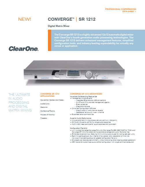
CONVERGE TM| SR 1212 Digital Matrix Mixer PROFESSIONAL CONFERENCINGDATA SHEET <THE ULTIMATE IN AUDIO PROCESSING AND DIGITAL MATRIX MIXING CONVERGE SR 1212APPLICATIONSConvention Centers and HotelsAuditoriumsStadiumsConference RoomsHouses of WorshipTheatersCONVERGE SR 1212 ADVANTAGESAdvanced Conferencing Feature Set+ Management Improvements> Integrated Ethernet and USB connections> SNMP and HTML remote management agents> Event scheduler> Diagnostic console+ Simplified Configuration Software> Drag & drop A/V and channel objects> Selectable views—unit, matrix, channel+ Expanded serial command setSuperior Audio Performance+ Unique automatic mixing process delivers optimum intelligibility+ 20 Hz-22 kHz bandwidth for full-range audio response+ ALC & AGC keep participants’ audio balanced and consistentConfiguration Flexibility+ Link multiple Converge/Converge Pro units (Converge Pro 880, 880T, 840T, 8i, TH20, andConverge SR 1212) for extensive microphone coverage and up to 16 phone lines+ Enhanced expansion bus, featuring 12 mix-minus audio buses for routing between units+ Eight mic gating groups (four internal & four global) allow separation of mics intoindividual mixer gating groups for greater configuration flexibility+ 32 presets can be executed on-the-fly without disturbing other ongoing preset operations+255 Macros for customized audio control/configuration with single command execution NEW!Audio PerformanceConditions: Unless otherwisespecified, all measurements areperformed with a 20 Hz to 22 kHzBW limit (no weighting)Frequency Response: 20 Hz to 22kHz ±1dBNoise (EIN): -126 dBu, 22 kHz BW,max gain,Rs=150 ΩTHD+N: <0.02%Dynamic Range: 100 dB (non A-weighted)Crosstalk <-91 dB re 20 dBu @ 20kHz channel to channelAuto Mixer ParametersNumber of Open Microphones (NOM) PA Adaptive ModeFirst Mic Priority ModeLast Mic ModeMaximum # of Mics ModeAmbient LevelGate Threshold AdjustOff Attenuation AdjustHold TimeDecay RateMatrix Mixing Parameters12 analog inputs/outputs12 expansion bus in/out8 assignable processing blocks in/out4 assignable fader blocks in/out Assignable Processing BlocksFiltersAll passLow passHigh passLow shelvingHigh shelvingParametric EQNotchCD HornCrossoversBesselButterworthLinkwitz-RileyCompressorDelay–adjustable up to 250 ms Assignable Fader BlocksGain/MuteMicrophone Input ConfigurationInput Gain AdjustMic or Line LevelPhantom Power on/offFiltersAll PassLow PassHigh PassNotchPEQMute on/offChairman Override on/offAGC on/offAutomatic Level Control on/offAuto Gate/Manual gateAdaptive Ambient on/offMic/Line Inputs 1-8Push-on mini-terminal block,balanced, bridgingImpedance: < 5 KΩNominal Level: adjustable -56 dBu to0 dBu (7 dB stepcoarse gain adjustment)Maximum Level: -65 dBu to +20 dBuLine Inputs 9-12Push-on mini-terminal block,balanced, bridgingImpedance: < 5 KΩNominal Level: 0 dBuMaximum Level: 20 dBuOutputs 1-12Push-on mini-terminal block, balancedImpedance: < 50 ΩNominal Level: 0 dBuMaximum Level: 20 dBuExpansion Bus In/OutProprietary NetworkRJ-45 (2), 1.9 MbpsCAT-5 twisted-pair cable, 200’maximum cable length between unitsEthernetAutoswitching with Quality ofConnection (QoC)10/100 Mbps Ethernet Network Port10/100 Mbps Ethernet PC PortRJ-45 ConnectorsRS-232Serial Command Protocol Only(Console software notsupported on RS- 232 port)DB-9 female9,600/19,200/38,400/57,600/115,200baud rate; 8 bits,1 stop bit, no parityHardware flow control on (default)/offControl/Status PortsDB-25 female A/B (2)Inputs A/B: active low (pull to ground)Outputs A/B: open collector, 40 VDCmax, 40 mA each+3.3 VDC pins (2) (300 mA over-current protected)USBVersion 2.0 compatibleT ype: B-connectorConfiguration & AdministrationSoftwareConverge™ ConsolePower Input RangeAuto-Adjusting100–240 VAC; 50/60 HzPower Consumption30 W T ypicalDimensions (L x D x H)17.25” x 10.25” x 1.75”43.8 x 26 x 4.5 cmWeight7.5 lbs/3.3375 kg unit weight12 lbs/5.4kg shipping weightOperating T emperature14° F/-10° C to 122° F/50° Cambient unit temperatureApprovalsSee the Installation & OperationManual for complete detailsAES48-2005: AES standard oninterconnections —Grounding and EMC practices— Shields of connectorsin audio equipment containingactive circuitry (self certified)Optional AccessoriesConverge Pro 880Converge Pro 880TConverge Pro 840TConverge Pro 8iConverge Pro TH20Tabletop ControllerPart Number910-151-900 Converge SR 121212x12 Digital Matrix MixerCONVERGE SR 1212 DATA SHEET <> CONVERGE SR 1212 BACK PANEL > SPECIFICATIONS> CLEARONE LOCATIONSHeadquarters:Salt Lake City, UT USA 5225 Wiley Post Way Suite 500Salt Lake City, UT 84116 Tel: 801-975-7200T oll Free: 800-945-7730 Fax: 801-977-0087******************Latin AmericaTel: 801-974-3621*******************EMEATel: 44 (0) 1189 036 053*******************APACTel: 801-303-3388*******************Other product names may be registered trademarks of their respective owners who do not necessarily endorse ClearOne or ClearOne’s products. All rights reserved. Information in this document subject to change without notice.© 2007 ClearOne Communications Inc. 802-151-900 Revision 1.1 January 2008.。
esp32_ 硬件设计指南说明书

ESP32硬件设计指南版本3.3乐鑫信息科技版权©2022关于本文档《ESP32硬件设计指南》主要提供了在使用ESP32系列产品进行电路设计和PCB布局时需注意的事项。
本文还简要介绍了ESP32系列产品的硬件信息,包括ESP32芯片、模组、开发板以及典型应用方案等。
文档版本请至乐鑫官网https:///zh-hans/support/download/documents下载最新版本文档。
修订历史请至文档最后页查看修订历史。
文档变更通知用户可以通过乐鑫官网订阅页面/zh-hans/subscribe订阅技术文档变更的电子邮件通知。
您需要更新订阅以接收有关新产品的文档通知。
证书下载用户可以通过乐鑫官网证书下载页面/zh-hans/certificates下载产品证书。
目录1产品概述12原理图设计2 2.1电源32.1.1数字电源32.1.2模拟电源52.1.3RTC电源5 2.2上电时序与复位62.2.1上电时序62.2.2复位6 2.3Flash(必选)及SRAM(可选)72.3.1SiP Flash及SiP PSRAM72.3.2外部Flash及片外RAM7 2.4时钟源72.4.1外部时钟参考(必选)82.4.2RTC时钟(可选)8 2.5射频(RF)9 2.6ADC9 2.7外置阻容10 2.8UART10 2.9SDIO11 2.10触摸传感器113版图布局12 3.1独立的ESP32模组的版图设计123.1.1版图设计通用要点123.1.2模组在底板上的位置摆放133.1.3电源143.1.4晶振163.1.5射频173.1.6Flash及PSRAM183.1.7外置阻容183.1.8UART183.1.9触摸传感器18 3.2ESP32作为从设备的版图设计20 3.3版图设计常见问题213.3.1为什么电源纹波并不大,但射频的TX性能很差?213.3.2为什么芯片发包时,电源纹波很小,但射频的TX性能不好?213.3.3为什么ESP32发包时,仪器测试到的power值比target power值要高很多或者低很多,且EVM比较差?213.3.4为什么芯片的TX性能没有问题,但RX的灵敏度不好?224开发硬件介绍235典型应用案例24 5.1ESP32智能音频平台245.1.1ESP32-LyraT音频开发板245.1.2ESP32-LyraTD-MSC音频开发板25 5.2ESP32触摸传感器方案—ESP32-Sense Kit26 5.3ESP-Mesh应用—ESP32-MeshKit27修订历史28插图1ESP32系列芯片参考设计原理图2 2四线3.3V内部flash核心电路图3 3VDD_SDIO电源管脚电路(1.8V)4 4VDD_SDIO电源管脚电路(3.3V)4 5VDD_SDIO电源管脚电路(外部电源供电)4 6ESP32系列芯片模拟电源5 7ESP32系列芯片RTC电源5 8ESP32芯片上电、复位时序图6 9ESP32晶振电路图8 10外置晶振电路图8 11外部激励信号电路图9 12ESP32射频匹配电路图9 13ESP32外置电容10 14ESP32串口11 15ESP32版图设计12 16ESP32模组在底板上的位置示意图13 17ESP32天线区域净空示意图14 18ESP32四层板电源设计15 19九宫格设计15 20ESP32两层板电源设计16 21ESP32晶振设计16 22ESP32四层板射频部分版图设计17 23ESP32两层板射频部分版图设计17 24ESP32Flash及PSRAM版图设计18 25ESP32UART设计18 26典型的触摸传感器应用19 27电极图形要求19 28传感器布局布线20 29PAD/TV Box平面位置规划框架20 30ESP32-LyraT俯视图24 31ESP32-LyraT仰视图25 32ESP32-LyraTD-MSC外观图26 33ESP32-Sense Kit开发套件26 34ESP32-MeshKit-Light灯27 35ESP32-MeshKit-Sense开发板271.产品概述ESP32是集成2.4GHz Wi-Fi和蓝牙双模的单芯片方案,采用台积电(TSMC)低功耗40纳米工艺,具有超高的射频性能、稳定性、通用性和可靠性,以及超低的功耗,满足不同的功耗需求,适用于各种应用场景。
HC-12 V2.6无线串口通信模块用户手册说明书
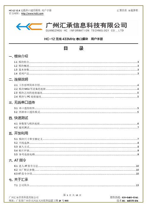
HC-12无线433MHz串口模块用户手册目录一.模块介绍1.1模块特点 (3)1.2模块概述 (3)1.3基本参数 (3)1.4系列产品 (3)二.连接说明2.1工作原理简单介绍 (4)2.2模块MCU等设备的连接 (4)2.3模块之间的连接通讯 (5)2.4模块与PC连接通讯 (5)三.无线串口透传3.1串口透传特性 (5)3.2四种串口透传模式 (5)四.快速测试4.1参数架与模块连接 (6)4.2通讯测试 (7)五.开发利用5.1模块尺寸和引脚定义 (7)5.2天线选择 (8)5.3嵌入方式 (8)5.4贴片炉温 (9)5.5参考连接电路 (9)六.AT指令6.1进入AT指令方法 (10)6.2出厂默认参数 (10)6.3AT指令介绍 (10)七.关于汇承7.1公司简介 (13)版本信息HC-12V2.6发布日期2018年07月11日修改记录1.增加FU2模式下发送数据时间间隔的说明。
(2013.10.17)2.修正应用实例及电路中HC-12模块与MCU串口连接的线路图。
(2013.12.26)3.FU3模式1200波特率恢复成和1.13版本的一样,同时增加FU4模式。
FU4模式下串口波特率固定为1200bps,空中波特率为500bps,可以提高通信距离。
该模式下,只适用传输少量数据(每个数据包在60个字节以内),数据包发送时间间隔不能太短(最好在2秒以上),否则会造成数据丢失。
(2014.09.18)4.修改了FU2模式下,只适用传输少量数据(每个数据包在20个字节以内),数据包发送时间间隔不能太短(最好在2秒以上),否则会造成数据丢失。
(2014.09.18)5.软件版本由原来的V2.3升级为V2.4。
(2016.12.02)6.软件版本由原来的V2.4升级为V2.6。
(2018.07.11)1.1模块特点※远距离无线传输(开阔地1000米/FU4模式下,空中波特率500bps)※工作频率范围(433.4—473.0MHz,多达100个通信频道)※最大100mW(20dBm)发射功率(可设置8档功率)※四种工作模式,适应不同应用场合※内置MCU,通过串口和外部设备进行通信※不限一次发送的字节个数(FU1/FU3模式)※模块支持一对一、一对多、多对多连接透传1.2模块概述HC-12无线串口通信模块是新一代的多通道嵌入式无线数传模块。
IR RECEIVER MODULE说明书
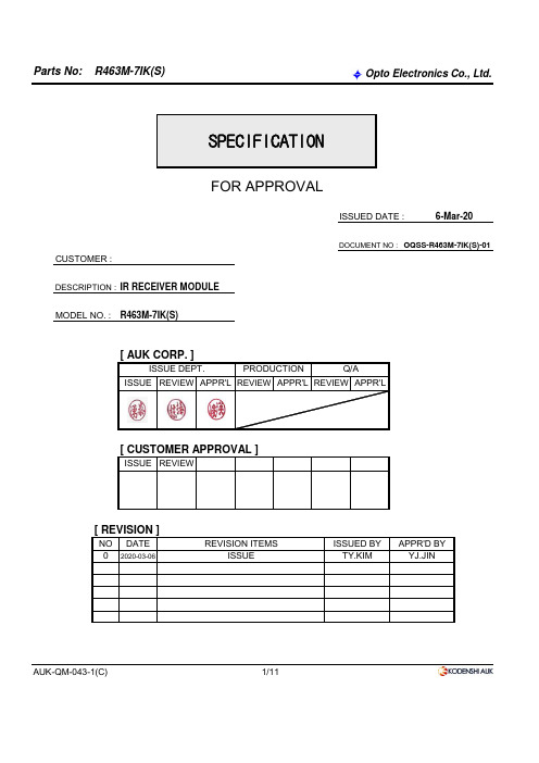
ISSUED DATE :CUSTOMER :IR RECEIVER MODULEMODEL NO. : R463M-7IK(S)[ AUK CORP. ][ CUSTOMER APPROVAL ][ REVISION ]AUK-QM-043-1(C)1/11DESCRIPTION :0NO PRODUCTIONREVIEW APPR'L DATEISSUE REVIEWQ/AYJ.JINISSUE DEPT.APPR'L2020-03-06ISSUE TY.KIM ISSUE REVIEW APPR'L REVIEW APPR'D BY ISSUED BY REVISION ITEMS6-Mar-20FOR APPROVALOQSS-R463M-7IK(S)-01DOCUMENT NO : SPECIFICATIONThis specification sheets include the contents under the copyright of AUK CORP.("AUK"). Please keep them with reasonable care as important information.Please don't reproduce or cause anyone reproduce them without AUK's consent.AUK takes no responsibility for damage caused by improper use of the devices which does not meet the conditions and absolute maximum ratings to be used specifiedin the relevant specification sheet.Please obey the instructions mentioned below for actual use of this device.① This device is designed for general electronic equipment.Main use of this device are as follows;* Computer * OA equipment * Telecommunication equipmet(Terminal)* Measuring instrument * Machine tool *Industrial robot* AV equipment * Home appliance,etc.② Please take proper steps in order to maintain reliability and safety, in case this device is used for the uses mentioned below which require high reliability.* Unit concerning control and safety of a vehicle (air plane,train,automobile etc.)* Traffic signal * Gas leak detection breaker* Fire box and burglar alarm box * Other safety equipment,etc.③ Please don't use for the uses mentioned below which require extremely high reliability.* Space equipment * Telecommunication equipment(Trunk)* Nuclear control equipment * Medical equipment(relating to any fatal element),etc. AUK-QM-043-2(C)2/111. DescriptionTheconsist of a PIN Photodiode of high speed and a preamplifier IC in the package as anreceiver for Infrared remote control systems2. Features◆ 2.7 ~ 5.5Volt supply voltage, low power consumption◆ Shielded against electrical field disturbance ◆ High immunity against ambient light ◆ Easy interface with the main board ◆ TTL and CMOS compatibility ◆ One mold package ◆ RoHS CompliancePinning:1 = GND,2 = Vcc,3 = Out3. Applications◆ TV, VTR, Audio, Air Conditioners, Car Stereo Units, Computers, Interior controlling appliances, and appliances that require remote controlling4. Package OutlinesSee the attached Drawing No.RM-R46□□-ASY-015. Absolute Maximum Ratings [Ta = 25℃ ]6. Reliability Test AUK-QM-043-2(C)3/11R463M-7IK(S)ParameterSymbolRatingT opr.260(Max 10 sec)T sol.Note : Storage Temperature T stg. Soldering TemperatureHeat Cycle *1 Dropping *2Supply Voltage / Output Voltage V cc 6 Supply Current / Output Current I out 2.5 Operating Temperature ℃Reflow Soldering Temperature (Pb Free)T sol.℃ Low Temperature *1 Moisture Sensitivity LevelsHigh Temperature / High Humidity *1Ta=+85℃, 85%RH, Vcc=5V t=240H Ta=-30℃, Vcc=5V t=240H Unit㎃℃-20℃∼80℃-25℃∼85℃℃hard wooden board from a 75㎝ height position(excepting deforms of terminals)V 260(Max 5 sec)ParameterHigh Temperature *1RatingTa=+80℃, Vcc=5V t=240H *1. Electro-optical Characteristics shall be satisfied after leaving 2hours in the normal temperature*2. Electro-optical Characteristics shall be satisfied and no deforms and destructions of appearance.Level 4 ( ≤30℃ / 60% RH 72hours )-25℃(0.5H) ∼+85℃(0.5H) 20cycleTest devices shall be dropped 3 time naturally onto 1237. Electro-optical Characteristics[ Ta= 25℃, Vcc=5.0V ]: 100 Ω ~ 470 Ω : 47 ㎌ ~ 100 ㎌: Optional (when using 10㏀ or more )When Rp is lower than 10㏀, Micom can't reply by a VoL rise.: Optional (when using 100 ㎊ less than)AUK-QM-043-2(C)4/11-: Indoor without extreme reflection of light400㎲under the conditions below against the standard transmitter Low Level Output Pulse Width *3-8000.5㎲400V OL -0.2Vcc-0.5Vcc-0.3High Level Output Pulse Width *3Note : *3. It specifies the maximum distance between emitter and detector that the output waveform satisfies the standard(8-2,3)T WLHigh Level Output Voltage *3-1) Measuring place 2) Ambient light source : Detecting surface illumination shall be irradiate 200±50Lux under ordinary white■ Cp1(Vcc-GND terminal series Condenser)■ Cp2(Vout-GND terminal pararllel Condenser)■ Rs (Vcc input series resistor)■ Rp (Vcc-Vout terminal Pullup resistor)4) Application Circuit : Recommend to design a circuit without using Rp & Cp2.fluorescence lamp without high frequency lightning3) Standard transmitter 1.6Vp-p under the measuring circuit specified in drawing(8-2,3) 200Lux0 ˚-I cc No InputSignalV cc =5V V cc =3VParameterSymbol 0.3λp Arrival Distance *3Peak Wavelength *3 Supply Voltage Range Unit- Current Consumption B.P.F Center Frequency f o ㎃㎚-37.9-㎑0.350.55V Min.Typ.Max.V cc 2.7 5.5ConditionsActive Low OutputV OH Low Level Output Voltage *3-800- Output FormBurst Wave = 600㎲Period = 1.2㎳V V T WH -±30 ˚m 32-m -4030cm over the ray axis : Burst wave indicated in drawing(8-1) of standard transmitter shall be arranged toL -940Receiver VccGNDVccGNDVout Cp1RsModuleMicomCp2TransmitterRp8. Measure Method8-1. Output Pulse Width8-2. Standard Transmitter+3.3V8-3. Test Condition of Transmission DistanceAUK-QM-043-2(C)5/11Transmitter output Carrier Frequency(fo)Duty50%Remocon output pulseT WLT WH600us 600usV OHV OL25Cm10㏀10㎌Vout10㏀TransmitterStandard TransmitterTransmission Distance : LVoutGND VCCOSC: Indicates horizontal and vertical directionsStandard θθθ9. Inspection CriteriaIn electro-optical characteristics, total quantity shall be inspected as below.- Front distance between emitter and detector - Current consumption - High level output voltage - Low level output voltage10. Customer must check below clauses before using10-1. When this infrared remote control detecting unit shall be adopted for wireless remote control, please keep the following standards.1) Data word length = Max. 100msec ●●●2) tpause = Min. 25msec ●××3) Duty(Σtburst /T ) = Max. 30%●×●4) tBurst = Min. 225usec ●×●5) tGap = Min. 330usec6) above (1)~(5) should be all meet and all remote control button should be operated properly.10-2. We recommand minimum 30cm distance between RC-M and transmitter for normal operating.If the distance between RC-M and Transmitter is too near, it might not respond. 10-3. If your condition doesn't meet the above statement, it might not operate properly.11. Caution(When use and storage of this device)AUK-QM-043-2(C)6/11RC5 / RC6SONY 15bit Mitsubishi Code Toshiba Micom CodeSONY 20bit Zenith Code 11-1. Store and use where there is no force causing transformation or change in quality11-2. Reflow maximum temperatuer is 250+0/-5℃ within max 10seconds within 72 hours From 30℃/60% humidity. during 96 hours which are a temperatre where has not become the damage of reel packing.11-3. From 30℃/60% humidity there is not the reflowing problem within 72 hours, but when the temperature11-4. Do not wash this device. Wipe the stains of diode side with a soft cloth.11-5. The shield case shall be grounded on the PCB pattern. There are two cases, one is that shield case If the receiver modules of shield case is not becoming ground connection, there is a possibility of being weakMatsushita Code in the EMI(Electronic Microwave Interperence) condition.Sharp CodeRCMMJVC CodeContinuous Data communication don't support. (tpause = 0ms)Suitable data format : ●Not recommend data format : xNEC CODE SONY 12bit condition is higher or 72 hours lapse after opening, product guideline is encouraged to dry from 60℃+5℃, ≤5% RHup to M.M 200V , HBM 2KV12. Period of Guarantee and Extent of Guarantee12-1. Period of Guarantee1 year after designated place.13. OthersAUK-QM-043-2(C)7/1111-10. This device has to control of static electricityObject : mercury, lead, cadmium, hexavalent chromium, polybrominated biphenyls and polybrominated diphenyl othersM.M = MACHINE MODEL(Resistance: 0KΩ Capacitor: 200pF)HBM = HUMAN BODY MODEL( Resistance: 1.5kΩ Capacitor: 100pF)In case where any trouble or questions arise, both parties agree to make full discussion covering the said problem11-7. Put decoupling device between Vcc and GND for reduce the noise from power supply line.11-8. The decrease in distance, the output noise, the malfunction, etc. might occur because of a surrounding 11-9. To prevent static electricity damage to the Pre-AMP make sure that the human body, the soldering iron is11-6. Solder pad within the condition of ratings. after soldering do not add extrorse force.connected to ground before usingrecommand Vcc-GND 47㎌ and Vcc- 100Ω. Decoupling device should be near receiver modules.R463M-7IK(S)12-2. Extent of GuaranteeKODENSHI AUK Corp. Shall supply the replacements against defects that will caused from KODENSHI AUK Corp. fault.12-3. This product complies with RoHS directive. electromagnetic environment.11-11. This device is not design to endure radiate rays and heavily charged particles.KODENSHIAUK Corp. guarantees a Receiver ModulesSOURCERC14. Reflow14-1. Regarding preheat and main heating, please set the temperature according to the reflow temperature profile as below.14-2. Even it is within the temperature profile condition as below, the disconnection of wire in the package might be caused by the stress join the package due to the PCB's curving and bending.Please take care about the condition of reflow machine when use.Recommended lead free reflow soldering temperature profile.14-3. Set the fumace temperatures for per-heating and heating in accorance with the reflow temperature profile as shown in the diagram.Exercise extreme care to keep the maximum temperature below 260℃.The temperature shown in the profile means the temperature at the device surface.Since there is a temperature difference between the component and the circuit board. It should be verified that the temperature of the device is accurately being measured.14-4. Please do not pile something on the product at reflow soldering because the transformation of the package resin may caused.14-5. When you do the reflow soldering twice, please process second reflow soldering within 8 hours after finish the first soldering14-6. Handing after reflow should be done only after the work surface has been cooled off.15. Manual Soldering15-1. Use a soldering iron of 25W or less. Adjust the temperature of the soldering iron below 350℃.15-2. Finish sodering within three seconds.15-3. Handle products only after the temperature has cooled off.15-4. To avoid the product is transformed and breakdown, it needs to take care that the power should not join to the product at soldering or immediately after soldering.AUK-QM-043-2(C)8/1116. DIMENSIONAUK-QM-043-2(C)9/1117. TAPING17-1. Taping specification・dimensions・product unsertion17-2. Reel specification・dimensionsMaterial : PS Conductivity The minimum packing quantity : 2,600pcs/reel AUK-QM-043-2(C)10/11Parts No : R463M-7IK(S)18. PACKINGAUK-QM-043-2(C)11/11Out Box Cardboard 450 x 450 x 36031,200 pcsITEM Size (W x L x H ㎜)Quantity MaterialsPlastic Reel 13" x 16Polystyren (Antistatic)2,600 pcs A.L Shieldng Bag400 x 450 x 0.2t Aluminum 2,600 pcs Opto Electronics Co., Ltd.IR Recevier_1pcs13Inch Reel = 2,600pcsLabelA.L Shielding BagLabelDry-Pack 50g*1eaMoisture-Sensitive DevicesLevel "4"Humidity Indication CardA.L Shielding Bag x 12ea(max)Out Box_OB-87Buffer Box_IB-87Buffer Box_IB-87Out Box_OB-87 =A.L Shielding Bag x 12ea + Buffer Box x 2eaA.L Shielding Bag x 12ea (max)TapingOut Box_OB-87 = 31,200pcsLabelxxxx-xxxxxxDG92xxxx-xxxxxxxxxxxxPART NO : .SPECIFICATION : R.MODULE[XX] LOT NO : 2A01-A1101 QTY : 31200VENDOR P/N : R463M-7IK(S) VENDOR/CODE : OEC / DG922012-01-11MSL 4RoHS。
蓝牙音频开发包Winbond W681360编解码器板用户手册说明书

Bluetooth Audio Development Pack Winbond W681360 Codec BoardUser GuidePart Number ACC-005The information contained in this document is subject to change without notice. EZURiO Ltd makes no warranty of any kind with regard to this material including, but not limited to, the implied warranties of merchant ability and fitness for a particular purpose. EZURiO Ltd shall not be liable for errors contained herein or for incidental or consequential damages in connection with the furnishing, performance, or use of this material.© Copyright 2006 EZURiO Limited. All rights reserved.No part of this document may be photocopied, reproduced, or translated to another language without the prior written consent of EZURiO.Other product or company names used in this publication are for identification purposes only and may be trademarks of their respective owners.Bluetooth® Development KitWinbond Audio Codec BoardPart Number: ACC-0051.General DescriptionThe EZURiO Winbond Codec Evaluation Board plugs into the EZURiO Developers kit and allows you to rapidly test and evaluate Bluetooth audio applications using the EZURiO Bluetooth Intelligent Serial Module to implement the wireless link.The ACC-005 evaluation board is based on the Winbond W681360 codec - a 3V, single channel, 13 bit linear voice-band codec, which is pin compatible to the Motorola MC145483. The codec is used to digitise incoming audio from the microphone into PCM data and convert the PCM digital audio output of the Bluetooth chip into an analogue signal for the headphones. The codec board has a microphone input and headphone output which are compatible with standard PC headsets.The W681630 codec has several features such as power down mode and high pass filter disable (to allow frequencies down to DC to be used). The ACC-005 codec evaluation board provides options to allow these features to be tested.The W681360 incorporates a feature that allows the volume of the codec output to be digitally controlled via 3 bits of the PCM data stream. The BISM II provides an AT command (ATS589) that allows you to control the volume of the codec.This document provides you with information to prototype and evaluate your own audio application. Once you have tried out your application, you will be able to design your own audio solution based around the Winbond codec and the EZURiO Bluetooth Intelligent Serial module.Bluetooth is a trademark owned by Bluetooth SIG, Inc., USA and licensed to EZURIO Ltd.2.OverviewThe codec board is powered by an on-board 3.3V regulator to reduce noise to a minimum. The PCM control signals for the codec go directly to the Bluetooth module on the motherboard via the 10-way connector, as do the 3 push button switches. This allows the switches to be used with an external program that implements the upper portion of headset or Handsfree profile.The microphone input, designed to interface to PC compatible headsets, has a fixed gain of 16 set by external components to the codec (the amplifier itself is part of the codec). Part of the microphone signal is mixed into the headphone output signal via VR2. This feature is known as “sidetone” and allows the user to hear their own voice when speaking. It is commonly used in telephony applications to give the user the necessary audio feedback that their ears expect.The audio output gain is by default fixed at 1. By fitting VR1, the audio gain can be made adjustable.The 120mW stereo output amplifier U3 ensures that the codec board can drive standard 32Ωstereo headphones while keeping total harmonic distortion down to 0.1%.Component PlacementNote that not allcomponents are fitted –non-fitted components areshown without pads. Referto Section 7 for details ofcomponent fitment andspecification.3.Codec Board Quick Start Guide3.1 Getting StartedThe codec board is supplied with a right angle, 10 way connector that can be used to connect it to the main developers kit. If required, this should be soldered to the main board. Alternatively other connectors or ribbon cables can be used.3.2 Equipment Required (not supplied)•Headsets (with microphone) (Standard PC headsets are fine)•EZURiO Wireless Developers Kit•BISM II Bluetooth module (Firmware release V9_20_22 onwards supports audio volume control)Normally two sets of development kit are required to test both ends of an audio link. If an application is being developed with an existing endpoint, such as a mobile phone or headset, only one set may be needed.3.3 Motherboard Jumper SettingsBefore using the codec board, there is a jumper setting on the motherboard that needs to be checked. This is CB1, next to the USB adaptor, which must be removed. If fitted it will short out the PCM output from the codec and prevent it operating. CB1 is only relevant for the WLAN 802.11 data module.3.4 Procedure:1)Plug the BISM II into the socket on the Dev Kit, connect to a PC serial port and power up.See the dev kit manual for different power supply options.2)Check that AT commands are working using EZURiO terminal. (Refer to blu2i Quick StartGuide if needed)3)Run the “ATI3” command to find out the firmware release number. If it is less thanV9_20_22, contact EZURiO to get a firmware upgrade for the BISM II. (Note: older versions of firmware will work, but audio output will be at half the full volume and the ats589=7 command will not be recognised)4)Power down, plug the codec board into the dev kit and power up. Check that ATcommands are working.Configure the Slave unit as follows:AT&F* Restore system defaultsATZ Reset the unit= 4 Makeconnectable and discoverableATS512ATS0=1 Answer after 1 ringATS531=1 Keep AT command mode going after a connection isestablishedATS589=7 Set Max. Volume level (requires firmware V9_20_22)AT&W Save the above settingsATZ Reset the unit.5) Find out the Bluetooth address of the Slave Unit by typing ATI4<return>6) Configure the Master Unit as follows:AT&F* Restore System DefaultsATZ Reset the unitATS531= 1 Keep the AT commands going after a connection isestablishedATS589=7 Set volume to maximumAT&W Save to flashATZ Reset the unit.ATD008098nnnnnn Connect to the slave (substitute your slave’s Bluetoothaddress that you found in step 5 for nnnnnn)AT+BTA1 Establish an audio link – displays AUDIO ON on both sides.(Alternatively AT+BTA7 can be used and the units willnegotiate the best link type.)An Audio link is now established between the two units.AT=BTA0 will turn off the audio link (but still leave the units connected).To change volume use ATS589. ATS589=0 gives minimum, ATS589=7 gives maximum. 4.Bluetooth SCO Links – A Primer4.1 Normal SCOBluetooth uses a Synchronous Connection-Orientated link (SCO) for audio. All this means is that for an audio link, the bandwidth needed to maintain the data rates required by the audio link is pre-allocated between the master and slave. This ensures audio data is always transmitted at the required data rate, and takes priority over the transmission of digital data.The Bluetooth specification for SCO is such that there is no re-transmission if data is corrupted or lost. This explains the crackling and popping that occurs when you get to the limits of radio range.The actual data rate over the air is 64 kbits/sec. There are 1600 timeslots available per second and when a master transmits a SCO packet in one timeslot, the slave replies with its SCO packet in the next. The SCO packet size is fixed at 240 bits (30 bytes). This means when a SCO link is established using the HV3 packet type, two out of every 6 timeslots are used up by the SCO link. This means there is enough bandwidth to have up to three SCO links active between a master and slave at the same time. In this scenario, there are no spare timeslots for other data.There are 3 main types of SCO packets, HV1, HV2 and HV3 (High Quality Voice). As mentioned earlier, the HV3 packet type has a 1 to 1 mapping between incoming audio data and the data transmitted over the air. There is no error correction possible with HV3.With HV1, each bit is transmitted 3 times and a simple voting algorithm is used at the other end to correct for any bit errors. This means that only 10 bytes of actual audio data can be transmitted in a SCO packet. To maintain the 64 kbits/sec data rate, all 6 timeslots have to be used for the SCO link, leaving no bandwidth available for data.With HV2, an FEC algorithm is used to correct for 1 bit errors. This increases the data packet size by 50%. This means that only 20 bytes of actual audio data can be transmitted in a SCO packet. To maintain the 64 kbits/sec data rate, 4 out of every 6 timeslots are used for the SCO link.AT+BTA1 enables HV3AT+BTA2 enables HV2AT+BTA4 enables HV1AT+BTA7 allows the link manager to negotiate which packet type to use, the default is HV14.2 Enhanced SCOEnhanced SCO or eSCO was implemented as part of the 1.2 Bluetooth Core Specification Release. The main driving factor was to improve audio quality. This has been achieved by: 1)including a CRC as part of the audio data packet to allow error detection and a re-transmission request. 2)allowing higher data rates by using packets that span more than 1 timeslot 3) allowing asymmetric links to allow high quality audio to be streamed in one direction.eSCO offers significantly better audio quality, but has to be configured at both ends of the link before a unit is enabled to accept incoming connections or enquiries.To try out eSCO, add the ATS584=1 command to the commands listed in the quick start section immediately after the AT&F* and ATZ commands.Both ends of the link must be configured for eSCO for the audio link to be established. If one end is set to eSCO and the other to SCO, you will get an “AUDIO FAIL” when the AT+BTA1 command is issued.The following are the packet types associated with the AT+BTA commands for eSCO.AT+BTA1 – EV3 packet. Up to 30 bytes + CRC. Uses up 1 timeslotAT+BTA2 – EV4 packet. Up to 120 bytes + CRC + 2/3 FEC. Up to 3 timeslotsAT+BTA4 – EV5 packet. Up to 180 bytes + CRC. Up to 3 timeslots. Currently Unsupported4.3 SCO / eSCO Transport DelaysThe following delays have been measured between incoming audio and audio output at the other end of a Bluetooth link.Normal SCO: AT+BTA1 7.84 ms AT+BTA2 9.24 ms AT+BTA4 10.8 msEnhanced SCO AT+BTA1 12.1 ms AT+BTA2 33.4 ms AT+BTA4 41.2 msAs can be seen, the additional error correction of eSCO comes with a transport delay penalty. This is because a buffer is needed to ensure that there is still data to output while waiting for a corrupted data packet to be re-transmitted.For AT+BTA1 and normal SCO, the data is transmitted once every 6 timeslots so the transport delay is expected to be 6/1600 = 3.75ms. When doing loop-round testing with the codec, i.e. with no transport delay, it was found that from input to output, the codec added ~1ms of delay at 1kHz and 1.5ms at lower frequencies.4.4 PCM TimingThe codec samples at 8 kHz. The default mode of operation of the codec is 16 bit Receive Gain Adjust Mode. In this mode, in every 8 kHz cycle, 16 bits of data is clocked into the codec. The first 13 bits are PCM audio data, the last 3 bits are volume data. Of the last three bits, 000 equates to maximum volume (ATS589=7), 111 equates to minimum volume (Ats589=0).At maximum volume, the output signal matches the amplitude of the input signal at the other end of the Bluetooth link. It is more appropriate to think of this feature as being an attenuation control.The clock rate used for sampling is 250kHz (4µs). 16 clock cycles takes 64µs. 8kHz equates to 125µs.The same timing is used for all packet types in both SCO and eSCO modes.5.Frequency Response5.1 Codec Frequency ResponseThe codec frequency response can be measured by connecting PCM_IN from the codec to PCM_OUT to the codec (PCM_OUT from J1, the 10 way connector has to be disconnected). A 1kΩ pull down resistor is needed on PCM_OUT to ensure maximum volume setting.The following graph shows the measured frequency response. For this test, R32, the side-tone resistor was removed to prevent audio feedback.A 1V peak to peak sine wave was injected into the microphone circuit and its amplitude measured at TP5, A0, the input to the codec. The output from the codec was measured on TP6, PA0+.The chart below shows the codec frequency response with the High Pass Filter Enable (HB – Pin 16) pin set high and set low.As can be seen from the chart, the codec frequency response is flat between 300 and 3,300 Hz. With the high pass filter on, the 3dB points are at 150Hz and 3,600 Hz respectively. With the high pass filter off, the 3dB point goes down to approximately 15Hz.5.2 Bluetooth Link Frequency ResponseThe Codec 13bit linear data is coded within the Bluetooth chip using CVSD (Continuous Variable Slope Decode) encoding for transport over the Bluetooth link. CVSD is essentially a form of Adaptive Differential PCM (ADPCM) and is well suited for voice transmission. It is forgiving of individual bit corruption as each bit only implements an up or a down shift relative to the previous level (corruption of the MSB of a 13 bit sample would create a much larger error term than is possible with ADPCM). A draw back of ADPCM is that it cannot track large delta changes in signal quickly enough. For voice, this does not present a problem.The chart below shows the frequency response of the Bluetooth link at different levels of input sine wave.As can be seen, the frequency response can only be considered to be flat when the input voltage level is less than a 0.3V peak to peak sine wave.6.Circuit DescriptionThis section describes the individual parts of the circuit and give design information aboutthe components, to allow you to adapt the circuitry of the codec board for your own implementation.6.1 Audio AmplifierThe Winbond codec is capable of driving a 32Ω load directly if the gain of the output amplifier is reduced by a factor of 4. This is done by Setting R1 to 39kΩ.Of the stereo headsets tested, it was found that 32Ω was a common impedance for each earpiece. For a stereo headset where two speakers are being driven in parallel this would be equivalent to driving a 16Ω load. This is out of the codec’s specification so a small headphone amplifier, U3, has been used on the evaluation board. This is not required if the impedance of the earpiece is equal or greater than 32Ω.The large 100 μF decoupling capacitors have been used so that the codec could be tested in its “high pass filter mode disabled” configuration. If you do not require a frequency response to go down below 300 Hz, then these capacitors can be reduced to small values. The main design consideration is the impedance should not be significant compared to the impedance of the headphone selected at frequencies of interest.E.g. if using a 32Ω headphone and expecting a 3dB point at 300 Hz, then the decoupling capacitor impedance could be 32Ω at 300Hz i.e. 10 μF. This requires a much smaller footprint than the 100μF used in the reference design.6.2 Driving the Headset Directly from the CodecThis will achieve the most cost effective design but care must be taken to ensure that the 32Ω specification of load is met by selecting an appropriate headset.Remove R10, R13 and R12. Fit R11, R9, R38 as zero ohm links. Fit 39kΩ in place of R1 to reduce the gain by 4.In-house testing showed that with a 32Ω load and with R1 set to 39kΩ, that there was some distortion at zero cross-over but that it was not easily perceptible.Even though the output signal level had been reduced by a factor of 4, on the headsets tested, the volume levels sounded loud enough for most applications. It is important to check this with the target headset for your application.6.3 Microphone CircuitThe microphone circuit is designed for an electret microphone (which is commonly used in PC applications). Typically this would be powered by 5V via a 2.2kΩ series resistor. In the reference design, it is powered by 3.3V to ensure a clean supply regardless of the power supply used to power the Dev kit. This reduces the sensitivity of the microphone - you should test your application with the microphone and voltage you intend to use in order to determine your component values.The gain of the microphone is set by R22 and R24, with gain being equal to R22/R24. The current values are 62K and 3.9K, giving a gain of approximately 16. When changing to a different gain, R27 and R25 should be set to the new values as well. This ensures that the load seen by common mode noise on the microphone is identical and prevents it from being amplified.R31 is a no fit resistor. It’s purpose is to facilitate test modes where a user wants to loop audio output directly back to the audio input to conduct an over the air audio test.6.4 SidetoneWhen we talk, we hear our own voice, which is part of normal speech perception. If our ears are covered by headphones, we do not hear our voice, which is perceived as abnormal. (Try covering your ears while talking to notice the difference).To compensate for the loss in feedback to the ear when it is covered with a headphone, most telephony systems inject some of the microphone signal back into the audio output path so that the person perceives their own speech as normal. This feature is commonly referred to as sidetone.Variable resistor VR2 allows you to control the amount of sidetone that is fed back to the audio output so that the user perceives their speech as normal.If the headset design does not totally cover the ear, then the sideband circuitry can be omitted.6.5 Power DownFor battery powered audio applications, the power down feature of the codec allows you to turn it off and save power when it is not being used. This feature can be tested by fitting R7 with a 0Ωlink and controlling the PUI input of the codec via MPIO_5.For AT commands, MPIO_5 translates to GPIO 7.The put GPIO 7 into output mode, use “ats610=$040”To turn the codec on, use “ats627=1”To turn the codec off, use “ats627=0”6.6 Alternative PCM_CLKSome applications require that the PCM Clock is driven by external circuitry. This requires the PCM Interface provided by the BISM to be put in Slave mode and a clock is supplied by the external circuitry on MPIO_7.Contact Ezurio for further details if this is a requirement.6.7 SwitchesThe switches S1, S2 and S3 have no defined function. They are there to assist you to prototype your audio application. e.g. If your application requires a button to be pressed for the user to answer an incoming connection, you can prototype that function using one of the switches provided.ATS620 allows you to read the status of the GPIO ports.No switches pressed: ATS620? => $0028S1 pressed (GPIO 9) ATS620? => $0128S2 pressed (GPIO 7) ATS620? => $0068S3 pressed (GPIO 8) ATS620? => $00A86.8 High Pass Filter EnableThe W681360 can have its High Pass filter enabled or disabled, depending on the state of the HB pin (Pin 16). This is pulled high or low by R3 or R4 (Default). See section 5.1 for more details.6.9 GPIO to MPIO MappingAT commands use GPIO numbers to represent I/O lines. These GPIO numbers map to physical signals drawn on the schematics as MPIO lines. Some of the GPIO/MPIO lines are used when providing a full RS232 interface.The following tables gives the mapping between GPIO, MPIO and RS232 signals.DCD MPIO_3RI MPIO_2DTR MPIO_9DSR MPIO_8GPIO_1 MPIO_0GPIO_2 MPIO_1GPIO_3 MPIO_9GPIO_4 MPIO_10GPIO_5 MPIO_11GPIO_6 MPIO_4GPIO_7 MPIO_5GPIO_8 MPIO_6GPIO_9 MPIO_7Note: For the BISM PA (Class 1 design), MPIO_0 and MPIO_1 are used to control the RF switch so are not available to the AT Command Set.7. Bill of MaterialsNot all components are fitted, as some provide alternative functionality or implement non-standard options.Refer to the previous sections and the schematic for information on the component function. Components marked in blue are not fitted.Reference Part ToleranceDescription Manufacture r Part No / FootprintC1,C7100nF20%Ceramic Capacitor0805 C2,C3,C6 10uF '+80/-20% Tantalum Capacitor TANA C4,C5,C810nF20%Ceramic Capacitor0805C9,C10 100uF 20% Electrolytic Capacitor Panasonic EEE0JA101SP C11,C12,C17,C18 2.2uF '+80/-20% Ceramic Capacitor 0805 C13 22uF '+80/-20% Ceramic Capacitor 1210 C14 100nF '+80/-20% Ceramic Capacitor 0805 C15,C19 100pF 20% Ceramic Capacitor 0805 C161.0uF'+80/-20%Ceramic Capacitor0805D1,D2,D3,D4,D5,D6,D7,D8 BAT54S Dual Schottky Diode BAT54S Zetex BAT54S J1 10 Way 0.1" R/A PCB Socket Harwin M20-7891046 J2,J3 3.5mm 3way Audio Jack Skt Schurter 4832.232L110uHThin Film Inductor1210 R1,R2,R5,R35,R36,R37 10K 1% Thick Film Resistor 0805 R3,R7,R8,R9,R11,R34,R38 0R Not Fitted 5% Thick Film Resistor 0805 R4,R6,R10,R12,R13,R330R5%Thick Film Resistor0805 R14,R28,R29,R30 1K 5% Thick Film Resistor 0805 R152K2 Not Fitted 5% Thick Film Resistor 0805 R16,R17,R18,R19,R24,R25 3.9K 1% Thick Film Resistor 0805 R26,R20 1.5K 5% Thick Film Resistor 0805 R23,R21 200K 5% Thick Film Resistor 0805 R27,R22 62K1% Thick Film Resistor 0805 R31 62K Not Fitted 1% Thick Film Resistor 0805 R32 75K5% Thick Film Resistor0805 S1,S2,S3OMRON/B3S-1000Push Button Switch SPNO SMD Omron B3S-1000U1 AME8800AEFT 3.3V Low Drop Out Regulator300mA AME AME8800AEFT U2 W681360RG W681360RG CODEC Winbond W681360RG U3 LM4908MM Dual Headphone Amplifier Nat. Semi. LM4909MMVR1 20K Not Fitted 20% 20K Trimmer Vishay TS53YL 20K 20% TR VR250K20%50K TrimmerVishayTS53YL 50K 20% TR8. References1. Winbond W681360 Data Sheet – /PDF/Sheet/W681360.pdf2. ACC-005 Schematic – ERBLU49-002A1-029.DisclaimersEZURIO’S WIRELESS PRODUCTS ARE NOT AUTHORISED FOR USE AS CRITICAL COMPONENTS IN LIFE SUPPORT DEVICES OR SYSTEMS WITHOUT THE EXPRESS WRITTEN APPROVAL OF THE MANAGING DIRECTOR OF EZURIO LTD.The definitions used herein are:a) Life support devices or systems are devices which (1) are intended for surgical implant into the body, or (2) support or sustain life and whose failure to perform when properly used in accordance with the instructions for use provided in the labelling can reasonably be expected to result in a significant injury to the user.b) A critical component is any component of a life support device or system whose failure to perform can be reasonably expected to cause the failure of the life support device or system, or to affect its safety or effectiveness.EZURiO does not assume responsibility for use of any of the circuitry described, no circuit patent licenses are implied and EZURiO reserves the right at any time to change without notice said circuitry and specifications.9.1 Data Sheet StatusThis data sheet contains preliminary data for use with Engineering Samples. Supplementary data will be published at a later date. EZURiO Ltd reserve the right to change the specification without prior notice in order to improve the design and supply the best possible product.Please check with EZURiO Ltd for the most recent data before initiating orcompleting a design. Designers should check the production status of any engineering firmware used during development before it is deployed.。
ET11AR蓝牙双模模组_BT2.0+BT4.2_Module_Datasheet
ET11AR 蓝牙模块❖遵循Bluetooth 3.0/2.1+EDR与4.1/4.2(BLE)/BT5.0规范❖Arduino创客智能机器人小车专用双模蓝牙模块技术手册修改记录:2018.12.11 V1.0●First Release.2019.6.25 V2.0●更新统一固件版本,AT指令表添加AT指令. 2019.7.15 V3.0●更新模块实物图片.一.概述ET11AR是深圳市易联易通科技有限公司专为Arduino创客STEAM教育市场打造的双模蓝牙模块,遵循BT2.1+EDR/3.0/4.2(4.2-BR/EDR/BLE)BT5.0蓝牙规范,支持SPP和BLE双模模式。
模块支持直接对接arduino产品MCU端,实现蓝牙数传和蓝牙无线下载。
ET11AR模块集成以ARM® Cortex™-M3 为核心的赛普拉斯@CYPRESS(原美国博通@Broadcom)蓝牙4.2 LE+BR/EDR双模模块,集成蓝牙协议基带、MCU(Cortex-M3)、高增益射频PCB天线,采用工业级设计、ROHS制程,具有集成度极高、低功耗、蓝牙无线射频性能卓越等特点。
二.特点※支持连接PC蓝牙,无线下载烧录和数传控制。
※接口电平为3.3V~5.5V,可接各种单片机(Arduino,51,AVR,STC,PIC,ARM,MSP430等)※标准2.54排针接口,即插即用※与Arduino开发板串口并存,即蓝牙在线时,有线可以下载升级程序。
※主从一体,可以记忆识别连接上一次配对过的设备。
※自适应跳频技术,高性能无线收发系统,在空旷地带,收发距离可以达到20~80米※低功耗工作模式电流<20ma,高速传输上下行速度最大75KB/S.※支持空中升级(OTA)固件,解决客户的后顾之忧※支持配合客户需求,量身定制专属软件※标准HCI端口(UART)※模块自带串口排针设计,ROHS制程,BQB认证。
※模块完全集成了XTAL等外围元器件,设计简单,成本低※内置2.4G PCB天线,用户无需天线调试※简单易用,适用于串口近距离透传无线替代方案,无需理解蓝牙协议的具体开发※完善的技术支持,可提供APP开发等三.应用领域该模块主要用于短距离的数据无线传输领域,可以方便地和PC机、智能手机等无线终端上的蓝牙设备相连,也可以实现两个模块之间的数据互通,避免繁琐的线缆连接和空间限制,可以直接替代串口线。
MGM13S12 Module Radio Board BRD4305E 参考手册说明书
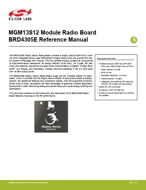
MGM13S12 Module Radio Board BRD4305E Reference ManualThe BRD4305E Mighty Gecko Radio Board contains a Mighty Gecko MGM13S12 mod-ule which integrates Silicon Labs' EFR32MG13 Mighty Gecko SoC into a small form fac-tor System-in-Package (SiP) module. The fully certified module contains all components (a high-performance transceiver, an energy efficient 32-bit MCU, HF crystal, RF pas-sives, and antenna) required for a system-level implementation of Zigbee, Thread, Blue-tooth®Low Energy, and proprietary wireless networks operating in the 2.4 GHz band with 18 dBm output power.RADIO BOARD FEATURES•Wireless Module: MGM13S12F512GA•CPU core: ARM Cortex®-M4 with FPU •Flash memory: 512 kB•RAM: 64 kB•Operation frequency: 2.4 GHz•Transmit power: 18 dBm•Integrated chip antenna, RF matchingnetwork, HF crystal, and decoupling •Option for UFL connector•Crystal for LFXO: 32.768 kHz•8 Mbit low-power serial flash for over-the-air updatesThe BRD4305E Mighty Gecko Radio Board plugs into the Wireless Starter Kit Main-board, which is included with the Mighty Gecko Starter Kit and gives access to display,buttons, and additional features from expansion boards. With the supporting SimplicityStudio suite of tools, developers can take advantage of graphical wireless applicationdevelopment, mesh networking debug and packet trace, and visual energy profiling andoptimization.This document contains a brief introduction and description of the BRD4305E RadioBoard features, focusing on the RF performance.Rev. 1.0Table of Contents1. Introduction (3)2. Radio Board Connector (4)2.1 Introduction (4)2.2 Radio Board Connector Pin Associations (4)3. Radio Board Block Summary (5)3.1 Introduction (5)3.2 Radio Board Block Diagram (5)3.3 Radio Board Block Description (5)3.3.1 Wireless SiP (5)3.3.2 LF Crystal Oscillator (LFXO) (5)3.3.3 UFL Connector (5)3.3.4 Radio Board Connectors (6)3.3.5 Serial Flash (6)3.3.6 Serial EEPROM (6)4. Mechanical Details (7)5. EMC Compliance (8)5.1 Introduction (8)5.2 EMC Regulations for 2.4 GHz (8)5.2.1 ETSI EN 300-328 Emission Limits for the 2400-2483.5 MHz Band (8)5.2.2 FCC15.247 Emission Limits for the 2400-2483.5 MHz Band (8)5.2.3 Applied Emission Limits for the 2.4 GHz Band (8)6. RF Performance (9)6.1 Conducted Power Measurements (9)6.1.1 Conducted Measurements in the 2.4 GHz Band (9)6.2 Radiated Power Measurements (10)6.2.1 Radiated Measurements in the 2.4 GHz Band (10)7. EMC Compliance Recommendations (11)7.1 Recommendations for 2.4 GHz ETSI EN 300-328 Compliance (11)7.2 Recommendations for 2.4 GHz FCC 15.247 Compliance (11)8. Board Revision History (12)9. Errata (13)10. Document Revision History (14)Introduction 1. IntroductionThe BRD4305E Radio Boards provide a development platform (together with the Wireless Starter Kit Mainboard) for the Silicon Labs Mighty Gecko MGM13S12 modules.By carrying the MGM13S12 module, the BRD4305E Radio Board is designed to operate in the 2400-2483.5 MHz with the maximum of 18 dBm output power.To develop and/or evaluate the MGM13S12 module, the BRD4305E Radio Board can be connected to the Wireless Starter Kit Main-board to get access to display, buttons, and additional features from expansion boards (EXP boards).2. Radio Board Connector2.1 IntroductionThe board-to-board connector scheme allows access to all MGM13S12 GPIO pins as well as the RESETn signal. For more information on the functions of the available pins, see the MGM13S12 data sheet.2.2 Radio Board Connector Pin AssociationsThe figure below shows the mapping between the connector and the MGM13S12 pins and their function on the Wireless Starter Kit Mainboard.GNDF9 / PA3 / VCOM.#RTS_#CS 3v3UIF_BUTTON1 / PF7 / P36P200Upper RowNC / P38NC / P40NC / P42NC / P44DEBUG.TMS_SWDIO / PF1 / F0DISP_ENABLE / PD15 / F14UIF_BUTTON0 / PF6 / F12UIF_LED0 / PF4 / F10VCOM.#CTS_SCLK / PA2 / F8DEBUG.RESET / RADIO_#RESET / F4DEBUG.TDO_SWO / PF2 / F2DISP_SI / PC6 / F16VCOM.TX_MOSI / PA0 / F6PTI.DATA / PB12 / F20DISP_EXTCOMIN / PD13 / F18USB_VBUS 5V Board ID SCL GNDBoard ID SDAUSB_VREG F7 / PA1 / VCOM.RX_MISO F5 / PA5 / VCOM_ENABLE F3 / PF3 / DEBUG.TDIF1 / PF0 / DEBUG.TCK_SWCLK P45 / NCP43 / NC P41 / NC P39 / NC P37 / PD9 / SENSOR_ENABLE F11 / PF5 / UIF_LED1F13 / PF7 / UIF_BUTTON1F15 / PC8 / DISP_SCLK F17 / PD14 / DISP_SCS F19 / PB13 / PTI.SYNC F21 / PB11 / PTI.CLK GNDVMCU_IN VCOM.#CTS_SCLK / PA2 / P0P201Lower RowVCOM.#RTS_#CS / PA3 / P2PD10 / P4PD11 / P6GNDVRF_INP35 / PD15 / DISP_ENABLEP7 / PC9P5 / PC8 / DISP_SCLK P3 / PC7P1 / PC6 / DISP_SI P33 / PD14 / DISP_SCSP31 / PD13 / DISP_EXTCOMINP29 / NCP27 / 1V8*P25 / NCP23 / NCP21 / NCP19 / NC P17 / NC P15 / NC P13 / PC11P11 / PA1 / VCOM.RX_MISO P9 / PA0 / VCOM.TX_MOSI UIF_BUTTON0 / PF6 / P34UIF_LED1 / PF5 / P32UIF_LED0 / PF4 / P30DEBUG.TDO_SWO / PF2 / P28DEBUG.TMS_SWDIO / PF1 / P26DEBUG.TCK_SWCLK / PF0 / P24PTI.SYNC / PB13 / P22PTI.DATA / PB12 / P20PTI.CLK / PB11 / P18VCOM_ENABLE / PA5 / P16PA4 / P14PC10 / P12DEBUG.TDI / PF3 / P10PD12 / P8* Connection is available by mounting the corresponding 0 Ohm resistor.(See the schematic of the Radio Board for details.)Figure 2.1. BRD4305E Radio Board Connector Pin MappingRadio Board Connector3. Radio Board Block Summary3.1 IntroductionThis section gives a short introduction to the blocks of the BRD4305E Radio Board.3.2 Radio Board Block DiagramThe block diagram of the BRD4305E Radio Board is shown in the figure below.Figure 3.1. BRD4305E Block Diagram3.3 Radio Board Block Description3.3.1 Wireless SiPThe BRD4305E Mighty Gecko Radio Board incorporates an MGM13S12F512GA Mighty Gecko MGM13S12 module featuring 32-bit Cortex®-M4 with FPU core, 512 kB of flash memory, 64 kB of RAM and a 2.4 GHz band transceiver with output power up to 18 dBm. For additional information on the MGM13S12F512GA, refer to the MGM13S data sheet.3.3.2 LF Crystal Oscillator (LFXO)The BRD4305E Radio Board has a 32.768 kHz crystal mounted. For details regarding the crystal configuration, refer to Application Note "AN0016.1: Oscillator Design Considerations".3.3.3 UFL ConnectorTo be able to perform conducted measurements, Silicon Labs added a UFL connector to the Radio Board. The connector allows an external 50 Ohm cable or antenna to be connected during design verification or testing.Note: By default, the output of the matching network is connected to the printed inverted-F antenna by a series component. It can be connected to the UFL connector as well through a series 0 Ohm resistor, which is not mounted by default. For conducted measure-ments through the UFL connector, the series component to the antenna should be removed and the 0 Ohm resistor should be mounted (see section for further details).| Building a more connected world.Rev. 1.0 | 53.3.4 Radio Board ConnectorsTwo dual-row, 0.05” pitch polarized connectors make up the BRD4305E Radio Board interface to the Wireless Starter Kit Mainboard. For more information on the pin mapping between the MGM13S12F512GA and the Radio Board Connector, refer to section 2.2 Radio Board Connector Pin Associations.3.3.5 Serial FlashThe BRD4305E Radio Board is equipped with an 8 Mbit Macronix MX25R SPI flash that is connected directly to the MGM13S12 to support over-the-air (OTA) updates. For additional information on the pin mapping see the BRD4305E schematic.3.3.6 Serial EEPROMThe BRD4305E Radio Board is equipped with a serial I2C EEPROM for board identification and to store additional board related infor-mation.4. Mechanical DetailsThe BRD4305E Radio Board is illustrated in the figures below.40 mmFigure 4.1. BRD4305E Top View24 mm20 mmFigure 4.2. BRD4305E Bottom ViewMechanical DetailsRev. 1.0 | 7EMC Compliance 5. EMC Compliance5.1 IntroductionCompliance of the fundamental and harmonic levels of the BRD4305E Radio Board is tested against the following standards:• 2.4 GHz:•ETSI EN 300-328•FCC 15.2475.2 EMC Regulations for 2.4 GHz5.2.1 ETSI EN 300-328 Emission Limits for the 2400-2483.5 MHz BandBased on ETSI EN 300-328, the allowed maximum fundamental power for the 2400-2483.5 MHz band is 20 dBm EIRP. For the unwan-ted emissions in the 1 GHz to 12.75 GHz domain, the specific limit is -30 dBm EIRP.5.2.2 FCC15.247 Emission Limits for the 2400-2483.5 MHz BandFCC 15.247 allows conducted output power up to 1 Watt (30 dBm) in the 2400-2483.5 MHz band. For spurious emissions the limit is -20 dBc based on either conducted or radiated measurement, if the emission is not in a restricted band. The restricted bands are speci-fied in FCC 15.205. In these bands the spurious emission levels must meet the levels set out in FCC 15.209. In the range from 960 MHz to the frequency of the 5th harmonic, it is defined as 0.5 mV/m at 3 m distance which equals to -41.2 dBm in EIRP.Additionally, for spurious frequencies above 1 GHz, FCC 15.35 allows duty-cycle relaxation to the regulatory limits. For the EmberZNet PRO the relaxation is 3.6 dB. Therefore, the -41.2 dBm limit can be modified to -37.6 dBm.If operating in the 2400-2483.5 MHz band, the 2nd, 3rd, and 5th harmonics can fall into restricted bands. As a result, for those harmon-ics the -37.6 dBm limit should be applied. For the 4th harmonic the -20 dBc limit should be applied.5.2.3 Applied Emission Limits for the 2.4 GHz BandThe above ETSI limits are applied both for conducted and radiated measurements.The FCC restricted band limits are radiated limits only. In addition, Silicon Labs applies the same restrictions to the conducted spec-trum. By doing so, compliance with the radiated limits can be estimated based on the conducted measurement, by assuming the use of an antenna with 0 dB gain at the fundamental and the harmonic frequencies.The overall applied limits are shown in the table below.Table 5.1. Applied Limits for Spurious Emissions for the 2.4 GHz Band | Building a more connected world.Rev. 1.0 | 86. RF Performance6.1 Conducted Power MeasurementsDuring measurements, the BRD4305E Radio Board was attached to a Wireless Starter Kit Mainboard which was supplied by USB. The voltage supply for the Radio Board was 3.3 V.6.1.1 Conducted Measurements in the 2.4 GHz BandThe BRD4305E Radio Board was connected directly to a Spectrum Analyzer through its UFL connector (the was removed and a 0 Ohm resistor was soldered to the position). The supply for the module (VDD) was 3.3 V provided by the mainboard; for details, see the sche-matic of the BRD4305E. The transceiver was operated in continuous carrier transmission mode. The output power of the radio was set to 18 dBm.The typical output spectrum is shown in the following figure.Figure 6.1. Typical Output Spectrum of the BRD4305EAs shown in the figure, the fundamental is just a bit under 18 dBm and all of the unwanted emissions are under the -37.6 dBm applied limit.Note: The conducted measurement is performed by connecting the on-board UFL connector to a Spectrum Analyzer through an SMA Conversion Adapter (P/N: HRMJ-U.FLP(40)). This connection itself introduces approximately 0.3 dB insertion loss.Rev. 1.0 | 96.2 Radiated Power MeasurementsDuring measurements, the BRD4305E Radio Board was attached to a Wireless Starter Kit Mainboard which was supplied by USB. The voltage supply for the Radio Board was 3.3 V. The radiated power was measured in an antenna chamber by rotating the board 360 de-grees with horizontal and vertical reference antenna polarizations in the XY, XZ, and YZ cuts. The measurement planes are illustrated in the figure below.Figure 6.2. Illustration of Reference Planes with a Radio Board Plugged into the Wireless Starter Kit Mainboard Note: The radiated measurement results presented in this document were recorded in an unlicensed antenna chamber. Also, the radi-ated power levels may change depending on the actual application (PCB size, used antenna, and so on). Therefore, the absolute levels and margins of the final application are recommended to be verified in a licensed EMC testhouse.6.2.1 Radiated Measurements in the 2.4 GHz BandThe supply for the module (VDD) was 3.3 V provided by the mainboard; for details, see the BRD4305E schematic. The transceiver was operated in continuous carrier transmission mode. The output power of the radio was set to 18 dBm based on the conducted measure-ment.The fundamental was set to the frequency where the maximum antenna gain was measured. The results are shown in the table below. Note: The frequency in which the antenna gain has its maximum value can vary between modules due to the technological spreading of the passive RF components and the antenna.Table 6.1. Maximums of the Measured Radiated Powers in EIRP [dBm]As shown in the table, the level of the fundamental is 17 dBm. The strongest harmonic is the double-frequency one and it is compliant with the -37.6 dBm applied limit with 0.7 dB margin. | Building a more connected world.Rev. 1.0 | 10EMC Compliance Recommendations 7. EMC Compliance Recommendations7.1 Recommendations for 2.4 GHz ETSI EN 300-328 ComplianceAs shown in the previous section, the power of the fundamental frequency of the BRD4305E Mighty Gecko Radio Board with 18 dBm output is compliant with the 20 dBm limit of the ETSI EN 300-328 regulation in both the conducted and radiated measurements. The harmonic emissions are under the -30 dBm limit with large margin.7.2 Recommendations for 2.4 GHz FCC 15.247 ComplianceAs shown in the previous section, the power of the fundamental frequency of the BRD4305E Mighty Gecko Radio Board with 18 dBm output is compliant with the 30 dBm limit of the FCC 15.247 regulation. The harmonic emissions are under the -37.6 dBm applied limit.Board Revision History 8. Board Revision HistoryTable 8.1. BRD4305E Radio Board RevisionsNote: The silkscreen marking on the board (e.g. PCBxxxx A00) denotes the revision of the PCB. The revision of the actual Radio Board is laser printed in the "Board Info" field on the PCB. Also, it can be read from the on-board EEPROM. | Building a more connected world.Rev. 1.0 | 12Errata 9. ErrataThere are no known errata at present.Document Revision History 10. Document Revision HistoryRevision 1.00July, 2018•Initial document revision. Silicon Laboratories Inc.400 West Cesar Chavez Austin, TX 78701USASimplicity StudioOne-click access to MCU andwireless tools, documentation,software, source code libraries &more. Available for Windows,Mac and Linux!IoT Portfolio /IoT SW/HW /simplicity Quality /quality Support and CommunityDisclaimer Silicon Labs intends to provide customers with the latest, accurate, and in-depth documentation of all peripherals and modules available for system and software implementers using or intending to use the Silicon Labs products. Characterization data, available modules and peripherals, memory sizes and memory addresses refer to each specific device, and "Typical" parameters provided can and do vary in different applications. Application examples described herein are for illustrative purposes only. Silicon Labs reserves the right to make changes without further notice and limitation to product information, specifications, and descriptions herein, and does not give warranties as to the accuracy or completeness of the included information. Silicon Labs shall have no liability for the consequences of use of the information supplied herein. This document does not imply or express copyright licenses granted hereunder to design or fabricate any integrated circuits. The products are not designed or authorized to be used within any Life Support System without the specific written consent of Silicon Labs. A "Life Support System" is any product or system intended to support or sustain life and/or health, which, if it fails, can be reasonably expected to result in significant personal injury or death. Silicon Labs products are not designed or authorized for military applications. Silicon Labs products shall under no circumstances be used in weapons of mass destruction including (but not limited to) nuclear, biological or chemical weapons, or missiles capable of delivering such weapons.Trademark Information Silicon Laboratories Inc.® , Silicon Laboratories®, Silicon Labs®, SiLabs® and the Silicon Labs logo®, Bluegiga®, Bluegiga Logo®, Clockbuilder®, CMEMS®, DSPLL®, EFM®, EFM32®, EFR, Ember®, Energy Micro, Energy Micro logo and combinations thereof, "the world’s most energy friendly microcontrollers", Ember®, EZLink®, EZRadio®, EZRadioPRO®, Gecko®, ISOmodem®, Micrium, Precision32®, ProSLIC®, Simplicity Studio®, SiPHY®, Telegesis, the Telegesis Logo®, USBXpress®, Zentri , Z-Wave, and others are trademarks or registered trademarks of Silicon Labs. ARM, CORTEX, Cortex-M3 and THUMB are trademarks or registered trademarks of ARM Holdings. Keil is a registered trademark of ARM Limited. All other products or brand names mentioned herein are trademarks of their respective holders.。
- 1、下载文档前请自行甄别文档内容的完整性,平台不提供额外的编辑、内容补充、找答案等附加服务。
- 2、"仅部分预览"的文档,不可在线预览部分如存在完整性等问题,可反馈申请退款(可完整预览的文档不适用该条件!)。
- 3、如文档侵犯您的权益,请联系客服反馈,我们会尽快为您处理(人工客服工作时间:9:00-18:30)。
ET12双模(Dual Mode)蓝牙音频模块
❖遵循Bluetooth 2.1+EDR与BT4.2(BLE)规范
❖支持蓝牙,HSP, HFP, SPP, GATT/GAP等协议
❖集成CODEC
技
术
手
册
一.概述
ET12 是深圳市易联易通科技有限公司专为智能音频、无线数据透传而打造的双模蓝牙音频模块,遵循BT2.1+EDR/4.2(BR/EDR/BLE)蓝牙规范,支持AG,HFP/HSP和GATT/GAP等蓝牙协议;也可做蓝牙主模式(Host),连接其它BLE从设备(Device)。
ET12模块集成以ARM®Cortex™-M3 为核心的赛普拉斯@CYPRESS(原美国博通@Broadcom)蓝牙4.2 LE+BR/EDR双模芯片,内置蓝牙协议基带、MCU,同时集成了音频编码、解码芯片,和高增益射频PCB天线,采用工业级设计、半孔引脚、ROHS制程,具有集成度极高、设计简单、超低功耗、蓝牙无线射频性能卓越等特点。
蓝牙芯片CPU主频高达48MHz,支持UART通讯,以及HP_OUT/LINE_IN/MIC输入等音频接口;可配合客户个性化需求,量身定制专属软件。
二.特点
✧支持BLE数据串口透传(GATT/GAP,自定义UUID)协议
✧支持蓝牙AVRCP以及HSP/HFP(Handfree&Audio
Gateway)等蓝牙协议
✧硬件接口:UART、HP_OUT、LINE_IN,和模拟MIC输入接口
✧支持OTA空中升级,方便后期软件维护
✧支持微信小程序
✧支持主从一体
三.应用领域
ET12模块在蓝牙音频+数据透传的综合应用中表现卓越,不仅支持A2DP/AVRCP和HFP/HSP蓝牙音频协议,还可以同时进行BLE连接完成数据透传或遥感遥控,两种模式独立工作,互不干扰,可适配多种应用,灵活性强。
五.电气特性
七.典型电路及PIN脚定义
应用图示1:3.3V串口对接
※UART_TX、UART_RX为默认连接,与主机通讯(主机I/O电压为3.3V),使用方法参考《使用说明手册》。
※音频电路PCB设计要注意数字地(PIN13)与模拟地(PIN14)的区分。
应用图示2:与5V MCU(UART)对接电路
after the falling edge of the PCM clock during the last bit of the slot.
Frame Synchronization
The ET12 supports both short- and long-frame synchronization in both master and slave modes. In short frame synchronization mode, the frame synchronization signal is an active-high pulse at the audio frame rate that is a single-bit period in width and is synchronized to the rising edge of the bit clock. The PCM slave looks for a high on the falling edge of the bit clock and expects the first bit of the first slot to start at the next rising edge of the clock. In long-frame synchronization mode, the frame synchronization signal is again an active-
high pulse at the audio frame rate; however, the duration is three-bit periods and the pulse starts coincident with the first bit of the first slot.
Data Formatting
The ET12 may be configured to generate and accept several different data formats. For general use, PCM interface is configured as below:
PCM_BCLK=512KHZ
PCM_SYNC=8KHZ
PCM_A mode (Short Frame Sync), Master mode, check the timing below.
九.串口AT指令
9.1 命令格式
⚫“AT+” 指令基于ASCII 字符集,指令的格式如下:
< >:必须含有的部分
[ ]:可选的部分
⚫命令消息
AT+<CMD>[op][para-1,para-2,para-3,para-4…]<CR><LF>
➢AT+:命令消息前缀
➢CMD:指令字符串
➢[op]:指令操作,=:表示设置模式;?:表示查询模式
➢[para-n]:设置模式的参数,如查询模式则不需要
➢<CR><LF>:结束符,回车及换行,ASCII码0x0a 及0x0d
⚫响应消息
+<RSP>: [para-1,para-2,para-3,para-4…]<CR><LF>
➢+:响应消息前缀
➢RSP:响应字符串,OK:表示成功;ERR:表示失败
➢[para-n]:查询时返回参数或出错时错误码
➢<CR><LF>:ASCII码0x0d 及0x0a
9.2 AT 错误命令集
注:红色标注的AT指令在主从互连模式下使用。
十.UUID说明
如下图,其中0xFFE1为主服务,0xFFE2为读Notify,0xFFE3为写Write,如果往0xFFE3上写,模块串口(PUART)上会出现对应信息输出。
串口输出的数据格式为:+DATA:00,<data Length>\r\n<data…>
串口输入的数据格式为:AT+DATA=00,<data Length>\r\n<data…>
十一.模块参考PCB封装尺寸(单位:mm)
十三.参考炉温曲线
1.参考IPC / JEDEC标准。
2.峰值温度:<250°C;基于上述回流焊(条件),最多允许回流焊次数:2次。
3.建议在回流过程中添加氮气(N2)以实现2000ppm或更低的氧气浓度。
4.MSL=4,湿敏元件;如果超过保质期,请确保烘烤步骤以去除组件中的水分。
十四.静电放电警示
V1.2 2018.8.30 修改电气参数
V1.3 2018.12.18 增加AT指令集
V1.4 2018.12.24 增加AT指令及UUID说明
V1.5 2018.12.29 增加PCM接口说明及时序V1.6 2019.01.03 增加音频通道控制AT指令V1.7 2019.01.18 BT4.2
V1.8 2019.04.23 完善数传格式
附录一蓝牙对讲机双模模块开发示例:。