不同功率等级的LED照明驱动方案介绍
大功率、高亮度LED的驱动方案大全

大功率、高亮度LED的驱动方案大全本文介绍了大功率和高亮度LED的多种驱动方法。
建立一个基于LED的系统需要完成以下任工作:1. 确定LED使用数量以及LED之间的连接方案;2. 选择线形模式或开关模式来驱动LED;3. 选择供电电源,即直流电压、交流电源或电池;4. 光学分系统例如透镜、表层滤镜等。
LED的数量取决于对亮度的要求与LED的驱动电流。
关于光学系统的介绍并不涵盖在本篇文章内。
LED的连接方案当LED的数量大于一时,就必须要确定一种LED连接方案。
在选择连接方案时并无硬性规则。
有时只是偏爱问题。
有时LED的连接方案可依据驱动器的选择来决定。
有时可用供电电源和所需效能也会影响连接方案的选择。
LED的连接一般分为三种主要结构,即串联、并联(共阳极、共阴极、共阳极与共阴极),以及串、并混联(2个LED串联、N个LED串联)1. 串联图1所示为LED的串联电路。
串联电路中LED电流处处相等。
串联的优点是,如果其中之一的LED开路,所有的LED都不会发光。
串联两端的总VF变大,但对电流的需求变小。
LED驱动电路输出的LED 电压必须大于串联中总的VF电压。
通常,额定LED输出电压越接近串联中总的VF电压,LED的效能越大。
2. 共阳极并联或共阴极并联当需要独立调整每一个LED的电流时,会使用共阳极或共阴极并联。
并联的优点是,当一个LED开路时,不会对其他LED造成影响。
并联的缺点是,电路需要较高的额定电流。
3. 共阳极并联与共阴极并联LED导通电压之间的差异会导致电流参差。
通过使用最小数量具有匹配特性(电特性、热特性和使用寿命)的LED可以避免出现这一情况,把若干具有匹配特性的LED放在一起就相当于一个具有较高额定电流的较大LED。
由于具有不同的老化特性和热特性,这些相匹配的LED可能会逐渐分化。
4. 串并混联图3是串并联混合的例子。
这种连接方案通常是总VF需求与总电流需求的折衷方案,因此它更适合于有效LED驱动。
不同电源供电及不同功率等级的LED 照明驱动器方案

不同電源供電及不同功率等級的LED照明驅動器方案隨著LED技術的發展,LED的應用已從傳統小功率可攜式產品背光推廣到中大功率的室內照明、室外照明及手電筒等應用。
依據驅動電源的不同,LED照明通常可以劃分為交流-直流(AC-DC) LED照明、直流-直流(DC-DC) LED照明電源以及電池供電的LED手電筒等不同類型。
LED燈具及其功率也各不相同,如3 W PAR16、3×2 W PAR20、10 W/15 W PAR30、15 W/22 W PAR38、1 W G13、3 W GU10、1 W MR11、3 W MR16、3 W/9 W/15 W嵌燈、1 W-3 W閱讀燈等。
AC-DC LED照明解決方案安森美半導體在AC-DC電源供電的LED照明應用中,提供各種離線控制器及功率因數修正(PFC)控制器,並配合隔離及非隔離要求提供不同的LED應用方案。
在交流線路電壓與LED之間沒有物理電氣連接的隔離應用中,常見的拓撲結構有反激(Flyback)及雙電感加單電容(LLC)半橋諧振。
不同拓撲結構適合於不同的功率範圍或用於滿足特別的設計要求。
例如,反激拓撲結構是小於100 W的中低功率應用的標準選擇,而LLC半橋拓撲結構則是大功率和高效能的首選方案。
圖1:不同功率範圍的隔離型拓撲結構AC-DC LED照明應用中,小功率的LED應用通常以定電流(CC)來驅動,而定電壓(CV)功能是在輸出開路的情況下將作保護功能。
大功率的LED應用可能需要在電路中增加PFC,其中的AC-DC轉換與LED驅動兩部分電路既可能採用整體式(integral)配置,即兩者合而為一,均位於照明燈具內,也可以採用分散式(distributed)配置,如圖2,從而簡化安全考慮,並增加系統靈活性。
Dimming圖2:大功率LED驅動的分散式(distributed)配置結構從應用的具體功率範圍來看,AC-DC LED照明的電源方案應用主要包括:● 1 W-8 W:G13/GU10/PAR16/PAR20照明●8W -25 W:PAR30/PAR38照明●50 W-300 W:區域照明1) 1 W-8 W AC-DC LED照明應用這類應用要求的輸入電壓為90至264 Vac,效能達80%,同時提供短路保護、過壓保護等保護特性,並提供350 mA、700 mA定電流,應用領域包括G13、GU10、PAR16、PAR20及嵌燈(downlight)等。
不同电源及功率的LED照明驱动器方案(一)

不同电源及功率的LED照明驱动器方案(一)随着LED 技术的发展,LED 的应用已经从传统的小功率便携产品背光拓展至中大功率的室内照明、室外照明及手电筒等应用。
根据驱动电源的不同,LED 照明通常可以划分为交流-直流(AC-DC) LED 照明、直流-直流(DC-DC) LED 照明电源以及电池供电的LED 手电筒等不同类型,LED 灯具及其功率也各不相同,如3 W PAR16、3 乘以2 W PAR20、10 W/15 W PAR30、15 W/22 W PAR38、1 W G13、3 W GU10、1 W MR11、3 W MR16、3 W/9 W/15 W 嵌灯、1W-3W 阅读灯等。
1,AC-DC LED 照明解决方案安森美半导体在AC-DC 电源供电的LED 照明应用中,提供各种离线控制器及功率因数校正(PFC)控制器,并配合隔离及非隔离要求提供不同的LED 应用方案。
在交流线路电压与LED 之间没有物理电气连接的隔离应用中,常见的拓扑结构有反激(Flyback)及双电感加单电容(LLC)半桥谐振。
不同拓扑结构适合于不同的功率范围或是用于满足特别的设计要求。
例如,反激拓扑结构是小于100 W 的中低功率应用的标准选择,而LLC 半桥拓扑结构是大功率和高能效的首选方案。
图1:不同功率范围的隔离型拓扑结构AC-DC LED 照明应用中,小功率的LED 应用通常以恒流(CC)来驱动,而恒压(CV)功能是在输出开路的情况下作为保护功能。
大功率的LED 应用可能需要在电路中增加功率因数校正(PFC),其中的AC-DC 转换与LED 驱动两部分电路既可能采用整体式(integral)配置,即两者融合在一起,均位于照明灯具内,也可以采用分布式(distributed)配置,如图2,从而简化安全考虑,并增加系统灵活性。
不同功率LED照明驱动电源方案选择指南
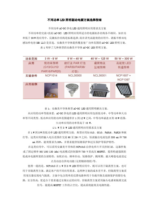
不同功率LED照明驱动电源方案选择指南不同功率AC-DC供电LED通用照明应用要求及方案不同功率的交流-直流(AC-DC) LED照明应用所适合的电源拓扑结构各不相同。
如在功率低于80 W的应用中,反激拓扑结构是标准选择;而在讲究高能效的应用中,谐振半桥双电感加单电容(HB LLC)是首选。
安森美半导体提供覆盖宽广功率范围的AC-DC LED照明方案,表1列举了几种典型的安森美半导体AC-DC LED照明方案。
表1:安森美半导体典型AC-DC LED通用照明解决方案。
从应用的功率等级来看,AC-DC供电的LED通用照明应用包括低功率、中等功率和大功率等不同类型。
低功率应用的功率范围通常在1到12 W之间,中等功率涵盖8到40 W范围,大功率应用的功率常高于40 W。
1)1 W至8 W LED通用照明应用要求及方案在1 W到8 W的低功率LED通用照明方面,典型应用如G13、GU10、PAR16、PAR20和嵌灯等。
这类应用的输入电压范围在交流90至264 V之间,恒流输出电流包括350 mA和700 mA两种,能效要求为80%,并要求提供短路保护和过压保护等保护特性。
在这类应用中,可以采用安森美半导体的NCP1015自供电单片开关控制IC。
这器件集成了固定频率(65/100/130 kHz)电流模式控制器和700 V的高压MOSFET,提供构建强固的低成本电源所需的全部特性,如软启动、频率抖动、短路保护、跳周期、最大峰值电流设定点及动态自供电功能(无需辅助绕组)等。
值得一提的是,NCP1015在1 W到8 W LED照明应用中,既可以用于隔离型方案,也可用于非隔离型方案,满足客户的不同应用需求。
这两种方案的成本差不多。
但隔离型方案采用变压器实现电气隔离,方案中包含简单的反馈电路和用于负载开路及故障保护的钳位电路,安全性高,更适合于需求通过安规认证的应用。
非隔离型方案采用抽头电感来隔离交流信号,能提高MOSFET工作的占空比,提高系统能效及电路性能。
LED通用照明驱动方案

LED通用照明驱动方案11 低功率LED驱动器特征及选择关键点小功率LED电源通常以恒流驱动, 其恒压功效是在输出开路情况下做为保护功效。
小功率LED驱动器特征如图1所表示。
图1: 小功率LED驱动器特征LED驱动器关键功效, 就是在工作条件范围下限制电流, 而不管输入及输出条件怎样改变。
其应用设计面临多个限制条件, 如高能效(低损耗)、高性价比、宽环境条件、高可靠性、灵活、符合电磁干扰(EMI)及谐波含量等方面标准、可改造用于已经有应用及能采取传统控制方法工作等。
要为低功率LED应用选择适合驱动器并不轻易, 需要顾及不一样原因。
比如, 商业和住宅市场对LED灯具在工作温度、使用时长、性能及“能源之星”等行业标准方面要求并不相同。
另外, 灯泡替换应用也存在着独特挑战, 如LED电源及驱动器热度限制、尺寸受限及兼容调光技术等。
就LED通用照明适用标准而言, 关键有美国“能源之星”要求功率因数校正(PFC)标准以及欧盟国际电工委员会(IEC)对总谐波失真限制标准。
其中, “能源之星”V1版灯具标准是自愿性标准, 要求LED照明灯具含有PFC, 适适用于嵌灯、橱柜灯及台灯等特定产品, 但与功率电平无关。
这标准要求住宅应用功率因数(PF)高于0.7, 而商业应用高于0.9。
如前所述, 为低功率LED照明应用选择适合驱动器须考虑众多原因, 这其中, 相关功率因数等行业标准尤为关键。
接下来, 我们将以安森美半导体几款低功率LED通用照明驱动方案为例, 探讨怎样在低功率照明应用中提供高功率因数。
2 DC-DC供电低功率LED照明应用方案LED通用照明有AC-DC供电和DC-DC供电两种方法, 其中AC-DC供电低功率LED通用照明应用及方案在第一讲LED照明驱动方案选型中已经大致介绍过, 所以在此不做赘述, 本讲关键依据功率不一样来介绍DC-DC供电低功率LED通用照明方案。
2.1 1 W-3 W DC-DC LED降压应用经典1 W-3 W DC-DC LED降压照明应用包含MR11/MR16、汽车照明、太阳能供电等。
LED通用照明驱动方案2

LED通用照明驱动方案22.4 1 W-30 W DC-DC LED降压应用典型1 W-30W DC-DC LED降压应用包括MR16射灯、街道照明中的次级端DC-DC LED驱动器。
这类应用中,输入电压范围为7 至120 Vdc,输出电压范围为6至110 Vdc,支持350 mA、700 mA或1 A恒流输出,能效不低于90%。
这类应用可以采用NCL30100降压LED驱动器,这器件外置开关MOSFET,提供灵活的输入电压和输出电流设计,能效高于95%,其应用电路图参见图5。
图5:基于NCL30010的1-30 W DC-DC LED降压应用3 改善低功率LED住宅照明应用能效的方案以住宅照明的台灯和橱柜灯等应用为例,功率一般在3 W到8 W之间。
这样的低功率应用最适合采用隔离型反激拓扑结构。
但传统离线反激电源转换器在开关稳压器前面采用全波整流桥及大电容,这种配置的功率利用率或输入线路波形的PF较低,仅在0.5至0.6的范围。
这就要引入PFC。
如可在反激转换器前采用NCP1607B这样的有源PFC,能提供高于0.98的PF,但增加了元件数量及复杂性,且最适合的功率远高于本应用要求。
无源PFC方案众多,可改善PF,但通常都使用较多额外元件,增加成本及电路板占用空间,并降低可靠性。
图6:改善了功率因数的NCP1014应用电路图实际上,高功率因数通常需要正弦线路电流,且要求线路电流及电流之间的相位差极小。
修改传统设计的第一步就是在开关段前获得极低电容,从而支持更贴近正弦波形的输入电流。
这使整流电压跟随线路电压,产生更合意的正弦输入电流,反激转换器的输入电压就以线路频率的2倍跟随整流正弦电压波形。
如果输入电流保持在相同波形,功率因数就高。
NCP1014自供电单片开关稳压器采用固定频率工作,电流不能上升到高于某个特定点;这个点由输入电压及开关周期或导电时间结束前的初级电感来确定。
由于导电时间的限制,输入电流将跟随输入电压的波形,从而提供更高的功率因数。
大功率、高亮度LED的驱动方案大全

Driving high power and high brightness LEDsApplication Note 5310Figure 1. Series connection(a) Series of two LEDs (b) Series of ‘n’ LEDs.Series connectionFigure 1 shows the series connection. The LED current in the series is the same throughout the series. Its disadvan-tage is that if one LED is opened, no LED will light up. The total VF across the series LED is higher, but the current re-quirement is lower.The LED driver circuit used must be capable of producing output LED voltage greater than the series total VF. Generally, the closer the rated LED output voltage to the series LED total VF, the better is the efficiency.Common anode or common cathode parallel connectionThe common anode or common cathode parallel con-nection is used if each individual LED current is set inde-pendently. The advantage of this connection is that if one LED is opened, the other LEDs are unaffected. The disad-vantage of this connection is that a higher current rating is needed.Common anode and common cathode parallel connectionThe difference between the LED forward voltages will cause current hogging. In cases where this is unavoid-able, use the smallest number of LEDs with matched electrical, thermal and operating lifetime characteristic. The matched LEDs are equivalent to a single larger LED with a higher current rating. However, the matched LEDs may drift apart due to different degradation and thermal characteristics.IntroductionThis paper describes the various methods of driving the high power and high brightness LED. The task of designing an LED based system involves the following selection.I. number of LED used and the connection scheme between LEDsII. linear or switch mode LED driverIII. power supply source i.e. DC voltage or AC mains or batteryIV. optical subsystem, e.g. lens, filter cover etc.The number of LED needed depends on the luminance required and the current the LEDs are driven.The optical subsystem is not covered here as it is beyond the scope of this paper.LED connection schemeIf there is more than one LED, the LED connection scheme must be decided.There is no hard and fast rule in selecting the connection scheme. Sometimes it is a matter of preference. In some cases, the LED drivers chosen will decide the connection scheme. At times, the available power supply and effi-ciency required may influence the connection scheme.Typically, the connection between LED is classified into three main configurations.a) Series b) ParallelThis is subdivided into i) Common anode ii) Common cathodeiii) Common anode and common cathode c) Mixed series – parallel i) Series of two LEDs II) Series of ‘n’ LEDsMixed series - parallel connectionFigure 3 shows some examples of mixed series – parallel connection. This is usually selected as a trade off between the total VF and the total current required, so that it will fit with available led drivers.Figure 3. Mixed series – parallel connection exampleFigure 2. Parallel connection exampleLED driversThe connection scheme will influence the number of drivers channel needed.Most LED driver typically has a single channel. However, there are some multi channel LED drivers available. Each channel can drive only a single series connected LEDs or a single branch of the parallel connected LED in common anode or common cathode configuration. The following condition must be met to be able to drive the series connected LEDs.a) Output LED driver voltage must be greater than the total VF of the series connected LED b) LED driver constant current output must be higher or equal to the desired LED current. If the current is higher, use PWM dimming or modify the circuit, for example the sense resistor.In general, LED drivers are classified into:a) Linear LED driverb) Switch mode LED driverLinear LED driver are less efficient and generally occupy a larger space. Switch mode LED driver is more efficient and generally smaller. However, they have electrical and radiated noise and are complicated to design.When the input power supply is lower than the LEDs total VF, switch mode LED driver must be used. The selectionbetween linear or switch mode is generally decided by simplicity, the available power supply and efficiency.Common Common Common anode &anode Cathodecommon cathodeConverting a voltage regulator to LED driverA typical voltage regulator has the following pins, V IN , GND, V OUT and FB. The FB pin sense a voltage to control the voltage regulator output voltage. For a constant current LED driver, current sense is necessary. By placing a resistor in the LED current path, the LED current is converted to a sense voltage at the FB pin. The resistor is usually placed at the LED cathode side for low side current sensing. Alternatively, the resistor is placed on the LED anode side for high side current sensing. A differential amplifer with high common mode rejection ratio is needed to sense the voltage across the resistor.Figure 4. Converting a voltage regulator to LED driverThe resistor value for low side current sensing isLEDFBI V However, for high side current sensing, the resistor value required isVLED A I V *Note:V FB is the regulated feedback voltage at the FB pin. I LED is the desired LED current.A V is the gain of the differential amplifier.For linear LED driver, the number of LEDs that can be driven in series is N = FRDO IN V V V V --For the switch mode LED driver, the number of LEDs is N =FROR V V V -Note:V IN is the input voltage supply.V DO is the drop out voltage.V R is the sense voltage across the resistor.V OR is the rated designed output voltage of the series connected LED string.V F is the typical forward voltage of a single LED.(a) Low side current sensing(b) High side current sensingLinear LED driver examples 1. Simple resistive current limiting.A resistor is used to limit the LED current from a DC power supply.Figure 6. LM317HV LED driverThe LM317HV regulates a fixed 1.23V between the ADJ and the OUT pin. The LED current is given by the equation, LED = R1.23I The advantage of this circuit over the simple resistive driver is that the LED current is constant despite the LED forward voltage drift.Figure 5. Resistor as a current limiter The resistance is given by R =FFIN I V V -Notes:V F - total VF of the series connected LED string.I F - desired LED current.V IN – input voltage supply.The advantage of simple resistive limiting is the simplicity. However, the LED current is not stable due to LED forward voltage drift.2. LM317 or LM317HVFigure 6 showed the LM317HV voltage regulator used as an LED driver.Figure 8. LT3021 LED driverIf the LED Vf is 3.6V, the number of series connected LED is two.Figure 7. LM2941 LED driverAnother driver similar to the LM317 is the LM2941. The LM2941 voltage regulator has a maximum input voltage of 26V. The LM2941 regulates 1.275V across the ADJ and GND terminal. Figure 7 show the LM2941 as an LED driver providing 354mA.4. LT3021The LT3021 is another linear voltage regulator with maximum input voltage at 10V and a maximum current rating of 500mA. The LT3021 regulates the output to maintain 0.2V across the ADJ and GND terminal. The LED current is R0.2The drop out voltage is 160mV.V REF is regulated to 177mV between ADJ and GND pins.The maximum input voltage rating is 42V with a dropout voltage of 0.7V. The LED current in the circuit isIn the circuit shown in figure 9, R = 5.1ohm. The LED current is 347 mA.Figure 9. Infineon TLE4242G LED driverRV REF 6. AS3691 and AS3692The AS3691 has a voltage rating of 15V with maximum LED current of 400mA.The AS3692 is similar to AS3691. The difference is the AS3692 has a voltage rating up to 50V, but the maximum current is 200mA.Contact Austriamicrosystem for latest information on availability and application notes on AS3691 and AS3692.Figure 10. Maxim 16800 LED driverFor LED color management application with the ADJD-J823 and the HDJD-J822, the PWM output from the ADJD-J823/HDJD-J822 is connected to the EN input of the MAX16800.This LED driver has a voltage rating of 40V. The driver regulates a fixed voltage across the CS+ and CS- The current is set by an external resistor, Notes:I LED is the desired LED currentV SENSE is typically 0.204V across CS+ and CS- pins.R S = LEDSENSEI VFigure 11. HV9911 in boost topologyNotes:1. V REF is typically 1.25V.2. The maximum LED current for this circuit is 350mA.The LED current is related to the equation, 10131213**R I R R R V LED REF =+)(The switch mode LED driver is related to the switching voltage regulator topologies. The switching voltage regulator maintains a constant voltage at various current loads. The switch mode LED driver however, deliver constant current to LED at whatever VF the LEDs required, provided that the over voltage protection or power rating is not exceeded. Some common examples of switch mode LED driver topologies area) BUCK. These are step down regulator which the output voltage is generally lower than the input voltage.b) BOOST. These are step up regulator which the output voltage is higher than the input.c) BUCK-BOOST. These are step down / step up regulator which the output voltage is inverted. d) SEPIC. This is similar to buck boost except the output voltage is not inverted.e) FLYBACK. These are step up or step down regulator with a transformer instead of an inductor.Designers should obtain information on the IC datasheets and application notes from the manufacturer and work closely with the LED driver manufacturer.Before turning on a switch mode LED driver, the LEDs should be connected. An open circuit in the switch mode LED will cause the output voltage to rise to maximum limit and may exceed the LED driver maximum voltage rating.Switch mode LED driver examples1. HV9911 in boost topologyThe input voltage (21-27V) is provided between VIN and GND. This boost topology circuit provides 80V maximum output voltage. I.e. the number of InGaN LEDs that can be driven is 12 to 20 LEDs. If the PWM is not used, it should be connected to VDD to enable the LED driver.Figure 12. HV9911 in buck topology2. HV9911 in buck topologyThis buck topology circuit accepts 130 to 200 V DC input between VIN and GND. It can provide 20 to 100V LED output voltage. The high side current sensing limit the LED current to 350mA. If the PWM is not used, it should be connected to VDD to enable the LED driver.The LED current is related to the equation,Notes:1. V REF is typically 1.25V.2. The maximum LED current for this circuit is 350mA.10131213**R I R R R V LED REF =+)(3. HV9910This buck topology circuit is not isolated from line voltage. The LEDs must be connected to the driver before turning on the AC supply.Table 1 shows the possible VAC input range with this circuit. The components L1 and R4 values are selected based on the operating LED current. Assuming that the LED forward voltage is 3.6V, the maximum number of LED that can be driven is approximately eleven.Table 1. Component selection.VAC Input range VAC Input setting L1L1 Part *R4 ohm LED current mA Output LED driver voltage min max0- V 0VAC . mH, 0. A PCH- - 0. 0- 0 0 00- V 0VAC . mH, 0. A PCH- - 0. 0- 0 0 00- V 0VAC .0mH, A PCV- - 0 -0 0. ** 0- 00 0 0Notes:* The inductor part numbers are from Coilcraft.** Implemented by two 0.27 ohm resistors connected in parallel.The components values for row 1 and 2 are shown in figure 13.The control PWM signal must be isolated from mains. If the PWM is not used, it should be connected to VDD to enable the LED driver. If any measuring instrument needs to be used, they must also be isolated using isolating transformer.Figure 13. HV9910 in buck topologyThis is a buck LED driver. Table 2 shows the various components values needed to obtain the corresponding LED current.Table 2. Resistor selectionR1R3R4R5R6Rs LED current9.1k5101k8.2k27k0.33350mA9.1k510910 2.4k20k0.2700mANote: The component values for the first row are shown in figure 15 to provide 350mA LED current.The Vdim pad provides an input for linear dimming or inverted logic PWM dimming. At 0V, the LED current is maximum. As the voltage increase from 0V to 3.3V, the LED current will reduce linearly from maximum to zero. Resistor R1 and R3 provide over voltage protection at 23.3V in case an open circuit occur at the LED output. AssumingInGaN LEDs with VF = 3.6V, the maximum number of LEDs that can be connected in series is 6 InGaN LEDs.Figure 14. L6902D LED driverThis is a buck topology LED driver with 48V input. A maximum of 12 InGaN LEDs can be connected. Resistors R1, R2 and the internal 5.1V supply reduced the sense voltage to 0.5V.Figure 15. L4973V3.3 LED driverFigure 16. LTC3490 driving a single LED6. LTC3490This circuit is able to drive one InGaN LED from a single battery cell. An internal sense resistor limits the LED outputcurrent to 350mA. If the LED pin is open, the output voltage is internally limited to 4.7V.Figure 17. LTC3783 LED driverThis flyback LED driver can provide 150mA to a series connected LEDs. The over voltage protection is trigger at 130V and deactivate at 120V. The number of series LEDs that can be connected is 120/3.6 = 33 LEDs. PWM signal provide thedimming control.Figure 18. LM3402 LED driver8. LM3402This is a step down buck LED driver. It has a constant on time architecture and the circuit is designed for a single INGAN LED. Refer to the web site below for other LM3402 reference design for other LED output voltage. /webench/ledrefdesigns.doFigure 19. Maxim MAX5035 LED driver9. Maxim 5035.This buck topology circuit accepts Vin from 7.5V to 30V. The LED current is 350mA. The rated LED output voltage is 12V. One to three InGaN LEDs can be driven.V CONTROL is a linear dimming input and the LED current is given by the equation below.I LED = SENSECONTROL REFR5 * R R1V ** (R1 + R5) - V Notes:R SENSE is the parallel equivalent of R2, R3 and R4.V REF is typically 1.22V.V CONTROL is the external linear dimming voltage, 0V for maximum LED current.Table 3 shows the component changes needed to drive 10 LEDs in a series. Table 3. Component changes required for different operating LED current.LED color Total VF range LED current RON L1L1 partRsns Red to 00mA 0k 0uH SLF 0 T- MR 0. Green or Blue0 to0mAk0uHSLF 0 T- MR.Note: The inductor parts are from TDK.10. MAX16801 / MAX16802The MAX 16801 is suitable for rectified 85VAC to 265VAC applications.The MAX16802 is suitable for low input DC input voltage.An example of the MAX16802 driver is shown in Figure 21.This circuit is design for driving a single InGaN LED at 350mA.For other configuration, refer to AN3639, under design procedure.The DC input voltage is from 10.8 to 24V. Resistor, R1 and R2 clamped the output voltage to 29V.Figure 20. MAX16802B LED driverReference1. AND8109/D LED constant current scheme. Theory of operation./pub/Collateral/AND8109-D.PDF2. Datasheets: LM317HV, LM2941, LT3021, TLE4242G, MAX16800, HV9911, HV9910, L6902D, L4973, LTC4930,LTC3783, LM3402, MAX5035, MAX16801/MAX16802.3. AS3691, AS3692 product brief./03products/products_detail/AS3691/download/AS3691_Features.pdf4. HV9911DB1v2 High brightness boost LED driver with 1:3000 dimming ratio and excellent current regulation./feature_hv9911.html5. HV9911DB3 High brightness step-down LED driver with excellent current regulation./feature_hv9911.html6. AN-H55 Boost Converter LED Drivers using Supertex’s HV9911./feature_hv9911.html7. HV9910DB1 Off-line high brightness LED driver board./feature_hv9910.html8. HV9910DB2v2 Universal voltage off-line high brightness LED driver demo board./feature_hv9910.html9. AN-H48 Buck-based LED Drivers using the HV9910/HV9910B./feature_hv9910.html10. AN2129 Dimming of super high brightness LEDs with L6902./stonline/products/literature/an/11247.pdf11. AN1891 Driving LEDs using L497X, L597X, L692X DC-DC converters families. /stonline/products/literature/an/10232.pdf12. High Voltage Boost/LED Controller Provides 3000:1 PWM Dimming Ratio. Linear Technology Magazine March2006. /pc/downloadDocument.do?navId=H0,C1,C1003,C1042,C1031,C1115,P15692,D14232 13. Maxim AN3668 High-Efficiency Current Drive for High-Brightness LEDs./en/an/AN3668.pdf14. Maxim AN3639 Design of a Nonisolated, Flyback LED Driver Circuit./en/an/AN3639.pdf15. How to use switching regulators in driving high brightness LEDs By Chris Richardson./howto/183702675 or/news/183701658Avago Technologies reserve the right to make corrections, modifications, enhancements, improvements, and other changes to this documents at any time. Customers should obtain the latest document and should verify that the infor-mation is current and complete.Avago Technologies assumes no liability for applications assistance or customer product design using the informa-tion provided in this document. Customers are responsible for their products and applications using Avago Technolo-gies products. Customers should provide adequate design and operating margin to minimize the risks associated with customer products and applications.Avago Technologies does not warrant or represent that any license, either express or implied, is granted under any Avago Technologies patent right, copyright, or other intellectual property right relating to any design and process in this document. Information regarding third-party products or services does not constitute a license from Avago Tech-nologies to use such products or services or a warranty or endorsement thereof. The use of such information may require a license from a third party under the patents.For product information and a complete list of distributors, please go to our web site: Avago, Avago Technologies, and the A logo are trademarks of Avago Technologies, Limited in the United States and other countries.Data subject to change. Copyright © 00 Avago Technologies Limited. All rights reserved. Obsoletes AV0 -0 0ENAV0 -0 EN - June , 00。
led驱动方案

led驱动方案在现代社会中,LED灯具的市场需求越来越大,这也催生了许多厂商的加入。
然而,研发一个高质量且经济实惠的LED驱动方案可不是一件容易的事情。
本文将介绍几种LED驱动方案以及它们各自的优缺点,希望能够给大家提供一些参考。
一、常见的1.1 恒压驱动恒压驱动是一种非常简单的模式,它解决了LED灯泡的电压问题,并使它们在过程中的增光保持恒定。
当然,这种方案也有一些限制,LED所需的功率或者电流必须非常低。
1.2 恒流驱动恒流驱动是在LED灯普及后出现的一种驱动方式。
它可以提供足够的电流,使LED灯发光,同时,也可以在大功率应用中为LED灯提供保护。
这种方案的优点是变化仅限于输入、输出和驱动电压之间的匹配度。
1.3 功率因数修正功率因数是测量电力线路效率的一项标准。
不理想的功率因数会使电线损失能量并浪费电能。
在这种情况下,功率因数修正技术成为了解决方法,同时也有效地减少了电能的浪费。
一、LED驱动方案的优缺点2.1 恒压驱动优点:能够提供代表灯泡最高限制电压的电压;温暖的光具有一定的质量以及盈亮效果。
缺点:不足以控制LED的输出亮度;当使用高电压时,LED可能会短路或者过热。
2.2 恒流驱动优点:使LED灯具消耗的电流保持不变;使光变得更加柔和,不会使眼睛受到刺激;有更长的使用寿命。
缺点:需要预留适当的保护裕度;更高的成本。
2.3 功率因数修正优点:提高了电能的使用效率;减少了电路损耗;使用更智能、更节能的电源。
缺点:价格较高。
三、LED驱动方案如何选择LED灯驱动方案可以根据具体情况选择。
如果预算允许,而且希望LED灯具具有更高的性能,并且使用寿命更长,那么恒流驱动或功率因数修正方案就是不错的选择。
然而,如果需要使用的LED灯泡只需要输出低功率,则恒压驱动方案可能更加合适。
最终选择何种方案还需看情况灵活决定。
总之,为了保证LED灯具的稳定性和安全性,选择合适的驱动方案是很有必要的。
从经济、安全和可靠性角度考虑,选择高质量的驱动方案,才能更好地实现期望的光效与服务寿命。
- 1、下载文档前请自行甄别文档内容的完整性,平台不提供额外的编辑、内容补充、找答案等附加服务。
- 2、"仅部分预览"的文档,不可在线预览部分如存在完整性等问题,可反馈申请退款(可完整预览的文档不适用该条件!)。
- 3、如文档侵犯您的权益,请联系客服反馈,我们会尽快为您处理(人工客服工作时间:9:00-18:30)。
不同功率等级的LED照明驱动方案介绍
中心议题:
●线性恒流稳压器驱动LED
●电感型转换器驱动LED
●可使用TRIAC调光的LED驱动方案
●LED日光灯驱动方案
●LED路灯照明解决方案
凭借着节能、高效、长使用寿命等优势,LED照明成为当下异常火热的一个领域。
欧美、日本各国纷纷出台政策支持LED照明的发展。
LED照明的发展催生了LED驱动器巨大的市场需求。
本文将按照电流的等级来介绍几种用于不同领域的LED照明驱动方案。
市场上典型的LED驱动器包括两类,即线性驱动器和开关驱动器;大概的适用范围见图1。
如电流大于500mA的大电流应用采用开关稳压器,因为线性驱动器限于自身结构原因,无法提供这样大的电流;而在电流低于200mA 的低电流应用中,通常采用线性稳压器或分离稳压器;而在200至500mA的中等电流应用中,既可以采用线性稳压器,也可以采用开关稳压器。
开关稳压器的能效高,且提供极佳的亮度控制。
线性稳压器结构比较简单,易于设计,提供稳流及过流保护,且没有电磁兼容性(EMC)问题。
图1 LED驱动器分类
线性恒流稳压器
在低电流LED应用中,电阻型驱动器尽管成本较低且结构简单,但这种驱动器在低电压条件下,正向电流较低,会导致LED亮度不足,且在负载突降。