uln2803a中文资料2
一文看懂uln2803和uln2003区别
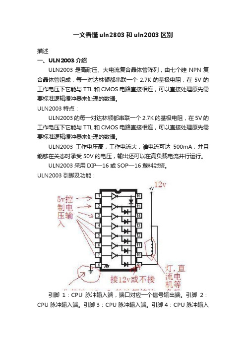
一文看懂uln2803和uln2003区别描述一、ULN2003介绍ULN2003是高耐压、大电流复合晶体管阵列,由七个硅NPN复合晶体管组成,每一对达林顿都串联一个2.7K的基极电阻,在5V的工作电压下它能与TTL和CMOS电路直接相连,可以直接处理原先需要标准逻辑缓冲器来处理的数据。
ULN2003特点:ULN2003的每一对达林顿都串联一个2.7K的基极电阻,在5V的工作电压下它能与TTL和CMOS电路直接相连,可以直接处理原先需要标准逻辑缓冲器来处理的数据。
ULN2003工作电压高,工作电流大,灌电流可达500mA,并且能够在关态时承受50V的电压,输出还可以在高负载电流并行运行。
ULN2003采用DIP—16或SOP—16塑料封装。
ULN2003引脚及功能:引脚1:CPU脉冲输入端,端口对应一个信号输出端。
引脚2:CPU脉冲输入端。
引脚3:CPU脉冲输入端。
引脚4:CPU脉冲输入端。
引脚5:CPU脉冲输入端。
引脚6:CPU脉冲输入端。
引脚7:CPU脉冲输入端。
引脚8:接地。
引脚9:该脚是内部7个续流二极管负极的公共端,各二极管的正极分别接各达林顿管的集电极。
用于感性负载时,该脚接负载电源正极,实现续流作用。
如果该脚接地,实际上就是达林顿管的集电极对地接通。
引脚10:脉冲信号输出端,对应7脚信号输入端。
引脚11:脉冲信号输出端,对应6脚信号输入端。
引脚12:脉冲信号输出端,对应5脚信号输入端。
引脚13:脉冲信号输出端,对应4脚信号输入端。
引脚14:脉冲信号输出端,对应3脚信号输入端。
引脚15:脉冲信号输出端,对应2脚信号输入端。
引脚16:脉冲信号输出端,对应1脚信号输入端。
ULN2003作用:ULN2003是大电流驱动阵列,多用于单片机、智能仪表、PLC、数字量输出卡等控制电路中。
可直接驱动继电器等负载。
输入5VTTL电平,输出可达500mA/50V。
ULN2003是高耐压、大电流达林顿系列,由七个硅NPN达林顿管组成。
ULS2803中文资料
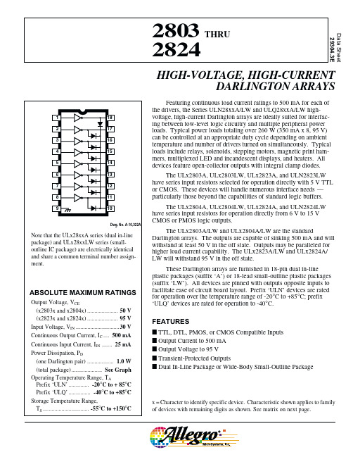
2803 THRU 2824HIGH-VOLTAGE,HIGH-CURRENT DARLINGTON ARRAYSTest Applicable Limits Characteristic Symbol Fig.DevicesTest Conditions Min.Typ.Max.Units Output Leakage CurrentI CEX1A All V CE = 50 V, T A = 25°C —< 150µA V CE = 50 V, T A = 70°C—< 1100µA 1BULx2804xV CE = 50 V, T A = 70°C, V IN = 1.0 V —< 5500µA Collector-Emitter V CE(SAT)2AllI C = 100 mA, I B = 250 µA —0.9 1.1V Saturation Voltagel C = 200 mA, I B = 350 µA — 1.1 1.3V I C = 350 mA, I B = 500 µA— 1.3 1.6V Input CurrentI IN(ON)3ULx2803x V IN = 3.85 V —0.93 1.35mA ULx2804xV IN = 5.0 V —0.350.5mA V IN = 12 V— 1.0 1.45mA I IN(OFF)4All l C = 500 µA, T A = 70°C 5065—µA Input VoltageV IN(ON)5ULx2803xV CE = 2.0 V, l C = 200 mA —— 2.4V V CE = 2.0 V, I C = 250 mA —— 2.7V V CE = 2.0 V, l C = 300 mA—— 3.0V ULx2804xV CE = 2.0 V, l C = 125 mA —— 5.0V V CE = 2.0 V, l C = 200 mA —— 6.0V V CE = 2.0 V, I C = 275 mA ——7.0V V CE = 2.0 V, l C = 350 mA——8.0V Input Capacitance C IN —All —1525pF Turn-On Delay t PLH 8All 0.5 E IN to 0.5 E OUT —0.25 1.0µs Turn-Off Delay t PHL 8All 0.5 E IN to 0.5 E OUT —0.25 1.0µs Clamp Diode I R 6All V R = 50 V, T A = 25°C ——50µA Leakage Current V R = 50 V, T A = 70°C ——100µA Clamp Diode V F7AllI F = 350 mA—1.72.0VForward VoltageComplete part number includes prefix to operating temperature range: ULN = -20°C to +85°C, ULQ = -40°C to +85°C and a suffix to identify package style: A = DIP, LW = SOIC.Types ULx2803A, ULx2803LW, ULx2804A, and ULx2804LWELECTRICAL CHARACTERISTICS at +25°C (unless otherwise noted).2803 THRU 2824HIGH-VOLTAGE,HIGH-CURRENTDARLINGTON ARRAYS115 Northeast Cutoff, Box 15036Worcester, Massachusetts 01615-0036 (508) 853-5000Test Applicable Limits Characteristic Symbol Fig.DevicesTest Conditions Min.Typ.Max.Units Output Leakage CurrentI CEX1A All V CE = 95 V, T A = 25°C —< 150µA V CE = 95 V, T A = 70°C—< 1100µA 1BULx2824xV CE = 95 V, T A = 70°C, V IN = 1.0 V —< 5500µA Collector-Emitter V CE(SAT)2AllI C = 100 mA, I B = 250 µA —0.9 1.1V Saturation Voltagel C = 200 mA, I B = 350 µA — 1.1 1.3V I C = 350 mA, I B = 500 µA— 1.3 1.6V Input CurrentI IN(ON)3ULx2823x V IN = 3.85 V —0.93 1.35mA ULx2824xV IN = 5.0 V —0.350.5mA V IN = 12 V— 1.0 1.45mA I IN(OFF)4All l C = 500 µA, T A = 70°C 5065—µA Input VoltageV IN(ON)5ULx2823xV CE = 2.0 V, l C = 200 mA —— 2.4V V CE = 2.0 V, I C = 250 mA —— 2.7V V CE = 2.0 V, l C = 300 mA—— 3.0V ULx2824xV CE = 2.0 V, l C = 125 mA —— 5.0V V CE = 2.0 V, l C = 200 mA —— 6.0V V CE = 2.0 V, I C = 275 mA ——7.0V V CE = 2.0 V, l C = 350 mA——8.0V Input Capacitance C IN —All —1525pF Turn-On Delay t PLH 8All 0.5 E IN to 0.5 E OUT —0.25 1.0µs Turn-Off Delay t PHL 8All 0.5 E IN to 0.5 E OUT —0.25 1.0µs Clamp Diode I R 6All V R = 95 V, T A = 25°C ——50µA Leakage Current V R = 95 V, T A = 70°C ——100µA Clamp Diode V F7AllI F = 350 mA—1.72.0VForward VoltageComplete part number includes prefix to operating temperature range: ULN = -20°C to +85°C, ULQ = -40°C to +85°Cand a suffix to identify package style: A = DIP, LW = SOIC. Note that the ULQ2823LW and ULQ2824LW are not presently available.Types ULx2823A, ULN2823LW, ULx2824A, and ULN2824LWELECTRICAL CHARACTERISTICS at +25°C (unless otherwise noted).2803 THRU 2824HIGH-VOLTAGE,HIGH-CURRENTDARLINGTON ARRAYS115 Northeast Cutoff, Box 15036Worcester, Massachusetts 01615-0036 (508) 853-500020Dwg. GP-070-44010080DUTY CYCLE IN PER CENT0600400O U T P U T C U R R E N T I N m A /C H A N N E L2006020Dwg. GP-070-34010080DUTY CYCLE IN PER CENT0600400O U T P U T C U R R E N T I N m A /C H A N N E L20060ALLOWABLE COLLECTOR CURRENT AS A FUNCTION OF DUTY CYCLEULx28xxLW20Dwg. GP-070-24010080DUTY CYCLE IN PER CENT 0600400O U T P U T C U R R E N T I N m A /C H A N N E L2006020Dwg. GP-070-14010080DUTY CYCLE IN PER CENT 0600400O U T P U T C U R R E N T I N m A /C H A N N E L20060ALLOWABLE COLLECTOR CURRENT AS A FUNCTION OF DUTY CYCLEULx28xxAx = Characters to identify specific device. Specification shown applies to family of devices with remaining digits as shown.2803 THRU 2824HIGH-VOLTAGE,HIGH-CURRENT DARLINGTON ARRAYSINPUT CURRENT AS AFUNCTION OF INPUT VOLTAGEULx28x3xDwg. GP-069INPUT VOLTAGE2.52.0I N P U T C U R R E N T I N m A — II N1.00.51.50.5Dwg. GP-0671.01.5COLLECTOR-EMITTER SATURATION VOLTAGE0600400C O L L E C T O R C U R R E N T I N m A200COLLECTOR CURRENT AS A FUNCTION OF INPUT CURRENT200Dwg. GP-068400INPUT CURRENT IN µA0600400C O L L E C T O R C U R R E N T I N m A200ULx28x4x6Dwg. GP-069-11012INPUT VOLTAGE52.0I N P U T C U R R E N T I N m A — I I N1.00.51.587911SATURATION VOLTAGE AS A FUNCTION OFCOLLECTOR CURRENTx = Characters to identify specific device. Characteristic shown applies to family of devices with remaining digits as shown.2803 THRU 2824HIGH-VOLTAGE,HIGH-CURRENTDARLINGTON ARRAYS115 Northeast Cutoff, Box 15036Worcester, Massachusetts 01615-0036 (508) 853-5000PACKAGE DESIGNATOR “A” DIMENSIONSDimensions in Inches (controlling dimensions)Dimensions in Millimeters (for reference only)NOTES:1.Exact body and lead configuration at vendor’s option within limits shown.2.Lead spacing tolerance is non-cumulative.3.Lead thickness is measured at seating plane or below.Dwg. MA-001-18A in19Dwg. MA-001-18A mm192803THRU2824HIGH-VOLTAGE,HIGH-CURRENT DARLINGTON ARRAYS PACKAGE DESIGNATOR “LW” DIMENSIONSDimensions in Inches(for reference only)Dimensions in Millimeters(controlling dimensions)Dwg. MA-008-18A mm1.27BSCDwg. MA-008-18A inBSCNOTES:1.Exact body and lead configuration at vendor’s option within limits shown.2.Lead spacing tolerance is non-cumulative.2803 THRU 2824HIGH-VOLTAGE,HIGH-CURRENTDARLINGTON ARRAYS115 Northeast Cutoff, Box 15036Worcester, Massachusetts 01615-0036 (508) 853-5000The products described here are manufactured under one or more U.S. patents or U.S. patents pending.Allegro MicroSystems, Inc. reserves the right to make, from time to time, such departures from the detail specifications as may be required to permit improvements in the performance, reliability, ormanufacturability of its products. Before placing an order, the user is cautioned to verify that the information being relied upon is current.Allegro products are not authorized for use as critical components in life-support devices or systems without express written approval.The information included herein is believed to be accurate and reliable. However, Allegro MicroSystems, Inc. assumes no responsi-bility for its use; nor for any infringement of patents or other rights of third parties which may result from its use.。
ULN2804A中文资料

13
Figure 12. Representative Schematic Diagrams
1/8 ULN2803
2.7 k 7.2 k 3.0 k Pin 10 10.5 k 7.2 k 3.0 k
1/8 ULN2804
Pin 10
4
MOTOROLA ANALOG IC DEVICE DATA
元器件交易网
Figure 2.
Open h FE
+ IC
I
in
µA Open DUT ICEX Vin DUT IC V VCE
Figure 3.
Open VCE
Figure 4.
Open
µA Iin Vin µA µA Vin DUT
DUT
Open
Figure 5.
Open
Figure 6.
VR
µA IR DUT IC Vin V VCE V Open
2
MOTOROLA ANALOG IC DEVICE DATA
元器件交易网
ULN2803 ULN2804
TEST FIGURES
(See Figure Numbers in Electrical Characteristics Table)
Figure 1.
Open VCE
ULN2803 ULN2804
ELECTRICAL CHARACTERISTICS (TA = 25°C, unless otherwise noted)
Characteristic Output Leakage Current (Figure 1) (VO = 50 V, TA = +70°C) (VO = 50 V, TA = +25°C) (VO = 50 V, TA = +70°C, VI = 6.0 V) (VO = 50 V, TA = +70°C, VI = 1.0 V) Collector–Emitter Saturation Voltage (Figure 2) (IC = 350 mA, IB = 500 µA) (IC = 200 mA, IB = 350 µA) (IC = 100 mA, IB = 250 µA) Input Current – On Condition (Figure 4) (VI = 17 V) (VI = 3.85 V) (VI = 5.0 V) (VI = 12 V) Input Voltage – On Condition (Figure 5) (VCE = 2.0 V, IC = 300 mA) (VCE = 2.0 V, IC = 200 mA) (VCE = 2.0 V, IC = 250 mA) (VCE = 2.0 V, IC = 300 mA) (VCE = 2.0 V, IC = 125 mA) (VCE = 2.0 V, IC = 200 mA) (VCE = 2.0 V, IC = 275 mA) (VCE = 2.0 V, IC = 350 mA) Input Current – Off Condition (Figure 3) (IC = 500 µA, TA = +70°C) DC Current Gain (Figure 2) (VCE = 2.0 V, IC = 350 mA) Input Capacitance Turn–On Delay Time (50% EI to 50% EO) Turn–Off Delay Time (50% EI to 50% EO) Clamp Diode Leakage Current (Figure 6) (VR = 50 V) Clamp Diode Forward Voltage (Figure 7) (IF = 350 mA) TA = +25°C TA = +70°C All Types All Types ULN2802 ULN2804 VCE(sat) All Types All Types All Types II(on) ULN2802 ULN2803 ULN2804 ULN2804 VI(on) ULN2802 ULN2803 ULN2803 ULN2803 ULN2804 ULN2804 ULN2804 ULN2804 All Types ULN2801 II(off) hFE CI ton toff IR VF – – – – – – – – 50 1000 – – – – – – – – – – – – – 100 – 15 0.25 0.25 – 1.5 13 2.4 2.7 3.0 5.0 6.0 7.0 8.0 – – 25 1.0 1.0 50 100 2.0 µA – pF µs µs µA V – – – – 0.82 0.93 0.35 1.0 1.25 1.35 0.5 1.45 V – – – 1.1 0.95 0.85 1.6 1.3 1.1 mA Symbol ICEX – – – – – – – – 100 50 500 500 V Min Typ Max Unit µA
uln2803资料介绍

6
V
7
V
8
V
2.4
V
–2
25 pF –
1
µs –
1
µs –
50 µA 6 100 µA 6
2
V7
3/8
ULN2801A - ULN2802A - ULN2803A - ULN2804A - ULN2805A
TEST CIRCUITS Figure 1a.
Figure 1b.
Figure 2.
Figure 3.
MAX. 0.065
0.915
0.280 0.155 0.063
7/8
ULN2801A - ULN2802A - ULN2803A - ULN2804A - ULN2805A
Information furnished is believed to be accurate and reliable. However, SGS-THOMSON Microelectronics assumes no responsibility for the consequences of use of such information nor for any infringement of patents or other rig hts of third parties which may result from its use. No license is granted by implication or otherwise under any patent or patent rights of SGS-THOMSON Microelectronics. Specification mentioned in this publication are subject to change without notice. This publication supersedes and replaces all information previously supplied. SGS-THOMSON Microelectronics products are not authorized for use as critical components in life support devices or systems without express written approval of SGS-THOMSON Microelectronics.
ULN2803ADWG4中文资料
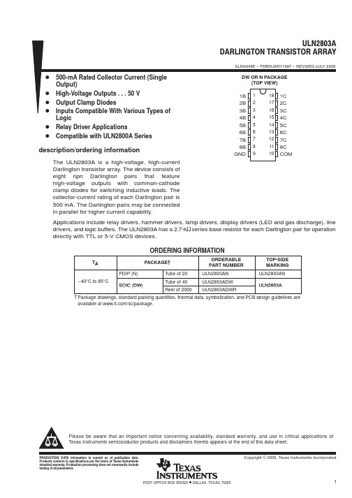
PACKAGING INFORMATIONOrderable Device Status (1)Package Type Package Drawing Pins Package Qty Eco Plan (2)Lead/Ball Finish MSL Peak Temp (3)ULN2803ADW ACTIVE SOIC DW 1840Green (RoHS &no Sb/Br)CU NIPDAU Level-2-260C-1YEAR ULN2803ADWG4ACTIVE SOIC DW 1840Green (RoHS &no Sb/Br)CU NIPDAU Level-2-260C-1YEAR ULN2803ADWR ACTIVE SOIC DW 182000Green (RoHS &no Sb/Br)CU NIPDAU Level-2-260C-1YEAR ULN2803ADWRG4ACTIVE SOIC DW 182000Green (RoHS &no Sb/Br)CU NIPDAU Level-2-260C-1YEAR ULN2803AN ACTIVE PDIP N 1820Pb-Free (RoHS)CU NIPDAU N /A for Pkg Type ULN2803ANE4ACTIVEPDIPN1820Pb-Free (RoHS)CU NIPDAUN /A for Pkg Type(1)The marketing status values are defined as follows:ACTIVE:Product device recommended for new designs.LIFEBUY:TI has announced that the device will be discontinued,and a lifetime-buy period is in effect.NRND:Not recommended for new designs.Device is in production to support existing customers,but TI does not recommend using this part in a new design.PREVIEW:Device has been announced but is not in production.Samples may or may not be available.OBSOLETE:TI has discontinued the production of the device.(2)Eco Plan -The planned eco-friendly classification:Pb-Free (RoHS),Pb-Free (RoHS Exempt),or Green (RoHS &no Sb/Br)-please check /productcontent for the latest availability information and additional product content details.TBD:The Pb-Free/Green conversion plan has not been defined.Pb-Free (RoHS):TI's terms "Lead-Free"or "Pb-Free"mean semiconductor products that are compatible with the current RoHS requirements for all 6substances,including the requirement that lead not exceed 0.1%by weight in homogeneous materials.Where designed to be soldered at high temperatures,TI Pb-Free products are suitable for use in specified lead-free processes.Pb-Free (RoHS Exempt):This component has a RoHS exemption for either 1)lead-based flip-chip solder bumps used between the die and package,or 2)lead-based die adhesive used between the die and leadframe.The component is otherwise considered Pb-Free (RoHS compatible)as defined above.Green (RoHS &no Sb/Br):TI defines "Green"to mean Pb-Free (RoHS compatible),and free of Bromine (Br)and Antimony (Sb)based flame retardants (Br or Sb do not exceed 0.1%by weight in homogeneous material)(3)MSL,PeakTemp.--The Moisture Sensitivity Level rating according to the JEDEC industry standard classifications,and peak solder temperature.Important Information and Disclaimer:The information provided on this page represents TI's knowledge and belief as of the date that it is provided.TI bases its knowledge and belief on information provided by third parties,and makes no representation or warranty as to the accuracy of such information.Efforts are underway to better integrate information from third parties.TI has taken and continues to take reasonable steps to provide representative and accurate information but may not have conducted destructive testing or chemical analysis on incoming materials and chemicals.TI and TI suppliers consider certain information to be proprietary,and thus CAS numbers and other limited information may not be available for release.In no event shall TI's liability arising out of such information exceed the total purchase price of the TI part(s)at issue in this document sold by TI to Customer on an annual basis.PACKAGE OPTION ADDENDUM5-Feb-2007Addendum-Page 1元器件交易网IMPORTANT NOTICETexas Instruments Incorporated and its subsidiaries (TI) reserve the right to make corrections, modifications,enhancements, improvements, and other changes to its products and services at any time and todiscontinue any product or service without notice. Customers should obtain the latest relevant informationbefore placing orders and should verify that such information is current and complete. All products are soldsubject to TI’s terms and conditions of sale supplied at the time of order acknowledgment.TI warrants performance of its hardware products to the specifications applicable at the time of sale inaccordance with TI’s standard warranty. Testing and other quality control techniques are used to the extentTI deems necessary to support this warranty. Except where mandated by government requirements, testingof all parameters of each product is not necessarily performed.TI assumes no liability for applications assistance or customer product design. Customers are responsiblefor their products and applications using TI components. To minimize the risks associated with customerproducts and applications, customers should provide adequate design and operating safeguards.TI does not warrant or represent that any license, either express or implied, is granted under any TI patentright, copyright, mask work right, or other TI intellectual property right relating to any combination, machine,or process in which TI products or services are used. Information published by TI regarding third-partyproducts or services does not constitute a license from TI to use such products or services or a warranty orendorsement thereof. Use of such information may require a license from a third party under the patents orother intellectual property of the third party, or a license from TI under the patents or other intellectualproperty of TI.Reproduction of information in TI data books or data sheets is permissible only if reproduction is withoutalteration and is accompanied by all associated warranties, conditions, limitations, and notices.Reproduction of this information with alteration is an unfair and deceptive business practice. TI is notresponsible or liable for such altered documentation.Resale of TI products or services with statements different from or beyond the parameters stated by TI forthat product or service voids all express and any implied warranties for the associated TI product or serviceand is an unfair and deceptive business practice. TI is not responsible or liable for any such statements.Following are URLs where you can obtain information on other Texas Instruments products and applicationsolutions:Products ApplicationsAmplifiers Audio /audioData Converters Automotive /automotive/broadband DSP BroadbandControl /digitalcontrolDigitalInterface Logic Military /military Power Mgmt Optical Networking /opticalnetworkSecurity /securityMicrocontrollers Low Power Wireless /lpw Telephony /telephonyVideo & Imaging /videoWireless/wirelessMailing Address: Texas InstrumentsPost Office Box 655303 Dallas, Texas 75265Copyright © 2007, Texas Instruments Incorporated。
ULN2803,ULN2804说明书_EN

2803 THRU 2824HIGH-VOLTAGE,HIGH-CURRENTDARLINGTON ARRAYS115 Northeast Cutoff, Box 15036Worcester, Massachusetts 01615-0036 (508) 853-50002Copyright © 1977, 2001 Allegro MicroSystems, Inc.*Also available for operation between -40°C and +85°C. To order, change prefix from ‘ULN’ to ‘ULQ’.DEVICE PART NUMBER DESIGNATION5075100125150AMBIENT TEMPERATURE IN °C25Dwg. GP-018BA L L O W AB L E P AC K A G E P O W E RD I S S I P A T I O N I N W A T T Sx = Character to identify specific device. Specification shown applies to family of devices with remaining digits as shown. See matrix above.The ULx2804, ULx2823, & ULx2824 are discontinued.Shown for reference only.2803 THRU 2824HIGH-VOLTAGE,HIGH-CURRENT DARLINGTON ARRAYS3Complete part number includes prefix to operating temperature range: ULN = -20°C to +85°C, ULQ = -40°C to +85°C and a suffix to identify package style: A = DIP, LW = SOIC.Types ULx2803A, ULx2803LW, ULx2804A, and ULx2804LWELECTRICAL CHARACTERISTICS at +25°C (unless otherwise noted).The ULx2804 is discontinued.Shown for reference only.2803 THRU 2824HIGH-VOLTAGE,HIGH-CURRENTDARLINGTON ARRAYS115 Northeast Cutoff, Box 15036Worcester, Massachusetts 01615-0036 (508) 853-50004Complete part number includes prefix to operating temperature range: ULN = -20°C to +85°C, ULQ = -40°C to +85°Cand a suffix to identify package style: A = DIP, LW = SOIC. Note that the ULQ2823LW and ULQ2824LW are not presently available.Types ULx2823A, ULN2823LW, ULx2824A, and ULN2824LWELECTRICAL CHARACTERISTICS at +25°C (unless otherwise noted).The ULx2823 & ULx2824 are discontinued.Shown for reference only.2803 THRU 2824HIGH-VOLTAGE,HIGH-CURRENTDARLINGTON ARRAYS115 Northeast Cutoff, Box 15036Worcester, Massachusetts 01615-0036 (508) 853-5000620Dwg. GP-070-44010080DUTY CYCLE IN PER CENT0600400O U T P U T C U R R E N T I N m A /C H A N N E L2006020Dwg. GP-070-34010080DUTY CYCLE IN PER CENT0600400O U T P U T C U R R E N T I N m A /C H A N N E L20060ALLOWABLE COLLECTOR CURRENT AS A FUNCTION OF DUTY CYCLEULx28xxLW20Dwg. GP-070-24010080DUTY CYCLE IN PER CENT 0600400O U T P U T C U R R E N T I N m A /C H A N N E L2006020Dwg. GP-070-14010080DUTY CYCLE IN PER CENT 0600400O U T P U T C U R R E N T I N m A /C H A N N E L20060ALLOWABLE COLLECTOR CURRENT AS A FUNCTION OF DUTY CYCLEULx28xxAx = Characters to identify specific device. Specification shown applies to family of devices with remaining digits as shown.2803 THRU 2824HIGH-VOLTAGE,HIGH-CURRENT DARLINGTON ARRAYS7INPUT CURRENT AS AFUNCTION OF INPUT VOLTAGEULx28x3xDwg. GP-069INPUT VOLTAGE2.52.0I N P U T C U R R E N T I N m A — II N1.00.51.50.5Dwg. GP-0671.01.5COLLECTOR-EMITTER SATURATION VOLTAGE0600400C O L L E C T O R C U R R E N T I N m A200COLLECTOR CURRENT AS A FUNCTION OF INPUT CURRENT200Dwg. GP-068400INPUT CURRENT IN µA0600400C O L L E C T O R C U R R E N T I N m A200ULx28x4x6Dwg. GP-069-11012INPUT VOLTAGE52.0I N P U T C U R R E N T I N m A — II N1.00.51.587911SATURATION VOLTAGE AS A FUNCTION OFCOLLECTOR CURRENTx = Characters to identify specific device. Characteristic shown applies to family of devices with remaining digits as shown.2803 THRU 2824HIGH-VOLTAGE,HIGH-CURRENTDARLINGTON ARRAYS115 Northeast Cutoff, Box 15036Worcester, Massachusetts 01615-0036 (508) 853-50008PACKAGE DESIGNATOR “A” DIMENSIONSDimensions in Inches (controlling dimensions)Dimensions in Millimeters (for reference only)NOTES:1.Exact body and lead configuration at vendor’s option within limits shown.2.Lead spacing tolerance is non-cumulative.3.Lead thickness is measured at seating plane or below.Dwg. MA-001-18A in19Dwg. MA-001-18A mm192803 THRU 2824HIGH-VOLTAGE,HIGH-CURRENT DARLINGTON ARRAYS9PACKAGE DESIGNATOR “LW” DIMENSIONSDimensions in Inches (for reference only)Dimensions in Millimeters (controlling dimensions)Dwg. MA-008-18A mm1.27BSCwg. MA-008-18A inBSCNOTES:1.Exact body and lead configuration at vendor’s option within limits shown.2.Lead spacing tolerance is non-cumulative.2803 THRU 2824HIGH-VOLTAGE,HIGH-CURRENTDARLINGTON ARRAYS115 Northeast Cutoff, Box 15036Worcester, Massachusetts 01615-0036 (508) 853-500010The products described here are manufactured under one or more U.S. patents or U.S. patents pending.Allegro MicroSystems, Inc. reserves the right to make, from time to time, such departures from the detail specifications as may be required to permit improvements in the performance, reliability, ormanufacturability of its products. Before placing an order, the user is cautioned to verify that the information being relied upon is current.Allegro products are not authorized for use as critical components in life-support devices or systems without express written approval.The information included herein is believed to be accurate and reliable. However, Allegro MicroSystems, Inc. assumes no responsi-bility for its use; nor for any infringement of patents or other rights of third parties which may result from its use.This datasheet has been download from: Datasheets for electronics components.。
uln2803a中文资料2
要:ULN2000、ULN2800是高压大电流达林顿晶体管阵列系列产品,具有电流增益高、工作电压高、温度范围宽、带负载能力强等特点,适应于各类要求高速大功率驱动的系统。
ULN2003A电路是美国Texas Instruments公司和Sprague公司开发的高压大电流达林顿晶体管阵列电路,文中介绍了它的电路构成、特征参数及典型应用。
关键词:达林顿晶体管阵列驱动电路ULN2003 ULN2000系列ULN2800系列1 概述功率电子电路大多要求具有大电流输出能力,以便于驱动各种类型的负载。
功率驱动电路是功率电子设备输出电路的一个重要组成部分。
在大型仪器仪表系统中,经常要用到伺服电机、步进电机、各种电磁阀、泵等驱动电压高且功率较大的器件。
ULN2000、ULN2800高压大电流达林顿晶体管阵列系列产品就属于这类可控大功率器件,由于这类器件功能强、应用范围语广。
因此,许多公司都生产高压大电流达林顿晶体管阵列产品,从而形成了各种系列产品,ULN2000、ULN2800系列就是美国Texas Instruments公司、美国Sprague公司开发的高压大电流达林顿晶体管阵列产品。
它们的系列型号分类如表1所列,生产2000、2800高压大电流达林顿晶体管阵列系列产品的公司与型号对照表如表2所列。
在上述系列产品中,ULN2000系列能够同时驱动7组高压大电流负载,ULN2800系列则能够同时驱动8组高压大电流负载。
美国Texas Instruments公司、美国Sprague公司生产的ULN2003A由7组达林顿晶体管阵列和相应的电阻网络以及钳位二极管网络构成,具有同时驱动7组负载的能力,为单片双极型大功率高速集成电路。
以下介绍该电路的构成、性能特征、电参数以及典型应用。
2000、2800高压大电流达林顿晶体管阵列系列中的其它产品的性能特性与应用可参考ULN2003A。
表1 ULN2000、ULN2800系列型号分类表输出电压50V50V95V50V50V95V输出电流500mA600mA500mA500mA600mA500mA型号型号普通PMOS、CMOS输入ULN2001A ULN2011A ULN2021ULN2801A ULN2811A ULN2821A 14~25C PMOS输入ULN2002A ULN2012A ULN2022ULN2802A ULN2812A ULN2822A 5V TTL、CMOS输入ULN2003A ULN2013A ULN2023A ULN2803A ULN2813A ULN2823A 6~15V PMOS、CMOS输入ULN2004A ULN2014A ULN2024A ULN2804A ULN2814A ULN2824A 高输出TTL接口ULN2005A ULN2015A ULN2025A ULN2805A ULN2815A ULN2825AULN200A电路具有以下特点:●电流增益高(大于1000);●带负载能力强(输出电流大于500mA);●温度范围宽(-40~85℃);●工作电压高(大于50V)。
ULN2803中文资料_数据手册_参数
ULN2803A中文资料第1页精选内容: ULN2803A达林顿晶体管阵列 SLRS049E - FEBRUARY1997 - REVISED JULY 2006 1邮政信箱 655303 ? 达拉斯,得克萨斯州75265 D 500 MA额定集电极电流(单路输出) D 高压输出... 50 V D 输出钳位二极管 D 输入兼容各种类型 的逻辑 D 继电器驱动器应用 D 兼容ULN2800A系列描述/订购信息 ULN2803A是一款高电压,高电流的产品达林顿晶体管阵列.该设备 由...组成八 NPN达林顿对那特征高压输出同共阴极用于开关感性负载的钳位二极管.该每个达林顿对的集电极电流额定值是 500毫安. 达林顿对可以连接并联以获得更高的电流能力.应用包括继电器驱动器,电锤驱动器,灯驱动器,显示驱动器(LED和气体放电), 线路驱动程序和逻辑缓冲区. ULN2803A具有2.7-K每个达林顿对的Ω系列基极电阻进行操作直接使用TTL或5-V CMOS器件.订购信息 TA包?订购零件号 TOP-SIDE打标 PDIP(N) 20管 ULN2803AN ULN2803AN -40 °C至85°C SOIC(DW) 40管 ULN2803ADW ULN2803A -40℃至85℃ SOIC(DW) 2000卷 ULN2803ADWR ULN2803A ?包装图纸,标准包装数量,热数据,符号和PCB设计指南请 访问 版权 ?2006,德州仪器公司请注意,有关可用性,标准保修和重要应用程序的重要通知德州仪器半导体产品和免责声明出现在本 数据表的末尾. 1 2 3 4五 6 7 8 9 18 17 16 15 14 13 12 11 10 1B 2B 3B 4B 5B 6B 7B 8B GND 1C 2C 3C 4C 5C 6C 7C 8C COM DW或N包装 (顶视 图)生产数据信息截至发布日期为止.产品符合德州仪器的条款规定标准保修.生产加工不一定包括测试所有参数. ULN2803A达林顿晶体管阵列 SLRS049E - FEBRUARY1997 - REVISED JULY 2006 6邮政信箱655303 ? 达拉斯,得克萨斯州75265参数测量 信息注意事项:A.脉冲发生器具有以下特性:PRR = 12.5 KHZ,ZO = 50Ω. B. CL包括探头和夹具电容. C. VIH = 3 V.图9.闭锁测试脉冲 发电机 (见注释A)输入 VS 163 Ω CL = 15 PF (见注B)产量 40微秒 <5 NS <10NS 90% 1.5 V 10% 10% 90% 1.5 V VIH (见注释 C)输入产量 0 2 MH VOH测试电路电压波形 包装信息可订购设备状态 (1)包类型包画画引脚包数量生态计划 (2)铅/球完成 MSL峰值温度 (3) ULN2803ADW活性 SOIC DW 18 40绿色(ROHS&无SB / BR) CU NIPDAU LEVEL-2-260C-1 YEAR ULN2803ADWG4活性 SOIC DW 18 40绿色(ROHS&无SB / BR) CU NIPDAU LEVEL-2-260C-1 YEAR ULN2803ADWR活性 SOIC DW 18 2000绿色(ROHS&无SB / BR) CU NIPDAU LEVEL-2-260C-1 YEAR ULN2803ADWRG4活性 SOIC DW 18 2000绿色(ROHS&无SB / BR) CU NIPDAU LEVEL-2-260C-1 YEAR ULN2803AN活性 PDIP ? 18 20无铅 (ROHS)的 CU NIPDAU N / A为PKG类型 ULN2803ANE4活性 PDIP ? 18 20无铅 (ROHS)的 CU NIPDAU N / A为 PKG类型 (1) 营销状况值定义如下: ACTIVE:推荐用于新设计的产品设备. LIFEBUY:TI已经宣布该设备将停产,终身购买期限已 经生效. NRND:不建议用于新设计.器件正在生产中以支持现有客户,但TI不建议使用此部分一个新的设计.预览:设备已被宣布,但 尚未投入生产.样品或提供或不提供.停产:TI已停止生产该设备. (2) 环保计划 - 计划的环保分类:无铅(ROHS),无铅(ROHS豁 免)或绿色(ROHS和无SB / BR) - 请检查 获取新的可用性信息和其他产品内容详细信息.待定:无铅/绿色转换计划尚未定义.无铅(ROHS):TI的术语“无铅”或“无铅”是 指符合当前ROHS要求的半导体产品对于所有6种物质,包括在均质材料中铅含量不超过0.1%的要求.在哪里设计焊接在高温下,TI无 铅产品适用于特定的无铅工艺.
ULN2803中文资料
ULN2802 ULN2803 ULN2804A 8个NPN达林顿晶体管,连接在阵列非常适合逻辑接口电平数字电路〔例如TTL,CMOS或PMOS上/ NMOS〕和较高的电流/电压,如电灯,电磁阀,继电器,打印锤或其他类似的负载,广泛的使用范围:计算机,工业和消费应用。
所有设备功能由集电极输出和钳位二极管瞬态抑制。
该ULN2803是专为符合标准TTL,而制造ULN2804适合6至15V的高级别CMOS或PMOS上。
该电路为反向输出型,即输入低电平电压,输出端才能导通工作。
图一引脚图1-8引脚:输入端11-18引脚:输出端9引脚:地端10引脚:电源+图二ULN2803内部电路图〔1/8单元〕图二ULN2804内部电路图〔1/8单元〕MAXIMUM RATINGS (TA = 25℃and rating apply to any one device in thepackage, unless otherwise noted.)最大额定值Rating 参数Symbol 符号Value 数值Unit 单位Outputvoltage 输出电压VO 50 V Inputvoltage (Except ULN2801) 输入电压〔除ULN2801 〕VI 30 V订购信息(VCE = 2.0v, IC = 125mA) ULN2804 5.0 (VCE = 2.0v, IC = 200mA) ULN2804 6.0 (VCE = 2.0v, IC = 275mA) ULN28047.0 (VCE = 2.0v, IC = 350mA) ULN2804 8.0Input Current–Off Condition 输入电流开关条件(Figure3)(IC=500mA,TA=+70℃)所有类型II(off) 50 100 –μADC Current Gain (Figure 2)直流电流增益(VCE=2.0v, IC=350mA)ULN2801 hFE 1000 –––Input Capacitance 输入电容CI –15 25 pF Turn–On Delay Time 开启延迟时间(50% EI to 50% EO) ton –0.25 1.0 μs Turn–Off Delay Time 关断延迟时间(50% EI to 50% EO) toff –0.25 1.0 μsClamp Diode Leakage Current (Figure 6)钳位二极管漏电流(VR=50v) TA = +25℃IR ––50μA TA = +70℃100Clamp Diode Forwardvoltage(Figure 7)钳位二极管正向电压(IF=350mA)VF – 1.5 2.0 V 测试图:图1 图2图3 图4图5 图6图7图四封装图应用电路图:图五步进电机驱动器图六二相步进电机驱动器图七LED发光二极管驱动器电路。
ULN2803中文资料
ULN2802 ULN2803 ULN2804A 8个NPNxx晶体管,连接在阵列非常适合逻辑接口电平数字电路(例如TTL,CMOS或PMOSxx/ NMOS)和较高的电流/电压,如电灯,电磁阀,继电器,打印锤或其他类似的负载,广泛的使用范围:计算机,工业和消费应用。
所有设备功能由集电极输出和钳位二极管瞬态抑制。
该ULN2803
是专为符合标准TTL,而制造ULN2804适合6至15V 的高级别CMOS或PMOSxx。
该电路为反向输出型,即输入低电平电压,输出端才能导通工作。
图一图
1-8:输入端
11-18:输出端
9:地端
10:电源+
图二 ULN2803内部电路图(1/8单元)图二 ULN2804内部电路图(1/8单元)
MAXIMUM RATINGS (TA = 25℃ and rating apply to any one device in the
package, unless otherwise noted.)最大额定值
订购信息
ELECTRICAL CHARACTERISTICS (TA = 25℃, unless otherwise noted)电气特性:
测试图:
图1 图2
图3 图4
图5 图6
图7
图四封装图
应用电路图:
图五步进电机驱动器
图六二相步进电机驱动器
图七 LED发光二极管驱动器电路。
- 1、下载文档前请自行甄别文档内容的完整性,平台不提供额外的编辑、内容补充、找答案等附加服务。
- 2、"仅部分预览"的文档,不可在线预览部分如存在完整性等问题,可反馈申请退款(可完整预览的文档不适用该条件!)。
- 3、如文档侵犯您的权益,请联系客服反馈,我们会尽快为您处理(人工客服工作时间:9:00-18:30)。
要:ULN2000、ULN2800是高压大电流达林顿晶体管阵列系列产品,具有电流增益高、工作电压高、温度范围宽、带负载能力强等特点,适应于各类要求高速大功率驱动的系统。
ULN2003A电路是美国Texas Instruments公司和Sprague公司开发的高压大电流达林顿晶体管阵列电路,文中介绍了它的电路构成、特征参数及典型应用。
关键词:达林顿晶体管阵列驱动电路 ULN2003 ULN2000系列 ULN2800系列
1 概述
功率电子电路大多要求具有大电流输出能力,以便于驱动各种类型的负载。
功率驱动
电路是功率电子设备输出电路的一个重要组成部分。
在大型仪器仪表系统中,经常要用到伺服电机、步进电机、各种电磁阀、泵等驱动电压高且功率较大的器件。
ULN2000、ULN2800高压大电流达林顿晶体管阵列系列产品就属于这类可控大功率器件,由于这类器件功能强、应用范围语广。
因此,许多公司都生产高压大电流达林顿晶体管阵列产品,从而形成了各种系列产品,ULN2000、ULN2800系列就是美国Texas Instruments公司、美国Sprague公司开发的高压大电流达林顿晶体管阵列产品。
它们的系列型号分类如表1所列,生产2000、2800高压大电流达林顿晶体管阵列系列产品的公司与型号对照表如表2所列。
在上述系列产品中,ULN2000系列能够同时驱动7组高压大电流负载,ULN2800系列则能够同时驱动8组高压大电流负载。
美国Texas Instruments公司、美国Sprague公司生产的ULN2003A由7组达林顿晶体管阵列和相应的电阻网络以及钳位二极管网络构成,具有同时驱动7组负载的能力,为单片双极型大功率高速集成电路。
以下介绍该电路的构成、性能特征、电参数以及典型应用。
2000、2800高压大电流达林顿晶体管阵列系列中的其它产品的性能特性与应用可参考ULN2003A。
表1 ULN2000、ULN2800系列型号分类表
输出电压50V50V95V50V50V95V 输出电流500mA600mA500mA500mA600mA500mA
型号型号
普通PMOS、CMOS输入ULN200
1A
ULN201
1A
ULN202
1
ULN2801
A
ULN281
1A
ULN282
1A
14~25C PMOS输入ULN200
2A
ULN201
2A
ULN202
2
ULN2802
A
ULN281
2A
ULN282
2A
5V TTL、CMOS输入ULN200
3A
ULN201
3A
ULN202
3A
ULN2803
A
ULN281
3A
ULN282
3A
6~15V PMOS、CMOS输入ULN200
4A
ULN201
4A
ULN202
4A
ULN2804
A
ULN281
4A
ULN282
4A
高输出TTL接口ULN200
5A
ULN201
5A
ULN202
5A
ULN2805
A
ULN281
5A
ULN282
5A
ULN200A电路具有以下特点:
●电流增益高(大于1000);
●带负载能力强(输出电流大于500mA);
●温度范围宽(-40~85℃);
●工作电压高(大于50V)。
ULN2003电路主要用于如下领域:
●伺服电机;
●步进电机;
●电磁阀;
●可控照明灯。
最大基极输入电流IB(MAX)25mA 输出电流Io500mA 贮存温度Ts-65~150℃结温Tj175℃引线耐焊接温度TD300℃表5 ULN2003A的极限参数
项目符号
数值
单位最小最大
集电极-发射极
电压
Vce15V 输入电压Vi5V 集电极电流Imax350mA 工作环境温度TA-4085℃表6 ULN2003A主要电特性
特性符号
条件
(若无其它规定,TA=-40~85℃)
规范值
单位
最小最大
直流放大倍数hEF VCE=2V,Ic350mA1000-
集电极-发射极饱和
电压
VCE(
sat)
IB=500μA,IC=350mA-V
箝位二极管正向电压VF IF=350mA,输入开路-V
集电极截止电流ICEX VCE=50
V
Ii=0mA-50μA
Vi=6V-500μA
箝位二极截止电流IFEX VF=50V TA=25-50μA Vi=85-100μA
集电极最大电压Vamx空载50-V 集电极最大电流Imax VCE=2V500-mA 开态延迟时间ton VCE=5V,16kHz的方波输入μS 关态延迟时间toff VCE=5V,16kHz的方波输入μS ULN2003A电路的推荐工作条件如表5所列,表6所列为ULN2003A的主要电特性参数
4 特征曲线
ULN2003A型高压大电流达林顿晶体管阵列电路的输入脉冲占空比、输出的路数与输出电流的关系曲线如图3所示,从图3可以看出,随着输入脉冲的占空比以及输出路数的增加,允许的输出电流随之降低,也就
是说:电路的输出路数的增加将导致电路的驱动能力下降。
图4所示为ULN2003A电路输出电流Ic、输出电压VCE和输入电流II三者之间的关系曲线,从图4可以看出,随着输入电流的增加,输出电压随之降低,而随着输出电流的增加,输出电压也随之增加。
5 ULN2003A的典型应用
ULN2003A型高压大电流达林顿晶体管阵列电路的典型应用电路框图如图5所示。
可以看出,该电路的应用非常简单。
来自:。