
二次谐波具体公式1.3502596
Tilting of the spin orientation induced by Rashba effect in ferromagnetic metal layerUng Hwan Pi, Kee Won Kim, Ji Young Bae, Sung Chul Lee, Young Jin Cho, Kwang Seok Kim, and SunaeSeoCitation: Applied Physics Letters 97, 162507 (2010); doi: 10.1063/1.3502596View online: /10.1063/1.3502596View Table of Contents: /content/aip/journal/apl/97/16?ver=pdfcovPublished by the AIP PublishingArticles you may be interested inQuaternary memory device fabricated from a single layer Fe filmJ. Appl. Phys. 111, 07C704 (2012); 10.1063/1.3670973Monitoring magnetization reversal and perpendicular anisotropy by the extraordinary Hall effect andanisotropic magnetoresistance.J. Appl. Phys. 108, 043924 (2010); 10.1063/1.3475690Tunable quaternary states in ferromagnetic semiconductor GaMnAs single layer for memory devicesAppl. Phys. Lett. 90, 152113 (2007); 10.1063/1.2721144Influence of spin polarization enhancement layer to rare earth–transition metal thin films for perpendiculartunneling magnetoresistance evaluated by ferromagnetic Hall effectJ. Appl. Phys. 99, 08C513 (2006); 10.1063/1.2177420Perpendicular magnetization reversal, magnetic anisotropy, multistep spin switching, and domain nucleationand expansion in Ga 1 − x Mn x As filmsJ. Appl. Phys. 98, 063904 (2005); 10.1063/1.2043233This article is copyrighted as indicated in the article. Reuse of AIP content is subject to the terms at: /termsconditions. Downloaded to IP:Tilting of the spin orientation induced by Rashba effect in ferromagnetic metal layerUng Hwan Pi,a͒Kee Won Kim,Ji Young Bae,Sung Chul Lee,Young Jin Cho,Kwang Seok Kim,and Sunae SeoSamsung Advanced Institute of Technology(SAIT),Gyeonggi-Do446-712,Republic of Korea͑Received3June2010;accepted14September2010;published online22October2010͒We devised a method to measure the virtual magneticfield induced by Rashba effect inferromagnetic metal layer.Transverse Rashba magneticfield makes the magnetization directiontilted out of the easy axis,which could be detected by the change in anomalous hall resistances.Through a specified measurement of the second harmonics of the hall resistance,the Rashbafieldcould be obtained with high sensitivity even at low current regime.The results are compared withthe prior reports based on the measurement of the transversefield required for the nucleation ofreversed domain.©2010American Institute of Physics.͓doi:10.1063/1.3502596͔Control of the magnetization in the nanodevices usinglocal electric currents or electricfields instead of externallyapplied magneticfields has been of great interest,because itcan open the possibility of various novel devices that are farsuperior in integration and functionalities.1Conventionalmethod to control the magnetization reversal with electriccurrent is to use the spin transfer torque effect,where thespin polarized electrons from a pinned ferromagnetic layerare injected into a free layer through a nonmagnetic spacer.Another way is to use so called Rashba effect2orDresselhaus effect,3both of which are related to the spin-orbit coupling between the spin of the electron and its mo-mentum.Electrons moving in an electricfield experience arelativistic magneticfield in the electron’s rest frame.Thedirection of the spin can be manipulated by the electricfieldor unpolarized currents.Recently,several groups reportedthe evidences of the Rashba effect in magnetic metallicsystems,4,5and the existence of the Rashbafield͑H ra͒has been confirmed through a direct measurement.6The mea-sured H ra value was much larger than the current inducedOesterdfield.A simple and sensitive method to measure H ra is essen-tial for the study of this promising way of magnetizationcontrol.In the prior report,6H ra has been estimated by mea-suring the transversefield required for the nucleation of thereversed domain.In this method,H ra can be measured onlywhen a reversed domain can be nucleated.In case of thesample that has very large anisotropyfield͑H k͒,this method requires very high externalfield or large current density for the nucleation of the reversed domain,rendering its applica-tion limited.Instead,one can directly measure the tilting angle of the spins by the anomalous hall measurements. Since the tilting angle has one-to-one correspondence with the magnitude of the transversefield,the measurement of the tilting angle can give a quantitative estimation of H ra.In this paper,we present the H ra estimation based on the measure-ment of the spin orientation angle.Two different kinds of ferromagnetic layers of Ta͑5͒/Pt͑3͒/Co͑0.6͒/AlO x͑1.8͒͑sample A͒and Ta͑5͒/Pt͑3͒/ Co͑0.6͒/Pt͑3͒͑sample B͒grown on Si/SiO2substrates have been fabricated to form hall cross structures as shown in Fig. 1͑a͒.Here the numbers in the parenthesis represent thefilm thickness in nanometers.Due to the crystalfield induced by the structural inversion asymmetry,sample A is expected to show larger Rashba effect than sample B.The widths of the nanowire and hall bar were500nm and200nm,respec-tively.The magnitude of H ra under a current density J is given by7H raϷ␣R PB M͑zˆϫJ͒,͑1͒whereB is the Bohr magneton,P is a parameter that de-pends on the s−d coupling strength,and␣R represents the coefficient of Rashba interaction.When an alternating cur-rent͑I sint͒flows through the nanowire under a transversea͒Electronic mail:ilovesuyoung@.V VH yH yxH raH raI sinωtspinyz(c)0.00.5(T)FIG.1.͑Color online͒͑a͒shows the experimental setup of the Rashbafield͑H ra͒measurement.The spin orientations are modulated by the alternatingH ra induced by the alternating current bias of400Hz as shown in the inset.The modulation of the spin angle is measured by the anomalous hall effect,from which H ra are estimated.͑b͒and͑c͒show the in-phasefirst harmonics͑C͒of the hall voltages measured under the perpendicularfields͑H z͒andtransversefields͑H y͒,respectively.APPLIED PHYSICS LETTERS97,162507͑2010͒0003-6951/2010/97͑16͒/162507/3/$30.00©2010American Institute of Physics97,162507-1This article is copyrighted as indicated in the article. Reuse of AIP content is subject to the terms at: /termsconditions. Downloaded to IP:externalfield͑H y͒as depicted in Fig.1,the tilting angles of the spins out of the easy axis are also modulated by the H ra induced by the alternating current as shown in the inset of Fig.1͑a͒.The anomalous hall resistance͑R hall͒,that repre-sents z component of magnetization,has a signal modulated with the same frequency as the current͑component͒by R hall͑H͒=R hall͑H y+H ra sint͒ϷR hall͑H y͒+͑dR hall/dH͒H ra sint.͑2͒Since both R hall and the alternating current havecompo-nents,the hall voltage͑V hall͒,which is the product of the R hall and current,has bothand2components asV hall͑H͒=R hall͑H͒I sintϷ͓R hall͑H y͒+͑dR hall/dH͒H ra sint͔I sint=I͑dR hall/dH͒H ra/2+Csint−C2cos2t.͑3͒Here C=IR hall and C2=−͑IH ra/2͒͑dR hall/dH͒are the in-phaseand out-of-phase2components of the modulated hall voltage,respectively.From this,H ra can be obtained asH ra=−2C2dC/dH.͑4͒Figures1͑b͒and1͑c͒show thefirst harmonic hall volt-age͑C͒of sample A measured at an alternating current density͑J ac͒of2.1ϫ106A/cm2under a perpendicular ex-ternalfield͑H z͒and transversefield H y,respectively.Before the H y sweep shown in Fig.1͑c͒,the magnetization of the sample was initialized to a single domain state by a perpen-dicularfield H z=−300mT.Since our sample holder is not perfectly aligned with the electromagnet axis,the H y sweep from0.94toϪ0.94T did not show symmetric behavior.As shown in the inset of Fig.1͑c͒,the application of positive ͑negative͒H y accompanies negative͑positive͒H z due to the slight misalignment of the sample.The jump of Cobserved inϪ0.85T in Fig.1͑c͒represents the initiation of the mag-netization reversal by the misalignment-induced perpendicu-larfield larger than the coercivefield H c=119mT.In the field range of͉H z͉ϽH c,Cvalues have no dependence upon H z as one can see in Fig.1͑b͒.Therefore,the additional perpendicularfield due to the slight misalignment does not affect the Cvalues,and the Eqs.͑2͒and͑3͒,where only H y is considered,are still valid.For the measurement of H ra based on Eq.͑4͒,we per-formed H y sweep only in the positive range͑from0to0.94 T͒,where the additional H z induced by the sample misalign-ment supported the initial magnetization direction͑−z͒and did not cause any abrupt change due to the magnetization reversal͓cf.Figs.1͑b͒and1͑c͔͒.The Cand C2values measured at several different current densities J ac in sample A are depicted as a function of H y in Figs.2͑a͒and2͑b͒, respectively.In case of sample B,only C2data are pre-sented in the inset of the Fig.2͑b͒because Cof sample B has similar behavior with that of sample A.In contrast to the similar behavior of Con both samples,C2shows distinct difference between the two samples.While sample B has negligible C2values in the whole ranges of H y and J ac, sample A has significant C2values that have linear behavior with H y.This reveals that the structural inversion asymmetry is essential to the formation of the Rashbafield.The linear behavior of Cin sample A can also be easily understood ifwe consider that C2is the derivative of the Cwith respectto H y according to Eq.͑3͒.The estimated H ra values of sample A are depicted as afunction of H y and J ac in Figs.2͑c͒and2͑d͒,respectively.H ra shows negligible dependence upon H y but increases lin-early as J ac goes higher.We performed the measurementonly up to J ac=1.0ϫ107A/cm2,beyond which the mea-surement became very noisy due to the heating of thesample.The conversion factor from current density to theRashbafield is about2.9ϫ10−9T cm2/A.If the conversion factor works even at a higher current density,a Rashbafieldof0.29T is expected on a current density of108A/cm2.This value is about 3.4times smaller than the reportedvalue.6But it is58times larger than the calculated Oesterdfield,revealing that the measured H ra surely comes from theRashba effect.To compare our result with the prior report,we per-formed the Rashbafield measurement based on the detectionof the reversed domain.As described by the prior report,6areversed domain begins to nucleate from a threshold trans-versefield.Since the total transversefield is the sum of H yand H ra,the external transversefield required for the nucle-ation of the reversed domain͑H nuc͒depends on H ra.Thedependence of H ra upon the current density J can be ob-tained from the difference between the two H nuc values mea-sured with and without currentflow asH ra͑J͒=H nuc͑0͒−H nuc͑J͒.͑5͒In our experiment,the nucleation of the reversed domainwas detected by the abrupt change in the hall voltage.Con-trary to the experiments depicted in Fig.2,we measured thehall voltages while sweeping H y in the negative range from0toϪ0.94T.In this negative H y range,the misalignment in-duced H z is opposite to the initialized magnetization direc-Hy(T)Jac(106A/cm2)FIG.2.͑Color online͒In-phasefirst harmonics͑C͒and out-of-phase sec-ond harmonics͑C2͒of the hall voltages have been measured as a function of H y at several ac current densities͑J ac͒.͑a͒and͑b͒show the Cand C2dependences of sample A upon the transversefield H y,respectively.In the inset of͑b͒,the behavior of C2in sample B is depicted for the comparison. From the Cand C2values shown in͑a͒and͑b͒,one can estimate the Rashbafields͑H ra͒from Eq.͑4͒in the text.The resulting values of H ra are displayed as a function of H y and J ac in͑c͒and͑d͒,respectively.This article is copyrighted as indicated in the article. Reuse of AIP content is subject to the terms at: /termsconditions. Downloaded to IP:tion,supporting a nucleation of a reversed domain.For the control of the Rashba field,100ns long current pulses with densities ͑J p ͒from 0to 1.9ϫ107A /cm 2have been continu-ously applied with a period of 1Hz through bias tee.The hall voltages were measured with a 400Hz alternating current bias whosedensity was 5.0ϫ105A /cm 2much smaller than the current pulses for the Rashba field.The results obtained in sample A are shown in Fig.3.As expected,the behaviors of hall voltages show distinct differ-ence depending upon the polarity of the current pulses,i.e.,the direction of H ra .When the current pulses J p are positive ͑electron flow toward −x ͒,the positions of the abrupt jump moves to the lower H y as J p goes higher.On the other hand,the positions of the jump remain unchanged in the case of negative current pulses ͓cf.Figs.3͑a ͒and 3͑b ͔͒.From this current polarity dependence,one can find that the direction of H ra is −y ͑parallel to external field H y ͒when current is positive ͑electron flow toward −x ͒and the spin direction is −z .This agrees with the previous report by Miron et al.6In case of the negative J p ,the H ra is antiparallel to H y ,reducing the total transverse field.The jump due to the reversed do-main nucleation is expected to appear at even higher H y .But this does not happen because the current pulses acts only a very short period,and most of the time in the experiment,the situation is the same without current pulse,i.e.,J p =0A /cm 2.Therefore,the position of the jump remains the same in the negative current pulses as shown in Fig.3͑b ͒.Figure 3͑c ͒shows the current dependence of H nuc and H ra .Up to about 1.5ϫ107A /cm 2,H ra shows linear behav-ior with J p but it suddenly increases from J p =1.5ϫ107A /cm 2.This nonlinear behavior comes from the heat-ing of the nanowire.The energy barrier for the nucleation of the reversed domain is reduced due to the increased tempera-ture,yielding much smaller H nuc .Equation ͑5͒is not valid any more in this case.In the inset of Fig.3͑c ͒,the values of H ra estimated from H nuc measurement ͑black square ͒are compared with those from the second harmonics method ͑red triangles ͒in the cur-rent range of negligible heating,i.e.,J p Ͻ1.1ϫ107A /cm 2.One can notice that they coincide with each other.The sec-ond harmonics method presented in this paper gives the Rashba field as well as the previous method by Miron et al.6In summary,the current induced Rashba fields have been estimated in ferromagnetic layers by the anomalous hall measurement.With the special method that measures the tilt-ing angle of the spin orientation,the Rashba field could be measured sensitively even at low current density regime.1C.Chappert,A.Fert,F.Nguyen,and V .Dau,Nat.Mater.6,813͑2007͒.2H.C.Koo,J.H.Kwon,J.Eom,J.Chang,S.H.Han,and M.Johnson,Science 325,1515͑2009͒.3A.Chernyshov,M.Overby,X.Liu,J.K.Furdyna,Y .Lyanda-Geller,and L.P.Rokhinson,Nat.Phys.5,656͑2009͒.4T.A.Moore,I.M.Miron,G.Gaudin,G.Serret,S.Auffret,B.Rodmacq,A.Schuhl,S.Pizzini,J.V ogel,and M.Bonfim,Appl.Phys.Lett.93,262504͑2008͒.5I.M.Miron,P.-J.Zermatten,G.Gudin,S.Auffret,B.Rodmacq,and A.Schuhl,Phys.Rev.Lett.102,137202͑2009͒.6I.M.Miron,G.Gaudin,S.Auffret,B.Rodmacq,A.Schuhl,S.Pizzini,J.V ogel,and P.Gambardella,Nat.Mater.9,230͑2010͒.7A.Manchon and S.Zhang,Phys.Rev.B 79,094422͑2009͒.m T )J (106A/cm 2)H r a (p FIG.3.͑Color online ͒C values have been measured as a function of transverse field H y in sample A with additional positive ͑a ͒and negative ͑b ͒current pulses of 100ns.The position of the distinct jumps representing the nucleation of the reversed domain moves toward smaller H y as the height of the positive current pulses increases.However,no change is observed in the negative current pulses.The nucleation field ͑H nuc ͒and the corresponding Rashba field ͑H ra ͒are depicted as a function of current density of the pulses ͑J p ͒in ͑c ͒.In the inset,the H ra values estimated from the H nuc measurement ͑black square ͒are compared with those from the second harmonics method ͑red triangles ͒in the current range J p Ͻ1.1ϫ107A /cm 2.This article is copyrighted as indicated in the article. Reuse of AIP content is subject to the terms at: /termsconditions. Downloaded to IP:。
第4讲 二次谐波产生、相位匹配考虑
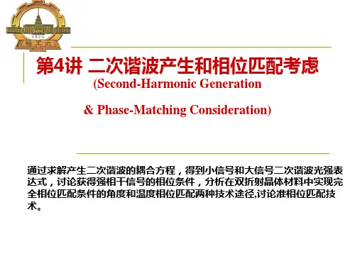
' 1 2 i kn P w 2 , z e z 2
E 1 z E 1 z i 2k1z 2 1 0 w 2 ;w1 , w1 e 2 2
简并度
辐射出二次谐波的电极化强度振幅:
2 1 2 P w2 , z 0 w2 ;w1 , w1 E 1 z E 1 z 2
2 2
2
d E2 z dz
w1deff
n2c
E1 z
2
w1deff 2 2 E 0 E z 1 2
n2c
利用积分公式:
dv 1 1 v a2 v 2 a tanh a
w1d eff E2 z E1 0 tanh E1 0 z n c 2 w1d eff E1 z E1 0 sech E1 0 z n2 c
(单色、均匀平面波)
基频波与介质相互作用产生的极化场:
' 1 2 ikn P ( t ) P wn , z e z e iwnt c .c . 2 2 1 1 ik1z iw1t 0 E 1 z e e c .c . E 1 z e ik1z e iw1t c .c . 2 2 激励出二次谐波的极化强度P(2w1)在频率内(不含时间项)的
考虑到电场强度和非线性极化强度是实数,应在光电场复 振幅和非线性极化场复振幅前乘以系数1/2,这样计算和实验 结果才能相一致.
1 ikn z iw n t E n ( z , t ) E n ( z )e e c .c . 2 NL NL ' 1 z iw n t P n ( z , t ) P n ( z )e ikn e c .c . 2
二次谐波的概念

二次谐波的概念
嘿,朋友!你知道啥是二次谐波不?这玩意儿听起来挺玄乎,其实没那么难理解。
咱先打个比方,就像唱歌。
你唱一个音,那是基频,可要是同时产生了一个频率是基频两倍的音,这多出来的就是二次谐波啦!
想象一下,电流在电线里流动,它可不是规规矩矩一直一个样的。
当它变化的时候,就可能产生各种谐波。
这二次谐波就像是电流队伍里冒出来的“调皮鬼”,它的出现会带来一些特别的影响。
比如说在电力系统里,二次谐波要是多了,那可就麻烦啦!就好像一个原本整齐有序的合唱团,突然有人跑调还特别大声,整个演出不就乱套了嘛!它会让电能质量下降,设备运行不稳定,甚至还可能损坏设备呢!
再拿电子设备来说,二次谐波的存在可能会干扰信号的传输,让你手机信号不好,或者电视画面模糊。
这多烦人呐!
那二次谐波是怎么产生的呢?这就好比一场化学反应。
有时候是因为非线性元件,就像一个任性的小孩,不按常理出牌,导致了二次谐波的出现。
还有的时候是因为电路中的磁性元件,它们就像爱捣乱的小精灵,一不留神就弄出了二次谐波。
对于工程师们来说,了解二次谐波那可是相当重要。
得像侦探一样,敏锐地发现它,准确地测量它,然后想办法把它的影响降到最低。
不然,设计出来的电路、系统可能就会出大问题。
总之,二次谐波虽然神秘,但只要我们用心去了解它,掌握它的规律,就能让它乖乖听话,为我们服务,而不是捣乱。
你说是不是这个
理儿?二次谐波,咱可不能小瞧了它,得好好研究,好好对付!。
倍频效应二次谐波精编版

倍频效应二次谐波集团企业公司编码:(LL3698-KKI1269-TM2483-LUI12689-ITT289-倍频现象的理论解释线性光学效应的特点:出射光强与入射光强成正比;不同频率的光波之间没有相互作用,没有相互作用包括不能交换能量;效应来源于介质中与作用光场成正比的线性极化。
非线性光学效应的特点:出射光强不与入射光强成正比(例如成平方或者三次方的关系);不同频率光波之间存在相互作用,可以交换能量;效应来源于介质中与作用光场不成正比的非线性极化。
倍频效应是非线性的光学效应,当介质在光波电场的作用下时,会产生极化。
设P是光场E在介质中产生的极化强度。
对于线性光学过程:P=ε0χE对于非线性光学过程:P可以展开为E的幂级数:ε=ε0χ(1)E+ε0χ(2)E2+ε0χ(3)E3+...ε0χ(ε)Eε+…其中:ε(1)=ε0χ(1)E,ε(2)=ε0χ(2)ε2,ε(3)=ε0χ(3)ε3,…,ε(ε)=ε0χ(ε)εε分别为线性以及2,3,…,n阶非线性极化强度。
χ(ε)为n阶极化率。
正是这些非线性极化项的出现,导致了各种非线性光学效应的产生。
而倍频效应,就是由其中的二阶极化强度ε(2)所导致产生的:ε−设光场是频率为ε、波矢为ε⃗⃗⃗⃗ 的单色波,即:ε=12εε−εε+c.c.ε0ε(2)ε2−则ε(2)=ε0χ(2)ε2中将出现项:142εε−2εε+c.c.该极化项的出现,可以看作介质中存在频率为2ε的振荡电偶极矩,它的辐射便可能产生频率为2ε的倍频光。
介质产生非线性极化:从微观上看,非线性是由原子、分子非谐性所造成的。
物质受强光作用后,电子发生位移x,具有位能V(x),对于无对称中心晶体,与电子位移+x和-x相对应的位能并不相等,即:V(+X)≠V(-x),因而位能函数V(x)应该包含奇次项:ε(ε)=12εε02ε2+13εεε3+⋯相应的,电子与核之间的恢复力为:ε=−ε(ε)ε=−(εεε2ε+εεε2+⋯)当D>0时,正位移(ε>0)引起的恢复力大于负位移(ε<0)引起的恢复力。
(推荐)二次谐波的产生及其解
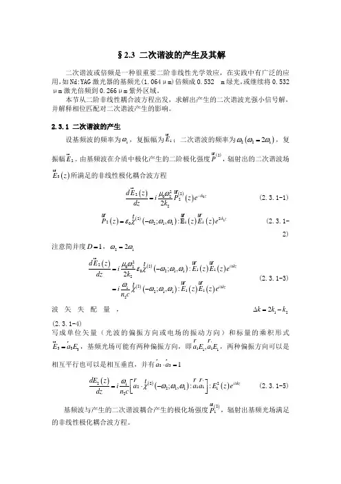
§2.3 二次谐波的产生及其解二次谐波或倍频是一种很重要二阶非线性光学效应,在实践中有广泛的应用,如Nd:YAG 激光器的基频光(1.064μm)倍频成0.532m 绿光,或继续将0.532μm 激光倍频到0.266μm 紫外区域。
本节从二阶非线性耦合波方程出发,求解出产生的二次谐波光强小信号解,并解释相位匹配对二次谐波产生的影响。
2.3.1 二次谐波的产生设基频波的频率为1ω,复振幅为1E u r;二次谐波的频率为()2212ωωω=,复振幅2E u r 。
由基频波在介质中极化产生的二阶极化强度()2P u r ,辐射出的二次谐波场()3E z u r所满足的非线性极化耦合波方程()()()222202222ik z d E z i P z e dz k μω-= u ru r (2.3.1-1) ()()()()()1222110211;,ik z P z z E z e εχωωω=-:E u r u r u r t (2.3.1-2)注意简并度1D =,212ωω=()()()()()()()()()22202110211221112112;,2;,i kzi kzd E z i E z E ze dz k i E z E z e n cμωεχωωωωχωωω∆∆=-:=-:u ru r u r t u r u r t (2.3.1-3)波矢失配量,122k k k ∆=-(2.3.1-4)写成单位矢量(光波的偏振方向或电场的振动方向)和标量的乘积形式333E a E =u r r,基频光场可能有两种偏振方向,即'1111,a E a E r r ,两种偏振方向可以是相互平行也可以是相互垂直,并有331a a ⋅=r r()()()()'222121121112;,i kz dE z i a a a E z e dz n c ωχωωω∆⎡⎤=⋅-::⎢⎥⎣⎦r r r t (2.3.1-5)基频波与产生的二次谐波耦合产生的极化场强度()21P u r ,辐射出基频光场满足的非线性极化耦合波方程。
电压偕波,的计算公式

智能建筑三A系统(设备自动化系统、办公自动化系统、通信自动化系统)中大量自动化设备需要高质量的电源,但同时其中相当数量的设备由于具有非线性负载特性,又是引发谐波畸变的扰动源。
因此分析引发谐波畸变的各类扰动源,并针对谐波畸变的危害,提出相应的防范措施,对智能建筑中三A系统的安全运行具有重要意义。
2 谐波分析依据国际电工委员会(IEC)在文献〔1〕中制定了单次谐波电压的兼容水平,即最大容许值。
当各次谐波电压低于文献〔1〕规定的限值时,总的谐波电压畸变不超过8%。
该规定兼顾了供电系统与制造商的共同利益。
在GB/T14549-93标准中规定:380V电网中各奇次谐波电压含有率限值为4%,各偶次谐波电压含有率限值为2%。
总的谐波电压畸变率允许值为5%。
以上均指相电压。
GB50174-93(电子计算机房设计规范)在电源质量分级中对谐波电压畸变率提出明确限值。
计算机房电源质量划分为A、B、C三级,允许谐波电压畸变率限值A级为3%~5%,B级为5%~8%,C级为8%~10%。
笔者认为智能建筑中其他自动化设备对电源质量的要求均可参考此规定限值。
总谐波畸变率THD是以基波为准的一个比值,用百分数表示,分为总电压谐波畸变率和总电流谐波畸变率。
总电流谐波畸变率计算公式如下:谐波电流畸变能对电压畸变产生很大影响,因此采取降低各类电气及电子设备的谐波电流至允许值,来满足低压配电网的兼容水平是行之有效的手段。
在分析谐波电流时,应注意多台设备产生的谐波电流具有一定规则的叠加性,也应考虑并非所有产生谐波的设备同时处于工作状态。
依据上述有关标准,在国内标准对智能建筑低压配电网总谐波电压畸变率限值尚无明确规定时,笔者认为可考虑将电源系统的总谐波电压畸变率限制在5%以下。
若超过5%应适当采取防范措施,以保证智能建筑三A系统的安全运行。
3 智能建筑内主要请波扰动源智能建筑中具有一定非线性负载特性的设备是产生谐波畸变的主要扰动源,可归纳为以下几类:①照明系统中的照明镇流器、调光设备(相位角控制器)。
谐波

二次谐波谐波产生的根本原因是由于非线性负载所致。
当电流流经负载时,与所加的电压不呈线性关系,就形成非正弦电流,从而产生谐波。
谐波频率是基波频率的整倍数,根据法国数学家傅立叶(M.Fourier)分析原理证明,任何重复的波形都可以分解为含有基波频率和一系列为基波倍数的谐波的正弦波分量。
谐波是正弦波,每个谐波都具有不同的频率,幅度与相角。
谐波可以I区分为偶次与奇次性,第3、5、7次编号的为奇次谐波,而2、4、6、8等为偶次谐波,如基波为50Hz时,2次谐波为lOOHz,3次谐波则是150Hz对于理想的电力系统,由于三相对称,因此负序和零序分量的数值都为零(这就是我们常说正常状态下只有正序分量的原因)。
当系统出现故障时,三相变得不对称了,这时就能分解出有幅值的负序和零序分量度了(有时只有其中的一种),因此通过检测这两个不应正常出现的分量,就可以知道系统出了毛病(特别是单相接地时的零序分量)。
下面再介绍用作图法简单得出各分量幅值与相角的方法,先决条件是已知三相的电压或电流(矢量值),当然实际工程上是直接测各分量的。
由于上不了图,请大家按文字说明在纸上画图。
编辑本段画图从已知条件画出系统三相电流(用电流为例,电压亦是一样)的向量图(为看很清楚,不要画成太极端)。
(1 ) 求零序分量(1 ) 求零序分量:把三个向量相加求和。
即A相不动,B 相的原点平移到A相的顶端(箭头处),注意B相只是平移,不能转动。
同方法把C相的平移到B相的顶端。
此时作A相原点到C相顶端的向量(些时是箭头对箭头),这个向量就是三相向量之和。
最后取此向量幅值的三分一,这就是零序分量的幅值,方向与此向量是一样的。
(2)求正序分量(2)求正序分量:对原来三相向量图先作下面的处理:A相的不动,B相逆时针转120度,C相顺时针转120度,因此得到新的向量图。
按上述方法把此向量图三相相加及取零序电流互感器三分一,这就得到正序的A相,用A相向量的幅值按相差120度的方法分别画出B、C两相。
什么是谐波?电力系统谐波怎么产生的?老司机给你科普一下!
什么是谐波?电力系统谐波怎么产生的?老司机给你科普一下!(1)谐波的含义在振动学里认为一个振动产生的波里具有一定频率的振幅最大的正弦波叫基波。
其他高于基波频率的小波就叫作谐波。
电力系统对谐波的定义:对周期性非正弦电量(电压或电流)进行傅立叶级数分解,除了得到与电网基波频率相同的分量,还得到一系列大于电网基波频率的分量,这部分电量称为谐波。
(基波及其表达式)(基波及2.3.4次谐波)(掺入2.3.4次谐波后的复合波)(2)谐波的产生电力系统是由发电、变电、输配电和用电这四个环节所组成的整体,每个环节均有可能产生谐波。
发电环节:略...变电环节:略...输配电环节:略...用电环节:用电系统中谐波主要是由非线性负载引起,由于正弦电压加压于非线性负载,基波电流发生畸变产生谐波。
主要非线性负载有UPS、开关电源、整流器、变频器、逆变器等。
三次谐波公式:复合波公式:(3)非线性设备含义简言之,设备中产生的电流波形是断续的或突变的,它不是一个可采用线性法则进行运算的连续函数,一般要采用傅里叶级数来描述它。
例如:上图为三相整流回路,整流后的电流波形为阶梯方波,右图是按傅里叶级数展开后的频谱,可以看出五次和七次谐波比例很高。
又如:上图为单相整流回路,整流后的电流波形为断续波形,右图是按傅里叶级数展开后的频谱,其中三次谐波比例很高。
(4)三次谐波电流的特殊性三次谐波电流主要是由单相非线性负载(如荧光灯,节能灯及镇流器等)产生的。
因其频率的特殊性,三次谐波在电网中性线上产生的后果尤为严重。
在三相电网中,基波各相的相位差为120°;而三次谐波相位差为360°。
由下图可见,各相线内的三次谐波电流在中性线上汇集时,其瞬时值是直接同相相加的,故中性线上的三次谐波电流一般为约为3倍的相线上的三次谐波电流,甚至会大于相线上的基波电流。
来源:继保小知识。
总谐波电流有效值计算公式
总谐波电流有效值计算公式总谐波电流有效值计算公式,这听起来好像有点复杂,但其实也没那么难理解。
咱们先来说说啥是谐波电流。
想象一下,电流就像一条流淌的小河,本来应该是平稳顺畅的,但有时候会出现一些“小波浪”,这些“小波浪”就是谐波电流。
那怎么计算总谐波电流的有效值呢?这就得用到专门的公式啦。
总谐波电流有效值的计算公式是:$I_{THD}=\sqrt{\sum_{n=2}^{\infty}I_{n}^{2}}$ ,这里的$I_{n}$表示第 n 次谐波电流的有效值。
我给您举个例子啊。
比如说在一个电路中,我们测得了 2 次谐波电流的有效值是 5A,3 次谐波电流的有效值是 3A,4 次谐波电流的有效值是 2A。
那按照公式来算,总谐波电流有效值就是:$\sqrt{5^{2} +3^{2} + 2^{2}} = \sqrt{25 + 9 + 4} = \sqrt{38}$ ,大概是 6.16A 。
我之前在一个工厂里做电路检测的时候,就碰到过谐波电流的问题。
那时候厂里的设备老是出故障,运转不太正常。
我们一开始都摸不着头脑,找了好久的原因。
后来经过仔细的检测和分析,发现就是谐波电流在捣乱。
当时为了算出总谐波电流有效值,可费了不少功夫呢。
拿着仪器测各种数据,在本子上密密麻麻地记录,然后再对照着公式一点点计算。
那场景,就跟打仗似的,紧张又刺激。
在实际应用中,准确计算总谐波电流有效值非常重要。
它能帮助我们判断电力系统的质量,及时发现问题,采取措施来减少谐波的影响,保障设备的正常运行。
比如说,通过安装滤波器,就可以有效地降低谐波电流,让电流这条“小河”重新变得平稳顺畅。
总之,虽然总谐波电流有效值计算公式看起来有点复杂,但只要我们掌握了方法,多结合实际情况去运用,就能轻松应对谐波电流带来的各种问题啦。
希望您也能顺利搞定这个知识点!。
高二物理竞赛课件二次谐波发生器
若引力非谐项为x2,则阻尼谐振子的运动 方程为:
mx 1x fx x 2 eE (10-22)
对于交变电场E=E0exp(2it),求解 x=x1exp(it)+x2exp(2it),并且x2<<1形 式的解,可得到:
5
x2
l (02
2
(e / m)3 E02 i1 / m)(02 42
二次谐波发生器
二次谐波发生器
大多数激光器的工作频率在红光到红外段 (如He-Ne激光器为11526Å;钕玻璃激光器 10600Å;红宝石激光器6973Å)。为了发射 可见光,需要产生谐波,其中以二次谐波 的能量最高。二次谐波的产生与非线性介 电效应相联系,但非线性介电效应与铁电 性并无必然联系。非线性是由于键力缺少 简谐性导致的。
9
对于中心对称晶体,电场符号的改变不影响 极化强度的大小,因此1=0。对二次谐波, P与E之间的关系为:
Pi (2) i1Ex2 i2 Ey2 i3 Ez2 (10-27) i4 Ey Ez i5 Ez Ex i6 Ex Ey
10
对于沿x方向传播的交变电场 E()=E0sin(t-kx),由频率为2的场所产 生的极化强度可写为:
2
因此,在电场的E[110]和E[1 10 ]两个分量之 间 出 现 相 位 滞 后 。 对 KDP 晶 体 , 109cm/V , 。 当 长 5cm 的 KDP 棒 , 施 加 电 场 是 2103V/cm,=7000Å,相位滞后为弧度。然 后可以对投射光进行分析和探测。
3
因此,如果在没有电场时没有光线通过探 测器,在有电场时,可能有光线通过。在 这一方面,可作为光断续器。如果施加交 变电场,由外加电场的频率可实现振幅调 制。对于KDP、石英和钛酸钡晶体,工作频 率大约在1010Hz。
谐波的定义及测试方法
供电系统谐波的定义是对周期性非正弦电量进行傅立叶级数分解,除了得到与电网基波频率相同的分量,还得到一系列大于电网基波频率的分量,这部分电量称为谐波。
谐波频率与基波频率的比值(n=fn/f1) 称为谐波次数。
电网中有时也存在非整数倍谐波,称为非谐波(Non-harmonics )或分数谐波。
谐波实际上是一种 干扰量,使电网受到“污染”。
目前公司常用测试输入电流谐波的仪器有TEK 系列示波器(可采用WAVESTAR 软件进行谐波分析),测试输出电压谐波的仪器有GW GAD-201G (失真仪)和TEK 系列示波器(可采用WAVESTAR 软件进行谐波分析)。
使用下面的方法计算信号的THD : () ++++++=272625242322211A A A A A A A THD 其中A 1是幅频特性中基波的幅值,而A 2 、A 3、A 4、A 5、……分别是2、3、4、5、……次谐波的幅值。
选取不同数量的谐波分量,可以计算出对应的THD 值。
采用WAVESTAR 软件进行分析可以得到完整谐波分析数据,下图为分析得出的柱型图,从图中可以针对各次谐波异常的状况采取相应的对策进行改善: Harmonic magnitude as a % of the fundamental amplitude0.0%0.7%1.5%2.2%3.0%3.7%4.4%5.2%5.9%6.6%7.4%8.1%Voltage:Current: Ch 1# Harmonics: 20Type: Current Magnitude波峰因数定义为交流信号峰值与有效值之比(峰均比),典型的波峰因数是: 正弦波:1.414;方波: 1;25%的占空比的脉冲:2 。
波峰因数(CREST FACTOR )的概念在UPS 行业是用来衡量UPS 带非线性负载的能力,对线性负载(R LOAD )而言,正弦波电流峰值Ipeak 与均方根值Irms 之比为1.414:1;在非线性负载(RCD LOAD )时,波峰因数则被认定为:在相同的有功功率条件下,非线性负载的电流峰值与非线性负载电流均方根值之比。