PFC控制器操作说明
中文PFC说明

中⽂PFC说明PFC3D命令说明(COMMON COMMAND REFERENCE)PFC3D是基于命令驱动模式(COMMAND-DRIVEN FORMAT)的软件,各种命令控制着程序的运⾏,这部分内容将介绍PFC3D软件的内嵌命令。
本说明⽂件译⾃PFC3D软件2.0版使⽤⼿册中的COMMAND REFERENCE部分,并补充了⼀些⼿册中没有的命令(如设置粘性阻尼、⽣成圆柱、螺旋壁⾯等,这些命令在更⾼版本的⼿册中有说明)。
命令说明的顺序没有采⽤原⼿册中按字母排序的⽅式,⽽是根据创建PFC3D 模型解决实际物理问题的⼀般过程,对相关命令加以说明。
PFC3D⼿册中COMMON COMMAND REFERENCE只对每个命令的格式和基本功能做了简单介绍,本说明⽂件对每个命令做了更详细的解释,为保持⽂件的可读性,对命令的详细解释都以附录形式给出。
本⽂件介绍了PFC3D的基本功能,对初学者有较⼤帮助,但要进⾏⾼级应⽤,还需清楚了解DEM和PFC3D相关功能的基本原理以及软件的结构等。
由于只关注使⽤PFC3D解决颗粒流的问题,涉及颗粒流的命令介绍的⽐较详细,⽽⽤于岩⼟⼯程等其他领域的命令,由于关注很少且专业知识缺乏,只是不求甚解。
0.关于命令格式的说明:PFC3D中每个命令基本包含3部分:命令名、必需关键词和可选关键词。
本说明⽂件中,命令名和必需关键词写在第⼀⾏,尖括号表⽰该命令具有可选关键词,罗列于命令名的下⼀⾏次级列;带参数的关键词,参数紧随关键词之后⽤加粗斜体表⽰。
名字较长的“命令”和“关键词”,PFC3D允许不写出全部字母,只需简写前⾯的⼀些字母,最短可简写名(即PFC3D能识别的最短简写“命令”和“关键词”名)⽤加粗字体表⽰。
例如命令:BALL rad r…hert z …id idx xy yz z说明:命令名为BALL的命令,具有必需关键词rad(参数r)和hert z、id、x、y、z等可选关键词。
高压无功补偿控制器-PFC-H说明书
8.输出路数: 1-12可编程
9.投切延时:1S-999S可编程
10.投切方式:先投先切,先投后切等投切方式。
11.保存功能:所有编程的参数和模式,保存在一个非易失存储器中
12.谐波检测:可检测谐波保护功能。
13.电源: AC/DC 100~220V
-6-
联系电话:0755-23351975
14.重量:1.0Kg(净重)
电容器过流速断保护1设置:
出厂预设:关闭 用途:电容器过流保护
范围:5-150%(对应为0.25-7.5A) 步长:1%
以此类推2,3,4路
电容器保护延时:
出厂预设:40S 用途:过流保护动作延时
C/K变比
范围:1S—999S 步长:1
显示编程设定的 C/k 值,可按照以下公式计算 C/k 的建议设置,直接查阅下列图表。
以此类推:PFC-H 电保持(带保护)接线图
-5-
联系电话:0755-23351975
四.功 能
官方网站:
4.1测量功能
控制器能测量电压、电流、功率因数、有功、无功、谐波、保护状态、频率等多种电量,自动实现 温漂、零漂的校正。
4.2 补偿功能
在精确测量的基础上,控制器全面支持对系统的补偿功能,补偿响应快,控制准确,支持循环投切、 8421编码等多种补偿方式。
切除。
! 特别提示:
在配电系统负荷小时,不可动手强行投入较多电容。
6.2基本参数设置
1.系统上电后进入主菜单,延时10秒,进入自动运行状态
自动 手动 设置
! 特别提示:如首次使用,需对设备编号、变比、电容等参数进行设置。
液晶显示屏
显示设置参数/工作状态及标志/电网有关参数。 背光有自动自动关闭(按任意键激活背光),或常亮2种形式。
STNRGPF12数字控制器的2 kW双通道交错PFC使用说明书

IntroductionThe STEVAL-IPFC12V1 2 kW interleaved PFC kit is based on the STNRGPF12 digital controller and consists of a power board,control board and adapter board. The STNRGPF12 is a digital configurable ASIC developed by STMicroelectronics, which can drive up to two channels in an interleaved PFC for industrial applications.The STNRGPF12 digital controller on the control board implements mixed signal (analog/digital) average current mode control in CCM at fixed frequency. The analog section ensures cycle-by-cycle current regulation, while digital control manages the non-time-critical operations. You can use the eDesignSuite software available on the ST website to configure the STNRGPF12 to satisfy the specifications of each interleaved PFC.Figure 1.STEVAL-IPFC12V1 evaluation kit with power, control and adapter boardsHow to use the 2 kW two-channel interleaved PFC based on the STNRGPF12digital controllerUM2537User manualSafety instructions 1Safety instructionsDanger:The evaluation board uses voltage levels that can cause serious injury and even death.Do not touch any components immediately after disconnecting the input power supply as thecharged capacitors need time to discharge.Due to the high power density, board components and heat sinks can become very hot and causesevere burns when touched.This board is intended for use by skilled technical personnel who are suitably qualified and familiar with theinstallation, use and maintenance of power electronic systems. The same personnel must be aware of and mustapply national accident prevention rules.The electrical installation shall be completed in accordance with the appropriate requirements (e.g., cross-sectional areas of conductors, fusing, and GND connections).STEVAL-IPFC12V1 evaluation kit overview 2STEVAL-IPFC12V1 evaluation kit overviewFigure 2. STEVAL-IPFC12V1 block diagram1.I/O measurement signals2.Analog circuitry3.Power stages4.The STEVAL-IPFC12V1 implements mixed signal (analog/digital) control, combining the flexibility of aprogrammable high end digital solution with the responsiveness and accuracy of analog componentry. The innercurrent loop consists of an analog proportional-integral (PI) compensator that ensures the highest possiblebandwidth and cycle-by-cycle regulation. The outer voltage loop is performed by a digital PI controller with fastdynamic response.2.1Board featuresThe 2 kW interleaved PFC evaluation kit features:• A modular design with the following separate boards:–STEVAL-IPFC12P1 power board–STEVAL-IPFC12C1 control board–STEVAL-IPFC01A1 adapter board•2-channel interleaved PFC•Input voltage range: 90 to 265 V AC (50 or 60 Hz)•Maximum output power: 2 kW at 230 V AC; 1 kW at 115 V AC;•Output voltage: 400 V•Fixed frequency average current mode control and CCM operation•Mixed-signal, semi-digital approach•Programmable phase shedding•Cooling System management•Programmable fast overcurrent and thermal protection•Digital inrush current limiter function performed with relay•Soft startup and burst mode management•Load current and input voltage feed forward•Channel current balance functionBoard features•Two status LEDs to signal nominal and fault conditions•Browser GUI tool (eDesignSuite) for driver customization•Serial communication port for–STNRGPF12 programming–PFC parameter monitoring3How to use the STEVAL-IPFC12V1 evaluation boardTo perform functional and efficiency testing, you need the following equipment:•Programmable AC source with power > 2 kW •DC electronic load or load resistor > 2 kW •Power analyzer •Digital oscilloscopeThe STEVAL-IPFC12V1 board can be tested up to 2 kW at 230 V RMS and 1 kW at 115 V RMS , in a frequency range between 47 and 63 Hz.Note:Any load or passive oscilloscope probe must be isolated from the input source of the PFC.3.1How to connect and start the STEVAL-IPFC12P1 power boardStep 1.Insert the STEVAL-IPFC12C1 control board in connector J301 on the STEVAL-IPFC12P1 power board.Step 2.Connect one of the following AC supplies to the J100 connector on the STEVAL-IPFC12P1 power board:–230 V at 50 Hz –115 V at 60 HzFigure 3.STEVAL-IPFC12P1 AC supply connectionHow to use the STEVAL-IPFC12V1 evaluation boardStep 3.Connect the load wires to the output terminals on J300 of the STEVAL-IPFC12P1 power board.The actual load (electronic dc load, load resistors, inverter, etc.) must remain disconnected until thesoft startup sequence has completed.The correct polarity is indicated on the board.Figure 4. STEVAL-IPFC12P1 DC output connectionStep 4.Supply one of the following input voltage and frequency ranges while no load is connected on the output:–185 – 265 V AC at 47 - 53 Hz–90 – 140 V AC at 57 – 63 Hz3.1.1STEVAL-IPFC12P1 power board startup sequence1.The appropriate AC input voltage is applied under a no load condition.2.When the input voltage rises above 60 V, the auxiliary power supply starts and generates the auxiliaryvoltages (15 V DC and 5 V DC) for the drivers and the signal conditioning circuitry.3.Once the auxiliary voltages are nominal, the inrush current limiter phase begins by charging the outputcapacitor until the DC voltage reaches the peak input voltage. The current is limited by the SCRs Q102 andQ103.Figure 5. STEVAL-IPFC12P1 input section4.The STNRGPF12 then checks for any output current flow:–If there is no current, the STNRGPF12 closes the contacts of a mechanical relay in parallel with resistor R101.–If any current is detected, the STNRGPF12 will keep the relay contacts on R300 open (so the board cannot start) until the current falls to zero.5.After the inrush limiter phase, the soft startup procedure is activated and the output voltage rises up to 436VDC, at which point the PFC enters burst mode to regulate the output voltage between 416 and 436 VDC.6.The green LED D2 on the control board indicates when the sequence has finished and the PFC is ready forthe load to be connected.7.Once you connect the load:–the output voltage is regulated to 400 V ±2 V.–for 185 – 265 V 50 Hz mains, the maximum output power is 2000 W –for 90 – 140 V 60 Hz mains, the maximum output power is 1000 W4PFC controller customization with eDesign SuiteThe eDesignSuite suite software tool developed by STMicroelectronics helps you configure ST products powerconversion applications. You can use it to customize the PFC controller for a specific application: you start byentering the main specifications for your design and then generate an automatic design or follow a sequentialprocess to build a highly customized design.Figure 6. PFC specificationsFigure 7. PFC step-by-step designRELATED LINKSSee RM0446 for details on how to use eDesignSuite to generate specialized firmwareStatus LEDs and fault conditions 5Status LEDs and fault conditionsThe STEVAL-IPFC12C1 control board has the following status LEDs:• a green LED connected to STNRGPF12 pin 15 (PFC_OK)• a red LED connected to STNRGPF12 pin 14 (PFC_FAULT)5.1Normal operationDuring normal operation, the green LED (D1) on the STEVAL-IPFC12C1 control board remains lit to indicate thatthe PFC is operating under allowable conditions.5.2Fault conditionsWhen a fault is detected, the red LED (D2) on the STEVAL-IPFC12C1 control board lights up and the green LED(D1) turns off. The device stops all switching activities and turns off the fan.After a fault condition, the board must be reset by switching off the AC input voltage and discharging the outputcapacitors.Note:Warning: Do not short the output terminals to discharge the capacitors as the high discharge current may damage the output current sensing circuitry.The following conditions will trigger a fault protection:• A mismatch between frequency and voltage or highly distorted input voltage waveforms that inhibit frequency measurement. For example, if the input voltage is 230 V RMS but the mains frequency is 60 Hz, orif the input voltage is 115 V RMS and the mains frequency is 50 Hz.•Overcurrent condition on at least one PFC channel. This protection prevents PFC inductor saturation.•Overvoltage protection on output voltage if the output voltage exceeds 440 V DC•Overvoltage protection on input voltage:–for 115 V nominal supply: above 140 V–for 230 V nominal supply: above 265 V•Over-temperature protection when the ambient temperature of the board exceeds the threshold setting. 5.3Wait conditionsIn addition to the conditions that trigger PFC_OK and PFC_FAULT, there are other conditions that are indicatedwith both LEDs are off:•Undervoltage condition on the output when the DC bus voltage falls below 340 V.•Undervoltage condition on input when the input rms voltage falls below 90 V at 60 Hz or 185 V at 50 Hz.•Input voltage dropout when the input voltage signal disappears for more than 25 ms.Under these conditions, the STNRGPF12 will drive both LEDs on the control board off and will wait until theconditions have cleared before repeating the startup sequence.UM2537STEVAL-IPFC12V1 schematic diagrams 6STEVAL-IPFC12V1 schematic diagrams6.1STEVAL-IPFC12P1 power board schematicsFigure 8.STEVAL-IPFC12P1 schematic - input sectionSCR SWINPUT__2701SWSW270___SCR R107V 2_R104UM2537STEVAL-IPFC12P1 power board schematicsFigure 9. STEVAL-IPFC12P1 schematic - auxiliary power supplyUM2537STEVAL-IPFC12P1 power board schematicsFigure 10. STEVAL-IPFC12P1 schematic - boost interleaving sectionCON40AC31411k10k UM2537STEVAL-IPFC12P1 power board schematics6.2STEVAL-IPFC12C1 control board schematicFigure 11. STEVAL-IPFC12C1 schematicUM2537STEVAL-IPFC12C1 control board schematic6.3STEVAL-IPFC01A1 adapter board schematicFigure 12.STEVAL-IPFC01A1 schematicJ 401CON6STEVAL-IPFC01A1 adapter board schematic7STEVAL-IPFC12V1 bill of materialsTable 1. STEVAL-IPFC12V1 bill of materials7.1STEVAL-IPFC12P1 power board bill of materialsTable 2. STEVAL-IPFC12P1 bill of materials7.2STEVAL-IPFC12C1 control board bill of materialsTable 3. STEVAL-IPFC12C1 bill of materials7.3STEVAL-IPFC01A1 adapter board bill of materialsTable 4. STEVAL-IPFC01A1 bill of materialsRevision historyTable 5. Document revision historyContentsContents1Safety instructions (2)2STEVAL-IPFC12V1 evaluation kit overview (3)2.1Board features (3)3How to use the STEVAL-IPFC12V1 evaluation board (5)3.1How to connect and start the STEVAL-IPFC12P1 power board (5)3.1.1STEVAL-IPFC12P1 power board startup sequence (6)4PFC controller customization with eDesign Suite (8)5Status LEDs and fault conditions (10)5.1Normal operation (10)5.2Fault conditions (10)5.3Wait conditions (10)6STEVAL-IPFC12V1 schematic diagrams (11)6.1STEVAL-IPFC12P1 power board schematics (12)6.2STEVAL-IPFC12C1 control board schematic (15)6.3STEVAL-IPFC01A1 adapter board schematic (16)7STEVAL-IPFC12V1 bill of materials (17)7.1STEVAL-IPFC12P1 power board bill of materials (17)7.2STEVAL-IPFC12C1 control board bill of materials (22)7.3STEVAL-IPFC01A1 adapter board bill of materials (25)Revision history (26)List of figuresFigure 1. STEVAL-IPFC12V1 evaluation kit with power, control and adapter boards (1)Figure 2. STEVAL-IPFC12V1 block diagram (3)Figure 3. STEVAL-IPFC12P1 AC supply connection (5)Figure 4. STEVAL-IPFC12P1 DC output connection (6)Figure 5. STEVAL-IPFC12P1 input section (6)Figure 6. PFC specifications (8)Figure 7. PFC step-by-step design (9)Figure 8. STEVAL-IPFC12P1 schematic - input section (12)Figure 9. STEVAL-IPFC12P1 schematic - auxiliary power supply (13)Figure 10. STEVAL-IPFC12P1 schematic - boost interleaving section (14)Figure 11. STEVAL-IPFC12C1 schematic (15)Figure 12. STEVAL-IPFC01A1 schematic (16)List of tablesTable 1. STEVAL-IPFC12V1 bill of materials (17)Table 2. STEVAL-IPFC12P1 bill of materials (17)Table 3. STEVAL-IPFC12C1 bill of materials (22)Table 4. STEVAL-IPFC01A1 bill of materials (25)Table 5. Document revision history (26)IMPORTANT NOTICE – PLEASE READ CAREFULLYSTMicroelectronics NV and its subsidiaries (“ST”) reserve the right to make changes, corrections, enhancements, modifications, and improvements to ST products and/or to this document at any time without notice. Purchasers should obtain the latest relevant information on ST products before placing orders. ST products are sold pursuant to ST’s terms and conditions of sale in place at the time of order acknowledgement.Purchasers are solely responsible for the choice, selection, and use of ST products and ST assumes no liability for application assistance or the design of Purchasers’ products.No license, express or implied, to any intellectual property right is granted by ST herein.Resale of ST products with provisions different from the information set forth herein shall void any warranty granted by ST for such product.ST and the ST logo are trademarks of ST. For additional information about ST trademarks, please refer to /trademarks. All other product or service names are the property of their respective owners.Information in this document supersedes and replaces information previously supplied in any prior versions of this document.© 2020 STMicroelectronics – All rights reserved。
PFC-12控制器说明书

数)进行修改;操作“确定”键:操作生效;操作“菜单”键:返回上一级菜单。
各设置项下的参数设置内容为:
“设备设置”包括:设备编号、变比、有功电度、无功电度。如图 13 所示。 该界面中所有参数均按位设置。
“补偿设置”包括:投入系数、切除系数、投入延时、切除延时。如图 14 所 示。
“电容设置”包括:设备中△型、Y 型电容器的组数、容量及电容器的配置方 案。如图 15 所示。
Http:
一、产品概述:
PFC 无功补偿控制器采用全数字化设计、交流采样、四象限分析,人机界面 为 12864 点阵大屏幕液晶显示器,监测配电变压器、配电线路运行状态和补偿电网 无功。集实时数据采集、历史数据存储、通讯、无功补偿、谐波分析、故障报警、 配电综合监测等功能于一体的新型配电监控设备,适用于三相四线制配电网的综合 监测及无功补偿控制。也可单独作为配电负荷综合监测仪使用。具有 232/485 通讯 接口;支持 GPRS 网络远程通讯;支持短距离(1000 米以内)无限抄表,配套手持式 数据抄表器。可以直接连接电脑,进行联机操作。
广州阿珂法电器 Tel:020-82029012 / 82051945 Fax:82051079
Http:
4.2 电压信号线兼作监控终端电源输入,所以安3 电流信号线宜选用大于 1.5MM 平方的单股铜导线,且导线尽可能短。 4.4 带电采集、设置数据时,均不得接触带电部分、以确保人身设备安全。
图 17
图 18
按键操作说明: 在设置界面下(图 12 所示),操作“▲”键、“▼”键:可选
择不同的修改设置项,在图 13——图 18 所示的界面中,对当前的参数(反显的参
广州阿珂法电器 Tel:020-82029012 / 82051945 Fax:82051079
NCP1608中文
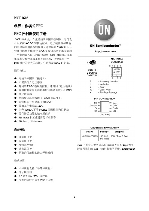
NCP1608临界工作模式PFCPFC控制器使用手册NCP1608 是一个主动的功率因素控制器,专门设计用来在AC-DC转换适配器,电子镇流器和其他的中等功率的离线转换器(通常功率350W以下)。
它使用临界工作模式(CrM)保证高的功率因素和一个宽的输入电压和输出功率。
NCP1608通过内部集成安全特性来最小化外围回路,使他成为一个PFC设计的优秀的选择。
它通常是SOIC-8 封装。
通用特性:●高的功率因素(接近1)●不需要输入电压感应●封闭的PWM逐周期控制开通时间(电压模式)●宽的控制范围为高功率应用噪音免疫(>150W)●跨导放大器●高精度电压参考源(1.6%任何温度下)●非常低的开启电压(<35uA)●低的工作电流(2.1mA)●上升500mA/下降800mA图腾柱结构门驱动●带有滞后功能的低电压保护●Pin to pin和工业通用的标准兼容●PB free ,Halide free安全特性●过电压保护●低电压保护●反馈悬空保护●过电流保护●精准的可编程的最大开通时间经典应用●固体照明设备(半导体照明)●电子镇流器●AC适配器,TV,监控器●所有的离线的需要PFC的应用Tape上有卷的说明信息包括部分方向和Tape大小,请参考我们的tape上的包装说明手册,BRD8011/D图1经典应用图2 内部结构框图表格1:pin针功能说明超过最大额定值可能损坏芯片。
最大额定值仅仅是加的电压,在正常工作中以上情况不能适用。
长期的暴漏于以上情况会影响芯片的信赖性。
1.这个芯片包括静电放电(ESD)保护达到以下测试:Pin1-8:人体模型超过2000V 每个JEDEC 标准JESD22-A114E机器模型办法200V 每个JEDEC 标准JESD22-A115A 。
表格3 电气特性V FB=2.4V,V Control = 4 V, Ct = 1 nF, V CS = 0 V, V ZCD = 0 V, C DRV = 1 nF, V CC = 12 V,除非另有说明。
PFC-02功率因数自动控制器使用说明
PFC-02功率因数自动控制器使用说明注意事项:1、PFC-02功率因数控制器不能与PFC-01控制器互换;2、PFC-02功率因数控制器的C2和C3接线端子应接到发电机的C2 和C3上,绝对不能短路,不能接到发电机的A1和A3上,否则可能造成控制器的损坏;3、当不用外部调压电位器时,应将发电机AVR板上的S3开关闭合,即在上方位置;4、交流电压信号为两相相电压和另外一相线电流;5、PFC-02适用于1FC6发电机。
一、简介由于电网电压的变化及发电机组有功功率的变化,机组的功率因数时常变化,功率因数自动控制器,就可以根据功率因数的变化情况输出一控制信号给发电机的电压调节器AVR,从而达到自动调节发电机输出无功功率的目的,即使功率因数保持恒定。
该装置的功率因数自动调节功能只适用于与电网并联运行的发电机组,对于并车运行的机组,可设定其工作在手动方式,从而实现机组之间无功功率的均匀分配,即功率因数的手动调整。
二、主要技术参数工作电源:22VDC~28VDC功率因数调节范围:0.5-1.0(滞后)功率因数调整适用范围:5%-100%机组额定电流功率因数控制精度:1~4%,可随意设定发电机交流电压输入信号:380VAC发电机交流电流输入信号:0~5A三、主要特点1、智能化:目标功率因数,控制精度,控制速度等多个参数可任意设定。
2、人性化:当手动进行控制时,若“增加”或“减少”状态保持2秒以上时,进行快速控制。
3、测量精度高,且与信号线的接线顺序无关:本控制器采用两相相电压和另外一相电流的测量方法,测量的功率因数只与发电机组的实际功率因数有关,而与接线方式无关,也就是说,更换电压的接线顺序或者电流取样的顺序不影响测量值;该方法测量准确,精度高。
四、参数设定1、目标功率因数的设定a)按“设定/保存”按键,直至显示“SET”字样;b)“SET”显示完毕之后,随后显示目前已设定的功率因数值;c)按“增加”键,增加设定功率因数值;d)按“减少”键,减少设定功率因数值;e)功率因数设定范围为0.5~1.0,超出范围时,显示“ERR”,并退出设定参数程序,不保存设定值;f)设定完毕后,按“设定/保存”按键进行保存。
Richtek RT7313GS PFC控制器商品说明书

RT7313GSRT7313Copyright © 2016 Richtek Technology Corporation. All rights reserved. is a registered trademark of Richtek Technology Corporation.DS7313-01 July 20161PFC Controller with Critical Conduction ModeGeneral DescriptionThe RT7313 is an active Power Factor Correction (PFC) controller with critical conduction mode (CRM) operation that is designed to meet line current harmonic regulations for the applications of AC/DC adapters, electronic ballasts and medium off-line power converters (<300W). The CRM and Feed-Forward schemes provide near unity power factor across a wide range of input voltages and output powers.The totem-pole gate driver with 600mA sourcing current and 800mA sinking current provides powerful driving capability for power MOSFET to improve conversion efficiency. The RT7313 features an extra low start-up current (≤20μA) and supports a disable function to reduce power consumption in standby mode, which makes it easy to comply with energy saving regulations such as Blue Angel, Energy Star and Energy 2000.This controller integrates comprehensive safety protection functions for robust designs including input under-voltage lockout, output over-voltage protection, under-voltage protection and cycle-by-cycle current limit.The RT7313 is a cost-effective solution for PFC power converter with minimum external components. It is available in the SOP-8 package.Features● Critical Conduction Mode (CRM) Operation ● Constant On-Time Control (Voltage Mode) ● Near Unity Power Factor● Ultra Low Start-up Current (≤20μA)● Input Voltage Feed-Forward Compensation ● Wide Supply Voltage Range from 12V to 25V ● Totem Pole Gate Driver with 600mA/-800mA ● Maximum Frequency Clamping (120kHz) ● DCM THD Optimization ● Fast Dynamic Response● Light Load Burst Mode Operation ● Disable Function● Maximum/Minimum On-Time Limit ● Cycle-by-Cycle Current Limit● Output Over-Voltage Protection (OVP) ● Under-Voltage Lockout (UVLO) ●RoHS Compliant and Halogen FreeApplications● Electrical Lamp Ballast ● LED Lighting●AC/DC Adapter/Charger for Desktop PC, NB, TV, Monitor, Etc.●Entry-Level Server, Web ServerSimplified Application CircuitPSR ConverterOUT +OUT -SSR ConverterOUT +OUT -OUT1OUT2RT7313Copyright © 2016 Richtek Technology Corporation. All rights reserved. is a registered trademark of Richtek Technology Corporation. DS7313-01 July 20162Ordering InformationRT7313G : Green (Halogen Free and Pb Free)Note :Richtek products are :④ RoHScompliant and compatible with the currentrequirements of IPC/JEDEC J-STD-020.④ Suitable for use in SnPb or Pb-free soldering processes.Marking InformationRT7313GS : Product Number YMDNN : Date CodePin Configuration(TOP VIEW)INV COMPFF CSVDD GD ZCDGNDSOP-8Functional Pin DescriptionFunctional Block DiagramRT7313Copyright © 2016 Richtek Technology Corporation. All rights reserved. is a registered trademark of Richtek Technology Corporation.DS7313-01 July 20163OperationCritical Conduction Mode (CRM)The Critical Conduction Mode is also called Transition Mode or Boundary Mode. Figure 1 shows the CRM operating at the boundary between Continuous Conduction Mode (CCM) and Discontinuous Conduction Mode (DCM).In CRM, the power switch turns on immediately when the inductor current decreases to zero. The CRM is the preferred control method for medium power (<300W) applications due to the features of zero current switching and lower peak current than that in DCM.Figure 1. Inductor Current of DCM, CRM and CCM Constant On-Time Voltage Mode ControlFigure 2 shows a typical flyback converter. When the MOSFET turns on with a fixed on-time (t ON ), the inductor current can be calculated by the following equation (1).TX1OUTV OUTFigure 2. Typical flyback ConverterIN L_PK ON PFCVI = t (1)L⨯If the input voltage is a sinusoidal waveform and rectified by a bridge rectifier, the inductor current can be expressed with equation (2). When the converter operates in CRM with constant on-time voltage modecontrol, the envelope of inductor peak current will follow the input voltage waveform with in-phase. The average inductor current will be half of the peak current shown as Figure 3. Therefore, the near unity power factor is easy to be achieved by this control scheme.||||IN_pk ONL_pk PFCV sin θt I sin θ=(2)L ⨯⨯⨯I L_PK I Q1I in_avg I DOUTPeak Inductor Current MOSFET Current Average Input Current Output Diode CurrentV IN Input Voltage V Q1_GATE MOSFET Gate VoltageFigure 3. Inductor Current of CRM with ConstantOn-Time Voltage Mode Control Under-Voltage LockoutThe controller will be enabled when VDD exceeds V ON_TH (16V typ.) and disabled when VDD decreases lower than V OFF_TH (9V typ.).The maximum VDD voltage is set at 27V typically forover-voltage protection shown as Figure 4. An internal 29V zener diode is also used to avoid over voltage stress for the internal circuits.When the VDD is available, the precise reference is generated for internal circuitries such as Error Amplifier, Current Sense, OVP, UVP. The internal reference equips with excellent temperature coefficient performance so that the RT7313 can be operated in varied environments.RT7313Copyright © 2016 Richtek Technology Corporation. All rights reserved. is a registered trademark of Richtek Technology Corporation.DS7313-01 July 20164Figure 4. VDD and UVLOFeedback Voltage DetectionFigure 5 shows the feedback voltage detection circuit. The INV pin is the inverting input of the Error Amplifier with 1.5V reference voltage. Over-voltage protection is provided with threshold voltage 1.65V. If the INV voltage is over 1.65V, the gate driver will be disabled to prevent output over voltage condition or feedback open condition. Although the INV is an input pin with high impedance, it is suggested that the bias current of the potential divider should be over 30µA for noise immunity.Figure 5. Feedback Voltage DetectionTransconductance Error AmplifierThe RT7313 implements transconductance error amplifier with non-linear GM design to regulate the Flyback output voltage and provide fast dynamic response. The transconductance value is 100µA/V in normal operation. When the INV voltage increases over 1.65V or decreases under 1.35V, the output of error amplifier will source or sink 1.5mA(typ.) maximum current at COMP pin respectively shown as Figure 6. Thus, the non-linear GM design can provide fast response for the dynamic load of PFC converters even though the bandwidth of control loop is lower than linefrequency.Figure 6. Non-linear GMFeed-Forward CompensationThe FF pin is an input pin with high impedance to detect the line input voltage shown as Figure 7. A proper voltage divider should be applied to sense the line voltage after bridge diode rectifier. Since the FF voltage is proportional to the line input voltage, it provides a feed-forward signal to compensate the loop bandwidth for high line and low line input conditions.Figure 7. FF Detection CircuitThe constant on-time, t ON , can be derived from the following equations.()2)ON IN_pk ON IN IN_pk L_pk L_pk ONS PFC2IN_pk IN_pk ON ON IN IN_pk ON ON PFC S PFC SIN PFCON IN_pk S V t1P V I I t 4t L V (V t t 11P V t t 4L t 4L t 4P L t (3)t V t =⨯⨯⨯=⨯=⨯⨯⨯⨯=⨯⨯⨯⨯⨯⇒=⎛⎫⨯ ⎪⎝⎭RT7313Copyright © 2016 Richtek Technology Corporation. All rights reserved. is a registered trademark of Richtek Technology Corporation.DS7313-01 July 20165In RT7313, the t ON is implemented by a constant current charging a capacitor till V COMP threshold voltage is reached. Therefore, the t ON is a function of V COMP .()ramp COMP D ON ramp C V V t = 4I ()⨯-Then, the V COMP can be derived from equation (3) and (4).()()()22ramp COMP D IN PFCramp ON IN_pk S ramp IN PFCCOMP D rampON IN_pk S C V V 4P L I t V t I 4P L V + V (5)C t V t ⨯-⨯⨯=⎛⎫⨯ ⎪⎝⎭⨯⨯=⨯⎛⎫⨯ ⎪⎝⎭According to equation (5), the V COMP is reversely proportional to the input voltage so that the V COMP has a large variation for the change of line voltage between high and low input voltages. This variation will impact t ON , Burst mode entry level and loop bandwidth. In order to compensate the variation, the I ramp is designed to be proportional to the input voltage shown as equation (6).()2ONramp IN_pk FF ramp S2ON FF2IN_RMS ramp FF1FF2S 2FF2ramp IN PFC FF1FF2Comp D 2rampt I (V )k V gm t t R = k V gm (6)R + R t V 8gm P L R + R V (FF) + V C π=⨯⨯⨯⎡⎤⎛⎫⨯⨯⨯⎪⎢⎥⎝⎭⎣⎦⎛⎫⨯⨯⨯⨯ ⎪⎝⎭=⨯ (7)in which k, gm ramp , C ramp , and V D are fixed parameters in the RT7313, and the typical values are : k = 0.5, gm ramp = 10μA/V, C ramp = 4.5pF, and V D = 1V. Ramp GeneratorThe RT7313 provides constant on-time voltage mode control to achieve near unity power factor for the CRM Flyback converters. Figure 8 shows the Ramp Generator with Feed-Forward compensation and THD optimization circuit for the constant on-time operation.Figure 8. Ramp GeneratorThe charging current of ramp generator is modulated following the squared FF voltage with line voltage compensation and the THD optimization scheme is implemented to compensate the harmonic distortion. ZCD and Enable FunctionIn CRM operation, when the power switch turns on, the inductor current increases linearly to the peak value. When the power switch turns off, the inductor current decreases linearly to zero. The zero current can be detected by the ZCD pin with the auxiliary winding of Flyback inductor.Figure 9 and Figure 10 show the ZCD block diagram and related waveforms. The ZCD block diagram provides zero current detection, voltage clamp and shutdown control functions. When the inductor current decreases to zero, the auxiliary winding voltage will turn from high to low. Once the ZCD voltage decreases to the threshold V ZCDT (1V, typ.), the controller will generate a signal for gate driver. The hysteresis voltage between the threshold V ZCDA (1.6V, typ.) and V ZCDT is designed to avoid mis-triggering. In order to prevent over voltage stress, the ZCD pin voltage is clamped at V ZCDH (4.8V, typ.) if the input voltage is too high from the auxiliary winding and the ZCD pin voltage is clamped at V ZCDL (0.6V, typ.) if the input voltage is lower than V ZCDL .RT7313Copyright © 2016 Richtek Technology Corporation. All rights reserved. is a registered trademark of Richtek Technology Corporation. DS7313-01 July 20166R ZCDFigure 9.ZCD Block DiagramThe RT7313 provides shutdown function to save power consumption in standby mode. When the ZCD pin is pulled lower than 250mV, the gate driver will be turned off and operate in standby mode with low quiescent current less than 600µA. Once the ZCD pin is released, the controller will be activated.The RT7313 also provides ZCD time-out detection function. If the controller runs at maximum frequency and there is no ZCD signal being detected after 4µs delay time, the PWM will be turned on for ZCD time-out detection.V V I V V V VFigure 10. ZCD Related Waveforms.RT7313Copyright © 2016 Richtek Technology Corporation. All rights reserved. is a registered trademark of Richtek Technology Corporation.DS7313-01 July 20167Absolute Maximum Ratings (Note 1)● Supply Voltage, VDD --------------------------------------------------------------------------------------------- -0.3 to 30V ● Gate Driver Output, GD ------------------------------------------------------------------------------------------ -0.3V to 20V ● Other Pins ----------------------------------------------------------------------------------------------------------- -0.3V to 6V ●Power Dissipation, P D @ T A = 25°CSOP-8 ------------------------------------------------------------------------------------------------------------------ 0.625W ●Package Thermal Resistance (Note 2)SOP-8, θJA ------------------------------------------------------------------------------------------------------------ 160°C/W ● Junction Temperature -------------------------------------------------------------------------------------------- 150°C ● Lead Temperature (Soldering, 10 sec.) ------------------------------------------------------------------------ 260°C● Storage Temperature Range ------------------------------------------------------------------------------------- -65°C to 150°C ● ESD Susceptibility (Note 3)●HBM (Human Body Model) --------------------------------------------------------------------------------------- 2kVRecommended Operating Conditions (Note 4)● Supply Voltage, VDD ----------------------------------------------------------------------------------------------- 12V to 25V ●Junction Temperature Range ------------------------------------------------------------------------------------ -40°C to 125°CElectrical Characteristics(V DD = 15V, T A = 25︒C, unless otherwise specification)RT7313Copyright © 2016 Richtek Technology Corporation. All rights reserved. is a registered trademark of Richtek Technology Corporation. DS7313-01 July 20168Note 1. Stresses beyond those listed “Absolute Maximum Ratings ” may cause permanent damage to the device. These arestress ratings only, and functional operation of the device at these or any other conditions beyond those indicated in the operational sections of the specifications is not implied. Exposure to absolute maximum rating conditions may affect device reliabilityNote 2. θJA is measured under natural convection (still air) at T A = 25︒C with the component mounted on a loweffective-thermal-conductivity single-layer test board on a JEDEC 51-3 thermal measurement standard. θJC is measured at the exposed pad of the package.Note 3. Devices are ESD sensitive. Handling precaution is recommendedNote 4. The device is not guaranteed to function outside its operating conditions. Note 5. Guaranteed by Design.Note 6. Leading edge blanking time and internal propagation delay time is guaranteed by design.RT7313Copyright © 2016 Richtek Technology Corporation. All rights reserved. is a registered trademark of Richtek Technology Corporation.DS7313-01 July 20169Typical Application CircuitTypical PSR Application CircuitOUT +OUT -CTypical SSR Application CircuitOUT +OUT -C OUT1OUT2RT7313Copyright © 2016 Richtek Technology Corporation. All rights reserved. is a registered trademark of Richtek Technology Corporation.DS7313-01 July 201610Typical Operating CharacteristicsNon-inverting Input Reference vs. VDD1.471.481.491.501.511.521.53914192429VDD (V)N o n -i n v e r t i n g R e f e r e n c e (V )Transconduction vs. Temperature889092949698100102-50-25255075100125Temperature (°C)T r a n s c o n d u c t i o n (µA /V )Transconduction vs. Temperature9092949698100102-50-25255075100125Temperature (°C)T r a n s c o n d u c t i o n (µA /V )I COMP vs. V COMP (Sourcing)-2500-2000-1500-1000-50012345V COMP (V)I C O M P(µA ) I COMP vs. V COMP (Sinking)0300600900120015001800012345V COMP (V)I C O MP (µA )Maximum COMP Voltage vs. VDD4.4104.4154.4204.4254.4304.4354.440810.51315.51820.52325.528VDD (V)M a x i m u m C O M P V o l t a g e (V )RT7313Copyright © 2016 Richtek Technology Corporation. All rights reserved. is a registered trademark of Richtek Technology Corporation.DS7313-01 July 201611Maximum COMP Voltage vs. Temperature4.364.374.384.394.404.414.424.43-50-25255075100125Temperature (°C)M a x i m u m C O M P V o l t a g e (V )RT7313Copyright © 2016 Richtek Technology Corporation. All rights reserved. is a registered trademark of Richtek Technology Corporation. DS7313-01 July 201612Application InformationStart-Up Circuit DesignFigure 11. Start-Up CircuitV V IFigure 12. Start-Up Waveforms of VDD and I DD Figure 11 and Figure 12 show the equivalent start-up circuit and VDD waveform during start-up. In general, the start-up time (t start ) is required from system specification. The charging current (Ich VDD ) can be estimated by the following equation.VDD ON_THVDD startC V Ich = (8)t ⨯where C VDD is the capacitor connected between VDD and GND, V ON_TH is the power on threshold (16V typ.). The start-up resistor (R start ) connected between V CSIN and VDD should be able to support the charging current (Ich VDD ), start-up current (I DD_ST ) and leakage current (I leakage ) of C VDD before the VDD is supported by the auxiliary winding. The maximum start-up resistance can be calculated by the equation (9).Start DD_ST VDD leakageRwhere V IN ac_min is the minimum input voltage. Note that the start-up resistor must have adequate voltage rating for reliability. 2 resistors in series can be applied for most of applications.For example, the system required start-up time is 3sec, V IN ac_min = 75V and maximum I DD_ST = 20μA. If C VDD = 22μF is selected and the leakage current of C VDD can be ignored, the start-up resistor should be less than 772k Ω.The capacitor C FF is applied to filter out the input ripplevoltage. The corner frequency should be lower than line frequency (f line ). If the FF pin voltage is not flat, the PF and THD performance will be degraded.line FF1FF2FF1 < 0.1f (10)2(R // R )C π⨯⨯⨯Thermal ConsiderationsFor continuous operation, do not exceed absolutemaximum junction temperature. The maximum power dissipation depends on the thermal resistance of the IC package, PCB layout, rate of surrounding airflow, and difference between junction and ambient temperature. The maximum power dissipation can be calculated by the following formula : P D(MAX) = (T J(MAX) - T A ) / θJAwhere T J(MAX) is the maximum junction temperature, T A is the ambient temperature, and θJA is the junction to ambient thermal resistance.For recommended operating condition specifications, the maximum junction temperature is 125︒C. The junction to ambient thermal resistance, θJA , is layout dependent. For SOP-8 package, the thermal resistance, θJA , is 160︒C/W on a standard JEDEC 51-3 single-layer thermal test board. The maximum power dissipation at T A = 25︒C can be calculated by the following formula :P D(MAX) = (125︒C - 25︒C) / (160︒C/W) = 0.625W for SOP-8 packageThe maximum power dissipation depends on the operating ambient temperature for fixed T J(MAX) and thermal resistance, θJA . The derating curve in FigureRT7313Copyright © 2016 Richtek Technology Corporation. All rights reserved. is a registered trademark of Richtek Technology Corporation.DS7313-01 July 20161313 allows the designer to see the effect of rising ambient temperature on the maximum power dissipation.Figure 13. Derating Curve of Maximum PowerDissipation Layout ConsiderationsA proper PCB layout can abate unknown noise interference and EMI issue in the switching power supply. Please refer to the guidelines when designing a PCB layout for switching power supply.④The current path(1) from input capacitor, transformer, MOSFET, R CS return to input capacitor is a high frequency current loop. The path(2) from GD pin,MOSFET, R CS return to input capacitor is also a high frequency current loop. They must be as short as possible to decrease noise coupling and kept a space to other low voltage traces, such as IC control circuit paths, especially. Besides, the path(3) between MOSFET ground(b) and IC ground(d) is recommended to be as short as possible, too.④It is good for reducing noise, output ripple and EMI issue to separate ground traces of input capacitor(a), MOSFET(b), auxiliary winding(c) and IC control circuit(d). Finally, connect them together on input capacitor ground(a). The areas of these ground traces should be kept large.④Placing bypass capacitor for abating noise on IC is highly recommended. The capacitors C INV and C CS should be placed as close to controller as possible. ④In addition, apply sufficient copper area at the anode and cathode terminal of the diode for heat-sinking. It is recommended to apply a larger area at the quiet cathode terminal. A large anode area will induce high-frequency radiated EMI.NeutralFigure 14. PCB Layout GuideRT7313Copyright © 2016 Richtek Technology Corporation. All rights reserved. is a registered trademark of Richtek Technology Corporation. DS7313-01 July 201614Outline Dimension8-Lead SOP Plastic PackageRichtek Technology Corporation14F, No. 8, Tai Yuen 1st Street, Chupei City Hsinchu, Taiwan, R.O.C. Tel: (8863)5526789Richtek products are sold by description only. Richtek reserves the right to change the circuitry and/or specifications without notice at any time. Customers should obtain the latest relevant information and data sheets before placing orders and should verify that such information is current and complete. Richtek cannot assume responsibility for use of any circuitry other than circuitry entirely embodied in a Richtek product. Information furnished by Richtek is believed to be accurate and reliable. However, no responsibility is assumed by Richtek or its subsidiaries for its use; nor for any infringements of patents or other rights of third parties which may result from its use. No license is granted by implication or otherwise under any patent or patent rights of Richtek or its subsidiaries.RT7313GS。
PFC控制器操作说明
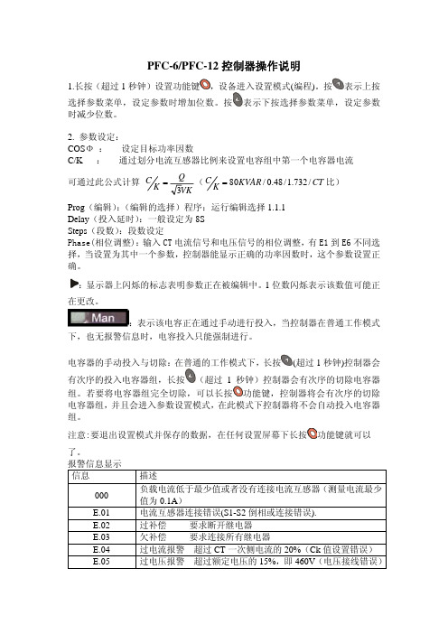
PFC-6/PFC-12控制器操作说明1.长按(超过1秒钟)设置功能键,设备进入设置模式(编程)。
按表示上按选择参数菜单,设定参数时增加位数。
按表示下按选择参数菜单,设定参数时减少位数。
2. 参数设定:COS Φ : 设定目标功率因数C/K : 通过划分电流互感器比例来设置电容组中第一个电容器电流 可通过此公式计算 VK QK C 3=(CT KVAR K C /732.1/48.0/80=比)Prog (编辑):(编辑的选择)程序:运行编辑选择1.1.1Delay (投入延时):一般设定为8SSteps (段数):段数设定Phase(相位调整):输入CT 电流信号和电压信号的相位调整,有E1到E6不同选择,当设置为其中一个参数,控制器能显示正确的功率因数时,这个参数设置正确。
:显示器上闪烁的标志表明参数正在被编辑中。
1位数闪烁表示该数值可能正在更改。
:表示该电容正在通过手动进行投入,当控制器在普通工作模式下,也无报警信息时,电容投入只能强制进行。
电容器的手动投入与切除:在普通的工作模式下,长按(超过1秒钟)控制器会有次序的投入电容器组,长按(超过1秒钟)控制器会有次序的切除电容器组。
若要将电容器组完全切除,可以长按功能键,控制器将会有次序的切除电容器组,并且会进入参数设置模式,在此模式下控制器将不会自动投入电容器组。
注意:要退出设置模式并保存的数据,在任何设置屏幕下长按功能键就可以了。
报警信息显示信息描述 000负载电流低于最少值或者没有连接电流互感器(测量电流最少值为0.1A ) E.01电流互感器连接错误(S1-S2倒相或连接错误). E.02过补偿 要求断开继电器 E.03欠补偿 要求连接所有继电器 E.04过电流报警 超过CT 一次侧电流的20%(Ck 值设置错误) E.05过电压报警 超过额定电压的15%,即460V (电压接线错误)。
- 1、下载文档前请自行甄别文档内容的完整性,平台不提供额外的编辑、内容补充、找答案等附加服务。
- 2、"仅部分预览"的文档,不可在线预览部分如存在完整性等问题,可反馈申请退款(可完整预览的文档不适用该条件!)。
- 3、如文档侵犯您的权益,请联系客服反馈,我们会尽快为您处理(人工客服工作时间:9:00-18:30)。
PFC控制器操作说明
PFC(功率因数校正)控制器是一种用来提高电路功率因数的装置,
主要用于改善交流电路的负载电流波形,实现功率因数的校正,从而提高
系统的能效。
在实际应用中,PFC控制器通过改变输出电流和电压的相位
关系,将负载电流和电压进行匹配,使得负载电流呈现正弦波形,并且与
电压保持同相位,从而减少电路中谐波电流的产生,提高电路的功率因数。
下面是PFC控制器的操作说明:
1.接线连接:将PFC控制器的输入端与电源连接,通过接线端子将交
流电源的线缆连接到PFC输入端;将PFC控制器的输出端与负载设备连接,通过接线端子将负载设备的线缆连接到PFC输出端。
2.调节工作模式:PFC控制器通常具有两种工作模式,即恒定电流模
式和恒定电压模式。
根据实际需要,选择合适的工作模式。
如果负载设备
需要恒定电流供应,则选择恒定电流模式;如果负载设备需要恒定电压供应,则选择恒定电压模式。
3.设置参数:根据负载设备的需求,设置合适的参数。
PFC控制器通
常具有参数调节功能,如输出电流、输出电压、频率等参数可以通过旋钮
或按键进行调节。
根据负载设备的额定值,逐步调节这些参数,以获得理
想的工作状态。
4.监测工作状态:通过PFC控制器上的显示屏或指示灯,可以实时监
测设备的工作状态。
显示屏上通常会显示当前的工作模式、参数数值等信息,指示灯也会显示设备的运行状态。
根据这些信息,可以及时发现并解
决设备故障或异常。
5.定期维护保养:为了保持PFC控制器的正常工作状态,需要定期对
其进行维护保养。
首先,需要对控制器进行清洁,以防止灰尘或污垢进入
设备导致故障。
其次,需要检查控制器的连接线路是否松动,若有松动现
象需要重新固定。
另外,还需要检查控制器的散热情况,如果散热不良可
能会导致过热现象,需要及时解决。
6.故障排除:当PFC控制器出现故障时,需要进行相关的故障排除。
首先,检查设备的电源是否正常,可能是由于电源故障导致控制器无法正
常工作。
其次,检查设备的电路是否连接正确,可能是由于接线不良导致
控制器无法与负载正常通信。
最后,根据故障提示信息进行相关的故障处理,可能需要替换故障组件或进行维修。
以上就是PFC控制器的操作说明,通过正确的接线连接、调节工作模式、设置参数、监测工作状态、定期维护保养和故障排除,可以确保PFC
控制器的正常运行,提高系统的能效。
在操作过程中,需要注意安全规范,避免电击、短路和火灾等安全事故的发生。