黑磷与石墨烯的文献
下一个市场爆发点:堪比石墨烯的“梦幻材料”黑磷

下一个市场爆发点:堪比石墨烯的“梦幻材料”黑磷
北极星输配电网讯:【摘要】作为刚刚兴起两三年的新材料,石墨烯行业尚处于资本和产业群雄逐鹿时代。
然而,另一种新型单元素二维原子晶体材料黑磷被发现,与石墨烯类似,黑磷具有诸多优异特性,故被称为比肩石墨烯的梦幻材料。
黑磷的研究和应用才刚开始,其非线性光学特性被国内外多家单位证实并应用于超快激光的产生中。
可以预见不久的将来,它将成为第二个石墨烯。
首先,我们来了解一下石墨烯和黑磷究竟是什么东西?
石墨烯(二维碳材料)
手机充电只需几秒钟?史上最薄电灯泡?光驱动飞行器?关于石墨烯非凡应用的新闻不断出现在人们的视野当中,似乎石墨烯已经成为了无所不能的超级材料。
石墨烯是什么?
石墨烯(Graphene)是从石墨材料中剥离出来、由碳原子组成的只有一层原子厚度的二维晶体。
2004 年,英国曼彻斯特大学物理学家安德烈˙盖姆和康斯坦丁˙诺沃肖洛夫,成功从石墨中分离出石墨烯,证实它可以单独存在,两人也因此共同获得2010 年诺贝尔物理学奖。
石墨烯既是最薄的材料,也是最强韧的材料,断裂强度比最好的钢材还要高200 倍。
同时它又有很好的弹性,拉伸幅度能达到自身尺寸的20%。
它是目前自然界最薄、强度最高的材料,假如用一块面积1 平方米的石墨烯做成吊床,本身重量不足1 毫克便可以承受一只一千克的猫。
石墨烯目前最有潜力的应用是成为硅的替代品,制造超微型晶体管,用来生产未来的超级计算机。
用石墨烯取代硅,计算机处理器的运行速度将会快数百倍。
二维纳米材料黑磷的光电特性研究进展

范德 华 力作用 【7】。黑磷 独特 的褶皱结 构,使它 展现 出 性 ,在生物 医学领 域具 有其他 无机 纳米材 料不 具备 的
有别 于 其他 二维材 料 的优 异性 质和应 用 。首先 ,与 石 天 然 优 势 。 本 文 主 要 介 绍 了 黑 磷 的 几 种 制 备 方 法 , 并
第 38卷 第 4期 2018年 08月
物 理 学 进 展
PROG RESS IN PHYSICS
Vo1.38 N O.4 A ug. 2018
二维 纳 米 材 料 黑磷 的光 电特 性研 究进 展
尤 凯熹,范涛健 ,葛颜绮 ,张 晗
深 圳大学黑磷 光电I程实验 室,光电协同刨新中心,光 电I程学院
关键 词:二维材料;黑磷制备;光电特性;光电应用
中图分类号 : 0799 文献标 识码 : A
DOI:10.13725/j.cnki.pip.2018.04.002
3
M 4 4 5 5 6
6 6 7 7
" " " " " " 8 8 8 O 0 O l l
文章编号:1000—0542(2018)04—0163—12
163
164
(a)
尤凯熹等:二维纳 米材料 黑磷的光电特 性研究进展
(c)
团
(b)
C
b
b
a
C
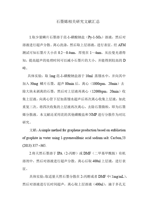
图 1.(a)和 (b)在 ac和 平面 t的 单层 BP 的投影 。上 部和下部原子 分别 以浅色和深色 呈现 。(C)品胞 的示意图 .  ̄_1 /-J 卡啊 邻层之间的 1ቤተ መጻሕፍቲ ባይዱ2单位的偏移 [71
分 稳 定 。层 内 具 有 较 强 的 共 价 键 , 并 还 留 有 个 的 电 胞 中 , 一 个 成 人 体 内就 含 有 600 ̄900 g 的磷 , I 人 体
有关石墨烯的文献

石墨烯作为一种由单层碳原子组成的二维材料,自发现以来就引起了广泛的研究兴趣。
它在许多领域,如电子学、能源和材料科学,都展示了其独特的性质和潜在的应用。
以下是几篇关于石墨烯的重要文献,具体内容可能涉及石墨烯的结构、性质和应用等方面的研究。
1. 王中林团队在《科学》杂志上发表的关于石墨烯的论文,对石墨烯的性质和应用进行了深入的探讨。
文中详细阐述了石墨烯的电子结构、力学性质以及在电子器件和能源领域的应用。
同时,也讨论了石墨烯制备的新方法及其工业化可能面临的挑战。
2. 另一篇重要的文献是来自曼彻斯特大学的关于石墨烯场效应管的论文。
该论文详细研究了石墨烯中的电荷转移和电子输运行为,这些研究对于理解石墨烯的物理性质和开发新的石墨烯器件至关重要。
3. 赵东保团队的论文详细研究了石墨烯的化学稳定性。
这篇文章讨论了石墨烯在各种化学环境中的稳定性,这对于石墨烯的实际应用和长期稳定性至关重要。
4. 还有一篇文献对石墨烯的制备技术进行了深入探讨,包括化学气相沉积、机械剥离、以及在溶液中的制备方法等。
文章分析了各种制备方法的优缺点,并讨论了如何进一步提高石墨烯的质量和产量。
5. 最后,一篇综述文章汇总了近年来石墨烯在各个领域的研究进展,包括电子学、光学、磁学、生物医学等。
这篇文章为读者提供了石墨烯研究的全面概述,有助于了解石墨烯在不同领域的应用前景。
以上文献均对石墨烯的性质、结构和应用进行了深入的研究和探讨,但具体的内容可能会因研究角度和数据更新而有所不同。
此外,石墨烯的研究是一个持续发展的领域,新的研究成果和方法也层出不穷,因此阅读最新的研究文献是获取最前沿信息的关键。
基于石墨烯和黑磷的太赫兹窄带吸收结构。

基于石墨烯和黑磷的太赫兹窄带吸收结构。
下载提示:该文档是本店铺精心编制而成的,希望大家下载后,能够帮助大家解决实际问题。
文档下载后可定制修改,请根据实际需要进行调整和使用,谢谢!本店铺为大家提供各种类型的实用资料,如教育随笔、日记赏析、句子摘抄、古诗大全、经典美文、话题作文、工作总结、词语解析、文案摘录、其他资料等等,想了解不同资料格式和写法,敬请关注!Download tips: This document is carefully compiled by this editor. I hope that after you download it, it can help you solve practical problems. The document can be customized and modified after downloading, please adjust and use it according to actual needs, thank you! In addition, this shop provides you with various types of practical materials, such as educational essays, diary appreciation, sentence excerpts, ancient poems, classic articles, topic composition, work summary, word parsing, copy excerpts, other materials and so on, want to know different data formats and writing methods, please pay attention!基于石墨烯和黑磷的太赫兹窄带吸收结构1. 引言在电磁波频谱中,太赫兹波段(0.1至10太赫兹)因其在生物医学、安全检测和通信等领域的潜在应用而备受关注。
关于石墨烯的参考文献

关于石墨烯的参考文献石墨烯是由未来材料学大师安德烈·海姆(Andre Geim)和康斯坦丁·诺沃肖洛夫(Konstantin Novoselov)于2004年发现的一种新型碳材料。
这种材料的发现颠覆了传统碳材料的应用前景和开拓领域。
以下是对石墨烯的参考文献的内容生动、全面、有指导意义的分析和总结。
1. 《石墨烯基纳米复合材料在生物医学领域的应用研究综述》本文详细分析了石墨烯基纳米复合材料在生物医学领域的应用。
石墨烯因其出色的导电性、导热性和高强度,被广泛地应用于生物医学领域。
将石墨烯与纳米材料复合可以改善石墨烯的可溶性和生物相容性,扩展了其应用范围。
这篇文章通过实例和案例详细阐述了石墨烯基纳米复合材料在生物医学领域中的特点和应用。
2. 《石墨烯光电器件的研究进展与展望》本文介绍了石墨烯光电器件在研究方面的进展和展望。
石墨烯具有极高的光电转换效率和广泛的吸收光谱范围,这使得它在制作光电器件方面具有天生优势。
在这篇文章中,作者以石墨烯光电器件的制备和性能控制为切入点,通过回顾石墨烯光电器件的研究进展,提出了一些可能的研究方向和未来发展趋势。
3. 《石墨烯复合材料填充剂的制备及其应用研究》本文主要研究石墨烯复合材料填充剂的制备及其应用研究。
石墨烯的出色性能和纳米级别的粒度,使其成为一种理想的高效填充剂。
在石墨烯掺杂的材料中,它能够显著提高材料的强度、硬度和热导率等性能。
这篇文章通过实验研究探索了石墨烯复合材料填充剂的制备方法和应用场景,并提出了具体的操作规范和注意事项。
4. 《石墨烯电池的制备与应用研究》本文重点研究了石墨烯电池的制备和应用。
石墨烯因其出色的导电性和机械性能,成为电池制备领域不可或缺的材料。
在石墨烯电池的制备和应用方面,本文详细介绍了纳米和复合石墨烯电极的制备方法、应用场景和性能等方面的特点。
基于实验结果,文章提出了石墨烯电池应用的展望和未来可能的研究方向。
总之,石墨烯是一种未来具有巨大潜力的材料。
石墨烯相关研究文献汇总
石墨烯相关研究文献汇总1.取少量鳞片石墨溶于芘-1-磺酸钠盐(Py-1-SO3)溶液,然后对溶液进行超声分散、离心洗涤,然后取上层溶液,进行表征。
经AFM 测试可知石墨片大小在0.2~0.4um,厚度在1~4nm。
从拉曼光谱得知,提高超声的处理时间可以减小石墨片的大小,并能得到较高的D 峰。
具体实验:取1mg芘-1-磺酸钠盐溶于10ml 蒸馏水中,并向其中加入30mg 鳞片石墨,超声80min后,离心(1000rpm,20min)去除大块未剥离的石墨,然后对上层液再离心(12000rpm,20min)收集上层液,向离心管下层加蒸馏水超声后再次离心收集上层液,如此重复三次。
将四次收集的上层液再次离心,去除石墨微粒,即为石墨烯分散液。
本文献还采用芘的其他磺酸盐和NMP进行分散作为对比研究。
文献:A simple method for graphene production based on exfoliation of graphite in water using 1-pyrenesulfonic acid sodium salt. Carbon,53 (2013) 357 –365.2.将天然石墨溶于IPA(2-丙醇)或DMF(二甲基甲酰胺)有机溶剂中,然后对溶液进行超声分散、离心后取400ul上层液,进行表征。
具体实验:取适量天然石墨分散在2-丙醇或者DMF中(1mg/mL),然后对溶液进行长时间超声,离心取上层溶液(400ul),滴于多孔无定形碳上(400目)进行TEM测试,另取400ul滴于氧化硅基底或者玻璃基底上,进行SEM及拉曼测试。
本文对不同的超声时间、有机溶剂以及超声时水的温度做了系统的探究,得出以下结论:随着超声时间的增加,石墨的碎片化显著增加(通过拉曼光谱ID /IG=C(λ)/La,La石墨碎片的平均尺寸);石墨分散在一些与其表面自由能相近的溶剂中,其混合后的晗变接近于零,这样剥离石墨烯所需的能量较小(这样溶剂-石墨的相互作用是范德华力而不是共价键)。
新型二维晶体材料——磷烯综述——博士生《材料科学与工程选论》

北京科技大学材料科学与工程学院博士生《材料科学与工程选论》学习报告报告题目:新型二维晶体材料——黑磷烯学号:作者:越迷贝贝导师:专业名称:材料科学与工程2016年5月8日北京科技大学材料科学与工程学院博士研究生《材料科学与工程选论》课程报告目录摘要 (I)Abstract (II)1 引言 (1)2 二维晶体材料的发展 (2)2.1二维晶体材料的发展背景 (2)2.2二维晶体材料的优越性 (4)3 黑磷烯的性能 (6)3.1 黑磷烯的晶格结构 (6)3.2黑磷烯的表征 (7)3.3 黑磷烯的带隙 (8)3.4 黑磷烯的各向异性 (11)3.5 黑磷烯的光子学特性 (13)4 黑磷烯的制备 (15)4.1 机械剥离法 (15)4.2 液相剥离法 (17)4.3 化学合成法 (19)5 黑磷烯的应用 (21)5.1 场效应晶体管 (21)5.2 其他应用 (24)6 发展与展望 (27)参考文献 (29)摘要随着信息技术的不断发展,传统三维半导体材料即将到达瓶颈。
而新型二维晶体材料——黑磷烯很有希望替代传统半导体材料。
作为刚发现的一种二维晶体材料,黑磷烯的研究仍然处于起步阶段。
本文综述了黑磷烯拥有的独特性能,现有的制备方法及可能的应用领域等。
黑磷烯具有褶皱蜂窝状结构,其二维晶体结构类似石墨烯,非常稳定。
黑磷烯具有直接带隙,且其带隙能随着黑磷烯的层数改变而在0.3eV-2eV之间改变。
因为其独特的晶体结构,黑磷烯在光学、电学及力学方面都有不同于其他二维晶体的各向异性。
黑磷烯的制备目前主要有3种方法,包括机械剥离法、液相剥离法和化学合成法。
由于黑磷烯优异的各项性能,使得它在场效应晶体管及光电设备等方面都有非常广阔的发展前景。
但是,黑磷烯的大规模应用目前来看还需努力。
因为黑磷烯存在两大问题:其一,在空气中非常不稳定,容易老化;其二,目前的制备方法仍然无法大规模低成本地制备出可供工业应用的黑磷烯。
关键字:二维晶体材料,黑磷烯,半导体,性能,制备Black Phosphorene,a New Kind of 2-D Crystal MaterialAbstractAs the development of information technology, the development of traditional 3-D materials will reach the bottlenecks before long. The new kind of 2-D crystal material, black phosphorene, is regarded as an alternative to the traditional 3-D materials. Black phosphorene was discovered in the recent years, and the research of black phosphorene is still in its infancy. This paper reviews the unique properties, the preparation methods and the possible application areas of black phosphorene. Black phosphorene has a direct band-gap, which ranges from 0.3eV to 2eV as the layer changes. Because of the special crystal structure, black phosphorene displays anisotropic in optical, mechanical and electrical properties. Heretofore, there are 3 kinds of preparation methods of black phosphorene, including mechanical exfoliation, liquid exfoliation and chemical synthesis. It is acknowledged that black phosphorene can play a big role in the field of field effect transistor(FET) and photoelectric equipment because of its excellent performances. However, many works remain to be done for the practical application of black phosphorene. More attention should be paid to two problems: firstly, black phosphorene is not stable in the air and it is easy to aging; secondly, black phosphorene is difficult to put into mass production by current reparation methods.Key words: 2-D crystal material, Black phosphorene, Semiconductor, Property, Preparation1 引言从石器时代到青铜时代、铁器时代,再到现代的信息时代,人类社会文明的发展史从某个意义上来说也是一部材料的进化史。
黑磷的制备及储能应用研究进展
Vol.53 No.6June,2021第53卷第6期2021 年 6 月无机盐工业INORGANIC CHEMICALS INDUSTRYDoi:10.19964/j.issn.1006-4990.2021-0245开放科学(资源服务)标志识码(OSID )黑磷的制备及储能应用研究进展蒋运才1 袁2袁3袁4袁李雪梅 r 吴兆贤 r 曹昌蝶1袁梅 毅心,廉培超1袁2袁3(1.昆明理工大学化学工程学院,云南昆明650500;2.云南省磷化工节能与新材料重点实验室;3.云南省高校磷化工重点实验室;4.昆明黑磷科技服务有限责任公司)摘 要:黑磷作为一种新型的精细磷化工产品,因其高的理论比容量、高的载流子迁移率及良好的导电性而在储能 领域具有很好的应用前景。
近年来,针对黑磷、纳米黑磷的制备及其储能应用,涌现岀了许多新技术、新方法与新策略。
在黑磷的制备方面,开发了加压法(高压法、机械球磨法)和催化法(祕熔化法、汞回流法、矿化法)制备技术,但仍未能实现 黑磷的连续化制备;在纳米黑磷的制备方面,开发了自上而下法(机械剥离法、超声剥离法、剪切剥离法、电化学剥离法)和 自下而上法(溶剂热法、化学气相沉积法),然而,高质量、高产率纳米黑磷的精确可控制备技术还有待开发。
此外,黑磷在应用于储能领域时,大的体积膨胀使得电池储能性能变差,通过纳米化并与其他材料复合制备纳米黑磷基复合材料,发挥协同作用,一定程度上能够缓解以上问题。
从黑磷、纳米黑磷的制备及其在储能领域的应用三个方面进行综述,旨在为 高品质黑磷及纳米黑磷的高效率、低成本、可控及规模化制备提供借鉴思路,为其在储能领域的发展方向奠定基础。
关键词:黑磷;纳米黑磷;制备技术;纳米黑磷基复合材料;储能中图分类号:TQ126.31 文献标识码:A 文章编号:1006-4990(2021)06-0059-13Research progress on preparation and application in energy storage of black phosphorusJiang Yuncai 1,2,3,4,Li Xuemei 1,2,3,4, Wu Zhaoxian 1,2,3,4,Cao Changdie 1 袁 Mei Yi 1,2,3, Lian Peichao 1,2,3(1.Faculty of Chemical Engineering , Kunming University of S cience and Technology , Kunming 650500, China ;2.Yunnan Province Key Laboratory of E nergy Saving in Phosphorus Chemical Engineering and New Phosphorus Materials ;3.The Higher Educ r ational Key Laboratory f or Phosphorus Chemical Engineering of Y u nnan Province ;4.Kunming Black Phosphorus Technology Service Limited Company)Abstract : As a novel fine phosphorus chemical product , black phosphorus has a promising application prospect in energy ator-age due to its high theoretical specific capacity , high carrier mobility, and good conductivity.In recent years , many new techno logies , methods , and strategies have been emerged for the preparation and energy storage application of black phosphorus and nano-black phosphorus.In terms of the preparation of black phosphorus , the prepared techniques of pressurized method (highpressure method ,mechanical ball milling method ) and catalytic method (bismuth melting method ,mercury reflux method and mineralization method ) have been developed.However, the continuous preparation of black phosphorus was still not realized ; in the aspect of the preparation of nano-black phosphorus , the top-down method (mechanical stripping , ultrasonic stripping ,shear stripping , electrochemical stripping ) and bottom-up method ( solvothermal method , chemical vapor deposition method )have been developed.Nevertheless ,the precise controllable preparation technology of high-quality and high-yield nano-black phosphorus has yet to be developedAdditionally ,when black phosphorus is applied in energy storage , the occurrence of large volumeexpansion would lead to poor energy storage performance of t he battery.The nano-black phosphorus matrix composites are prepared by nanosizing and compounding with other materials to play a synergistic role , which can alleviate the above problem to a certainextent.The three aspects including the preparation black phosphorus and nano-black phosphorus , and its application in energy storage were reviewed , aiming to provide a reference idea for efficient , low-cost , controllable and largescale preparation ofblack phosphorus and nano-black phosphorus, and lay the foundation for its development direction in the field of energy storage. Key words : black phosphorus ; nano black phosphorus ; preparation techniques ; nano black phosphorus matrix composite ma-terials ; energy storage随着世界各国经济的繁荣发展,全球对能源的 需求量与日俱增,大量使用化石能源所带来环境污染的问题逐渐凸显。
- 1、下载文档前请自行甄别文档内容的完整性,平台不提供额外的编辑、内容补充、找答案等附加服务。
- 2、"仅部分预览"的文档,不可在线预览部分如存在完整性等问题,可反馈申请退款(可完整预览的文档不适用该条件!)。
- 3、如文档侵犯您的权益,请联系客服反馈,我们会尽快为您处理(人工客服工作时间:9:00-18:30)。
Electronic Structures of Hybrid Graphene/Phosphorene NanocompositeWei Hu,1,2,∗Tian Wang,3and Jinlong Yang 2,4,†1Computational Research Division,Lawrence Berkeley National Laboratory,Berkeley,CA 94720,USA2Hefei National Laboratory for Physical Sciences at Microscale,University of Science and Technology of China,Hefei,Anhui 230026,China3Department of Precision Machinery and Precision Instrumentation,University of Science andTechnology of China,Hefei,Anhui 230026,China 4Synergetic Innovation Center of Quantum Information and Quantum Physics,University of Science and Technology of China,Hefei,Anhui 230026,China(Dated:November 10,2014)Combining the electronic structures of two-dimensional monolayers in ultrathin hybrid nanocom-posites is expected to display new properties beyond their simplex components.Here,first-principles calculations are performed to study the structural,electronic and optical properties of hybrid graphene and phosphorene nanocomposite.It turns out that weak van der Waals interactions dominate between graphene and phosphorene with their intrinsic electronic properties preserved.Hybrid graphene and phosphorene nanocomposite shows tunable band gaps at graphene’s Dirac point and a transition from hole doing to electron doing for graphene as the interfacial distance decreases.Charge transfer between graphene to phosphorene induces interfacial electron-hole pairs in hybrid graphene and phosphorene nanocomposite with enhanced visible light response.I.INTRODUCTIONTwo-dimensional (2D)ultrathin materials,such as graphene,[1,2]silicene,[3,4]hexagonal boron nitride,[5,6]graphitic carbon nitride,[7,8]graphitic zinc oxide,[9,10]molybdenum disulphide,[11,12]have received consid-erable interest recently owing to their outstanding prop-erties and potential applications.Graphene,[2]a 2D sp 2-hybridized carbon monolayer,is known to have remark-able electronic properties,such as a high carrier mobil-ity,but the absence of a bandgap limits its applications of large-offcurrent and high on-offratio for graphene-based electronic devices.Furthermore,intrinsic elec-tronic properties of graphene depend sensitively on the substrates due to strong graphene-substrate interactions,such as SiO 2,[13,14]SiC[15,16]and metal[17,18]sur-faces.Therefore,opening a small bandgap and finding an ideal substrate for graphene remains challenging in the experiments.2)[31–33]nanocomposites show much more new properties far beyond their simplex components.Furthermore,most of them are ideal substrates for graphene to preserve the intrinsic electronic properties of graphene and substrates.∗Corresponding author.E-mail:whu@†Correspondingauthor.E-mail:jlyang@Most recently,a new 2D material,namely,black phosphorus monolayer or phosphorene,[34–37]has been isolated in the experiments through mechanical exfo-liation from bulk black phosphorus and has immedi-ately received considerable attention.Phosphorene also shows some remarkable electronic properties superior to graphene.For example,phosphorene is a semiconductor with a direct bandgap of about 1eV ,[35]showing the drain current modulation up to 105and carrier mobil-ity up to 103cm 2/(Vs)in nanoelectronics.[36]Here,an interesting question arise:whether graphene and phos-phorene can form a 2D hybrid G/P nanocomposite with new properties?In the present work,we design a new 2D hybrid graphene and phosphorene nanocomposite and study its electronic and optical properties with first-principles calculations.The results show that graphene inter-acts overall weakly with phosphorene via van der Waals (vdW)interactions,thus,their intrinsic electronic prop-erties can be preserved in hybrid graphene/phosphorene nanocomposite.Moreover,interlayer interactions in hy-brid graphene/phosphorene nanocomposite can induce tunable band gaps at graphene’s Dirac point,a transi-tion from hole doing to electron doing for graphene and enhanced visible light response.II.THEORETICAL METHODS AND MODELSThe lattice parameters of graphene and phosphorene calculated to setup unit cell are a (G)=b (G)=2.47˚A ,[19]a (P)=4.62˚A and b (P)=3.30˚A .[35]We design a new 2D hybrid graphene/phosphorene nanocomposite (40carbon atoms and 28phosphorus atoms)as shown in Figure 1with a small lattice mismatch less than 2%.The vacuum space in the Z direction is about 15˚A to separate the interactions between neighboring slabs.a r X i v :1411.1781v 1 [c o n d -m a t .m t r l -s c i ] 6 N o v 2014FIG.1:(Color online)Geometric structures of hybrid graphene/phosphorene nanocomposite ((a)top and (b)side views).The gray and violet balls denote carbon and phos-phorus atoms,respectively.First-principles calculations are based on the den-sity functional theory (DFT)implemented in the VASPpackage.[38]The generalized gradient approximation of Perdew,Burke,and Ernzerhof (GGA-PBE)[39]with van der Waals (vdW)correction proposed by Grimme (DFT-D2)[40]is chosen due to its good description of long-range vdW interactions.[41–49]As an benchmark,DFT-D2calculations give a good bilayer distance of c =3.25˚A and binding energy of E b =-25meV per carbon atom for bilayer graphene,which fully agree with previous experimental[50,51]and theoretical[52,53]studies.The energy cutoffis set to be 500eV .The surface Brillouin zone is sampled with a 3×3regular mesh and 120k points are used for calculating the tiny band gaps at the Dirac point graphene in the hybrid G/P nanocomposite supercell.All the geometry structures are fully relaxed until energy and forces are converged to 10−5eV and 0.01eV /˚A ,respectively.To investigate the optical properties of hybrid G/P nanocomposite,the frequency-dependent dielectric ma-trix is calculated.[54]In order to calculate the optical properties of hybrid G/P nanocomposite,a large 6×6regular mesh for the surface Brillouin zone,a large num-ber of empty conduction band states (two times more than the number of valence band)and frequency grid points (2000)are adopted.We crosscheck the optical properties of graphene and phosphorene,consistent with previous theoretical calculations.[19,37]III.RESULTS AND DISCUSSIONElectronic properties of pristine graphene and phos-phorene monolayers in the supercells are checked first and their electronic band structures are plotted in Figure 2aand 2b.Graphene is a zero-gap semiconductor (Figure 2a),showing a linear Dirac-like dispersion relation E (k )=± νF |k |around the Fermi level where νF is the Fermi velocity,and νF (G )=0.8×10⁶m/s at the Dirac point of graphene.Monolayer phosphorene is semiconducting with a direct band gap of 0.85eV (Figure 2b),which agrees well with previous theoretical studies.[35]FIG.2:(Color online)Electronic band structures of (a)graphene,(b)phosphorene and (c)hybrid graphene/phosphorene nanocomposite.The Fermi level is set to zero and marked by green dotted lines.We then study the geometric structures of hybrid G/P nanocomposite.Typical vdW equilibrium spacing of about 3.43˚A with corresponding small binding energy of about -24.7meV per atom of graphene is obtained for hybrid G/P nanocomposite,which is well comparable with recent theoretical calculations in 2D graphene based nanocomposites,such as G/S,[19]G/g-BN,[24]G/g-C 3N 4,[27]G/g-ZnO[28]and G/MoS 2.[31]Thus,weak vdW interactions dominate between graphene and phos-phorene,suggesting that phosphorene can be used as an ideal substrate for graphene with their intrinsic electronic structures undisturbed.Notice that the small lattice mis-match of about 2%for graphene and phosphorene has little effect on their electronic properties in hybrid G/P nanocomposite.Electronic band structure of hybrid G/P nanocompos-ite is shown in Figure 2c.The Dirac point of graphene is still preserved,and the Fermi velocity at the Dirac point is almost unchanged (νF (G/P )=0.8×10⁶m/s )in hybrid G/P nanocomposite compared to free-standing graphene,though small band gap of 10meV is opened at the Dirac point of grpahene.Notice that induced band gaps at the Dirac point of graphene are typically sen-sitive and tunable to other external conditions,such as interlayer separation,[19]as plotted in Figure 3.The gap values at graphene’s Dirac point increase from 5to 90meV as the interfacial distance decreases from 3.7to 2.7˚A in hybrid G/P nanocomposite,showing a potential for high-performance graphene-based electronicdevices.FIG.3:(Color online)The band gap opened at graphene’s Dirac point in hybrid graphene/phosphorene nanocomposite as a function of interfacial distance.Interestingly,we find that the Dirac point of graphene moves form the conduction band to the valence band of phosphorene as the interfacial distance decreases from 4.5to 2.7˚A in hybrid G/P nanocomposite,inducing a transition from hole (p-type)doping to electron (n-type)doping for graphene as shown in Figure 4.When the interfacial distance artificially increases larger than 4.5˚A ,graphene’s Dirac point is close to phosphorene’s con-duction band.That is because graphene’s work function (4.3eV )is close to phosphorene’s nucleophilic potential (4.1eV ).Based on the Schottky-Mottmodel,[55]elec-trons easily transfer from graphene to phosphorene,re-sulting in p-type doping of graphene.But,weak over-lap of electronic states between graphene and phos-phorene are enhanced as the interfacial distance de-creases.Furthermore,carbon has a large electroneg-ativity (2.55)than that (2.19)of phosphorus.Thus,when graphene and phosphorene are close to each other (smaller than 3.0˚A ),electrons easily transferred from phosphorene to graphene,resulting in n-type doping of graphene.Similarly,interlayer-interaction induced a transition from p-type doping to n-type doping for graphene has also observed experimentally and theoreti-cally in hybrid graphene/silicene nanocomposite[19]and graphene adsorption on some metal substrates.[17]Besides commonly focused electronic structures in 2D graphene based nanocomposites,we also study the opti-cal properties in hybrid G/P nanocomposite.Though pristine graphene and phosphorene themselves display unique optical properties,[19,37]interlayer interactions and charge transfer in 2D nanocomposites may induce new optical transitions.[8,28]As shown in Figure 5,charge transfer between graphene to phosphorene inducesFIG.4:(Color online)Electronic band structures of hybrid graphene/phosphorene nanocomposite at different interfacial distances D =2.8,3.0,3.5,4.0and 4.5˚A .The Fermi level is set to zero and marked by green dotted lines.interfacial electron-hole pairs in hybrid G/P nanocom-posite.In optical property calculations,the imaginary part of dielectric function for graphene and phospho-rene monolayers as well as corresponding hybrid G/P nanocomposite are evaluated,including the light polar-ized parallel and perpendicular to the plane,as shown in Figure 5.Parallel optical absorption of pristine graphene and phosphorene monolayers mainly possesses in the vis-ible light range from 200to 1000nm due to the tran-sitions from πto π∗states and σto σ∗states.Hybrid G/P nanocomposite exhibits stronger optical absorption,especially in the visible light range from 300to 800nm ,compared with simplex graphene and phosphorene mono-layers,because the interlayer coupling in hybrid G/P nanocomposite induces electronic states overlap and elec-trons can now be directly excited between graphene and phosphorene.But,perpendicular dielectric function is al-most unaffected by the interlayer interactions in hybrid G/P nanocomposite due to very weak optical absorption of graphene in this direction.IV.CONCLUSIONSIn summary,we study the electronic structures and optical properties of hybrid graphene/phosphorene nanocomposite with first-principles calculations.We find that phosphorene interacts weakly with graphene via weak vdW interactions to preserve their intrin-sic electronic properties.Moreover,interlayer interac-tions can induce tunable band gaps at graphene’s Dirac point,a transition from hole doing to electron doing for graphene and enhanced visible light response in hy-brid graphene/phosphorene nanocomposite.With theFIG.5:(Color online)Imaginary part of frequency depen-dent dielectric function((a)parallel and(b)perpendicular) for pristine graphene and phosphorene monolayers as well as corresponding hybrid graphene/phosphorene nanocom-posite.Differential charge density(0.002e/˚A3)of hybrid graphene/phosphorene nanocomposite is shown in the insert.excellent electronic and optical properties combined be-yond simplex graphene and phosphorene monolayers,2D ultrathin hybrid graphene/phosphorene nanocomposite system is expected to be of a great potential in new graphene-based electronic devices.V.ACKNOWLEDGMENTSThis work is partially supported by the National Key Basic Research Program(2011CB921404),by NSFC (11404109,21121003,91021004,21233007,21222304), by CAS(XDB01020300).This work is also partially supported by the Scientific Discovery through Advanced Computing(SciDAC)program funded by U.S.Depart-ment of Energy,Office of Science,Advanced Scientific Computing Research and Basic Energy Sciences(W.H.). We thank the National Energy Research Scientific Com-puting(NERSC)center,USTCSCC,SC-CAS,Tianjin, and Shanghai Supercomputer Centers for the computa-tional resources.[1]K.S.Novoselov,A.K.Geim,S.V.Morozov,D.Jiang,Y.Zhang,S.V.Dubonos,I.V.Grigorieva,and A.A.Firsov,Scinece306,666(2004).[2]A.K.Geim and K.S.Novoselov,Nature Mater.6,183(2007).[3]S.Cahangirov,M.Topsakal,E.Akt¨u rk,H.S¸ahin,and S.Ciraci,Phys.Rev.Lett.102,236804(2009).[4]A.Kara,H.Enriquez, A.P.Seitsonend,L. C.L.Y.Voone,S.Vizzini,B.Aufrayg,and H.Oughaddoub,Surf.Sci.Rep.67,1(2012).[5]K.Watanabe,T.Taniguchi and H.Kanda,Nature Mater.3,404(2004).[6]L.Song,L.Ci,H.Lu,P.B.Sorokin,C.Jin,J.Ni,A.G.Kvashnin,D.G.Kvashnin,J.Lou,B.I.Yakobson and P.M.Ajayan,Nano Lett.10,3209(2010).[7]X.Wang,K.Maeda,A.Thomas,K.Takanabe,G.Xin,J.M.Carlsson,K.Domen and M.Antonietti,Nature Mater.8,76(2009).[8]F.Wu,Y.Liu,G.Yu,D.Shen,Y.Wang,and E.Kan,J.Phys.Chem.Lett.3,3330(2012).[9]F.Claeyssens,C.L.Freeman,N.L.Allan,Y.Sun,M.N.R.Ashfold,and J.H.Harding,J.Mater.Chem.15, 139(2005).[10]C.L.Freeman,F.Claeyssens,and N.L.Allan,Phys.Rev.Lett.96,066102(2006).[11]K.F.Mak,C.Lee,J.Hone,J.Shan,and T.F.Heinz,Phys.Rev.Lett.105,136805(2010).[12]B.Radisavljevic,A.Radenovic,J.Brivio,V.Giacometti,and A.Kis,Nature Nanotech.6,147(2011).[13]J.Martin,N.Akerman,G.Ulbricht,T.Lohmann,J.H.Smet,K.von Klitzing,and A.Yacoby,Nature Phys.4, 144(2008).[14]N.T.Cuong,M.Otani,and S.Okada,Phys.Rev.Lett.106,106801(2011).[15]S.Y.Zhou,G.-H.Gweon,A.V.Fedorov,P.N.First,W.A.de Heer,D.-H.Lee,F.Guinea,o,and A.Lanzara,Nature Mater.6,770(2007).[16]J.Ristein,S.Mammadov,and T.Seyller,Phys.Rev.Lett.108,246104(2012).[17]G.Giovannetti,P. A.Khomyakov,G.Brocks,V.M.Karpan,J.van den Brink,and P.J.Kelly,Phys.Rev.Lett.101,026803(2008).[18]F.Xia,V.Perebeinos,Y.Lin,Y.Wu,and P.Avouris,Nature Nanotech.6,179(2011).[19]W.Hu,Z.Li,and J.Yang,J.Chem.Phys.139,154704(2013).[20]Y.Cai,C.-P.Chuu,C.M.Wei,and M.Y.Chou,Phys.Rev.B88,245408(2013).[21]M.Neek-Amal,A.Sadeghi,G.R.Berdiyorov and F.M.Peeters,Appl.Phys.Lett.103,261904(2013).[22]C.R.Dean,A.F.Young,I.Meric,C.Lee,L.Wang,S.Sorgenfrei,K.Watanabe,T.Taniguchi,P.Kim,K.L.Shepard,and J.Hone,Nature Nanotech.5,722(2010).[23]J.Xue,J.Sanchez-Yamagishi,D.Bulmash,P.Jacquod,A.Deshpande,K.Watanabe,T.Taniguchi,P.Jarillo-Herrero,and B.LeRoy,Nature Mater.10,282(2011).[24]J.S l awi´n ska,I.Zasada,and Z.Klusek,Phys.Rev.B81,155433(2010).[25]Q.J.Xiang,J.G.Yu,and M.Jaroniec,J.Phys.Chem.C115,7355(2011).[26]X.-H.Li,J.-S.Chen,X.Wang,J.Sun,and M.Antonietti,J.Am.Chem.Soc.133,8074(2011).[27]A.Du,S.Sanvito,Z.Li,D.Wang,Y.Jiao,T.Liao,Q.Sun,Y.H.Ng,Z.Zhu,R.Amal,and S.C.Smith,J.Am.Chem.Soc.134,4393(2012).[28]W.Hu,Z.Li,and J.Yang,J.Chem.Phys.138,1247065(2013).[29]W.Geng,X.Zhao,H.Liu,and X.Yao,J.Phys.Chem.C117,10536(2013).[30]X.Guo and Y.G.Zhou,J.Appl.Phys.113,054307(2013).[31]Y.Ma,Y.Dai,M.Guo,C.Niu,and B.Huang,Nanoscale3,3883(2011).[32]X.D.Li,S.Yu,S.Q.Wu,Y.H.Wen,S.Zhou,and Z.Z.Zhu,J.Phys.Chem.C117,15347(2013).[33]L.Britnell,R.M.Ribeiro,A.Eckmann,R.Jalil,B.D.Belle,A.Mishchenko,Y.-J.Kim,R.V.Gorbachev,T.Georgiou,S.V.Morozov,A.N.Grigorenko,A.K.Geim,C.Casiraghi,o,K.S.Novoselov,Science340,1311(2013).[34]S.Appalakondaiah,G.Vaitheeswaran,S.Lebgue,N.E.Christensen,and A.Svane,Phys.Rev.B86,035105 (2012).[35]H.Guo,N.Lu,J.Dai,X.Wu,and X.C.Zeng,J.Phys.Chem.C118,14051(2014).[36]L.Li,Y.Yu,G.Ye,Q.Ge,X.Ou,H.Wu,D.Feng,X.Chen,and Y.Zhang,Nature Nanotech.9,372(2014).[37]J.Qiao,X.Kong,Z.-X.Hu,F.Yang,and W.Ji,NatureCommun.5,4475(2014).[38]G.Kresse and J.Hafner,Phys.Rev.B47,558(1993).[39]J.P.Perdew,K.Burke,and M.Ernzerhof,Phys.Rev.Lett.77,3865(1996).[40]S.Grimme,put.Chem.27,1787(2006).[41]S.Grimme,C.Muck-Lichtenfeld,and J.Antony,J.Phys.Chem.C111,11199(2007).[42]J.Antony and S.Grimme,Phys.Chem.Chem.Phys.10,2722(2008).[43]N.Kharche and S.K.Nayak,Nano Lett.11,5274(2011).[44]J.S l awi´n ska,P.Dabrowski,and I.Zasada,Phys.Rev.B83,245429(2011)[45]R.Kagimura,M.S.C.Mazzoni,and H.Chacham,Phys.Rev.B85,125415(2012).[46]Y.Ma,Y.Dai,M.Guo,and B.Huang,Phys.Rev.B85,235448(2012).[47]L.Chen,L.Wang,Z.Shuai,and D.Beljonne,J.Phys.Chem.Lett.4,2158(2013).[48]W.Hu,X.Wu,Z.Li,and J.Yang,Phys.Chem.Chem.Phys.15,5753(2013).[49]W.Hu,X.Wu,Z.Li and J.Yang,Nanoscale5,9062(2013).[50]Y.Baskin and L.Mayer,Phys.Rev.100,544(1955).[51]R.Zacharia,H.Ulbricht,and T.Hertel,Phys.Rev.B69,155406(2004).[52]R.E.Mapasha,pong,and N.Chetty,Phys.Rev.B85,205402(2012).[53]W.Hu,Z.Li,and J.Yang,J.Chem.Phys.138,054701(2013).[54]M.Gajdo˘s,K.Hummer,and G.Kresse,Phys.Rev.B73,045112(2006).[55]J.Bardeen,Phys.Rev.71,717(1947).。