928108-集成电路-top_circuit
DAC8550中文资料
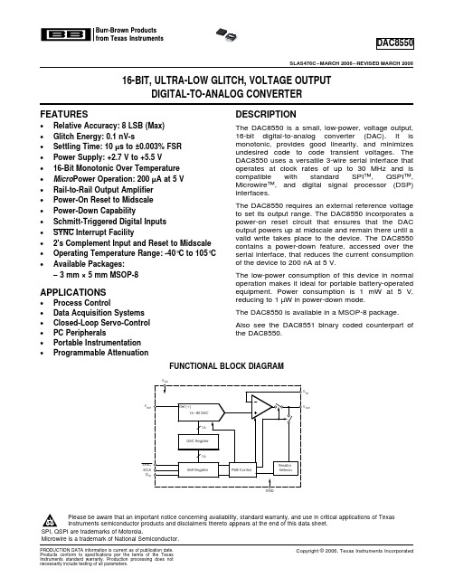
BurrĆBrown Productsfrom TexasInstrumentsFEATURES DESCRIPTIONAPPLICATIONSOUTFBDAC8550SLAS476C–MARCH2006–REVISED MARCH2006 16-BIT,ULTRA-LOW GLITCH,VOLTAGE OUTPUTDIGITAL-TO-ANALOG CONVERTER•Relative Accuracy:8LSB(Max)The DAC8550is a small,low-power,voltage output,16-bit digital-to-analog converter(DAC).It is •Glitch Energy:0.1nV-smonotonic,provides good linearity,and minimizes •Settling Time:10µs to±0.003%FSRundesired code to code transient voltages.The •Power Supply:+2.7V to+5.5V DAC8550uses a versatile3-wire serial interface that •16-Bit Monotonic Over Temperature operates at clock rates of up to30MHz and iscompatible with standard SPI™,QSPI™,•Micro Power Operation:200µA at5VMicrowire™,and digital signal processor(DSP)•Rail-to-Rail Output Amplifier interfaces.•Power-On Reset to MidscaleThe DAC8550requires an external reference voltage •Power-Down Capability to set its output range.The DAC8550incorporates a •Schmitt-Triggered Digital Inputs power-on reset circuit that ensures that the DACoutput powers up at midscale and remain there until a •SYNC Interrupt Facilityvalid write takes place to the device.The DAC8550•2's Complement Input and Reset to Midscale contains a power-down feature,accessed over the•Operating Temperature Range:-40°C to105°C serial interface,that reduces the current consumptionof the device to200nA at5V.•Available Packages:–3mm×5mm MSOP-8The low-power consumption of this device in normaloperation makes it ideal for portable battery-operatedequipment.Power consumption is1mW at5V,reducing to1µW in power-down mode.•Process ControlThe DAC8550is available in a MSOP-8package.•Data Acquisition Systems•Closed-Loop Servo-Control Also see the DAC8551binary coded counterpart of •PC Peripherals the DAC8550.•Portable Instrumentation•Programmable AttenuationFUNCTIONAL BLOCK DIAGRAMPlease be aware that an important notice concerning availability,standard warranty,and use in critical applications of TexasInstruments semiconductor products and disclaimers thereto appears at the end of this data sheet.SPI,QSPI are trademarks of Motorola.Microwire is a trademark of National Semiconductor.PRODUCTION DATA information is current as of publication date.Copyright©2006,Texas Instruments Incorporated Products conform to specifications per the terms of the TexasInstruments standard warranty.Production processing does notnecessarily include testing of all parameters.ABSOLUTE MAXIMUM RATINGS (1)ELECTRICAL CHARACTERISTICSDAC8550SLAS476C–MARCH 2006–REVISED MARCH 2006This integrated circuit can be damaged by ESD.Texas Instruments recommends that all integrated circuits be handled with appropriate precautions.Failure to observe proper handling and installation procedures can cause damage.ESD damage can range from subtle performance degradation to complete device failure.Precision integrated circuits may be more susceptible to damage because very small parametric changes could cause the device not to meet its published specifications.PACKAGING/ORDERING INFORMATIONRELATIVE DIFFERENTIAL SPECIFICATION TRANSPORT PACKAGE PACKAGE PACKAGE ORDERING PRODUCTACCURACYNONLINEARITYTEMPERATUREMEDIA,LEAD DESIGNATOR (1)MARKINGNUMBER (LSB)(LSB)RANGE QUANTITY DAC8550IDGKT Tape and Reel,250DAC8550±12±1MSOP-8DGK–40°C TO 105°CD80DAC8550IDGKR Tape and Reel,2500DAC8550IBDGKT Tape and Reel,250DAC8550B ±8±1MSOP-8DGK –40°C TO 105°C D80DAC8550IBDGKRTape and Reel,2500(1)For the most current package and ordering information,see the Package Option Addendum at the end of this document or see the TI website at .UNITSupply voltage,V DD to GND–0.3V to 6V Digital input voltage range,V I to GND –0.3V to +V DD +0.3V Output voltage,V OUT to GND–0.3V to +V DD +0.3VOperating free-air temperature range,T A –40°C to 105°C Storage temperature range,T STG –65°C to 150°CJunction temperature range,T J(max)150°C Power dissipation (DGK package)(T J max –T A )/θJAThermal impedance,θJA 206°C/W Thermal impedance,θJC44°C/W(1)Stresses above those listed under absolute maximum ratings may cause permanent damage to the device.Exposure to absolute maximum conditions for extended periods may affect device reliability.V DD =2.7V to 5.5V,–40°C to 105°C range (unless otherwise noted)PARAMETERTEST CONDITIONSMINTYPMAXUNITSTATIC PERFORMANCE (1)Resolution16Bits Measured by line passing DAC8550±5±12LSB E L Relative accuracy through codes -32283and ±3±8LSB DAC8550B32063E D Differential nonlinearity 16-bit Monotonic±0.25±1LSB E O Zero-code error ±2±12mV Measured by line passing through codes -32283E FS Full-scale error ±0.05±0.5%of FSR and 32063.E GGain error±0.02±0.2%of FSR Zero-code error drift ±5µV/°C Gain temperature coefficient±1ppm of FSR/°C PSRR Power supply rejection ratio R L =2k Ω,C L =200pF0.75mV/V OUTPUT CHARACTERISTICS (2)V OOutput voltage rangeV REF V(1)Linearity calculated using a reduced code range of -32283to 32063;output unloaded.(2)Specified by design and characterization,not production tested.2Submit Documentation FeedbackDAC8550 SLAS476C–MARCH2006–REVISED MARCH2006ELECTRICAL CHARACTERISTICS(continued)V DD=2.7V to5.5V,–40°C to105°C range(unless otherwise noted)PARAMETER TEST CONDITIONS MIN TYP MAX UNITTo±0.003%FSR,1200H to8D00H,R L=2kΩ,0810µspF<C L<200pFt sd Output voltage settling timeR L=2kΩ,C L=500pF12µsSR Slew rate 1.8V/µsR L=∞470pF Capacitive load stabilityR L=2kΩ1000pFCode change glitch impulse1LSB change around major carry0.1nV-s Digital feedthrough SCLK toggling,FSYNC high0.1z o DC output impedance At mid-code input1ΩV DD=5V50I OS Short-circuit current mAV DD=3V20Coming out of power-down mode V DD=5V 2.5t on Power-up timeµsComing out of power-down mode V DD=3V5AC PERFORMANCESignal-to-noise ratio(1st1995SNRharmonics removed)THD Total harmonic distortion85BW=20kHz,V DD=5V,f OUT=1kHz dBSFDR Spurious-free dynamic range87SINAD Signal-to-noise and distortion84REFERENCE INPUTV ref Reference voltage0V DD VV REF=V DD=5V5075µAI I(ref)Reference current input rangeV REF=V DD=3.6V3045µAz I(ref)Reference input impedance125kΩLOGIC INPUTS(3)Input current±1µAV DD=5V0.8V IL Low-level input voltage VV DD=3V0.6V DD=5V 2.4V IH High-level input voltage VV DD=3V 2.1Pin capacitance3pF POWER REQUIREMENTSV DD 2.7 5.5VI DD(normal mode)Input code equals mid-scale,reference currentincluded,no loadV DD=3.6V to5.5V200250V IH=V DD and V IL=GNDµA V DD=2.7V to3.6V180240I DD(all power-down modes)V DD=3.6V to5.5V V IH=V DD and V IL=GND0.22µA V DD=2.7V to3.6V0.052POWER EFFICIENCYI OUT/I DD I LOAD=2mA,V DD=5V89%TEMPERATURE RANGESpecified performance–40105°C(3)Specified by design and characterization,not production tested.3Submit Documentation Feedback PIN CONFIGURATIONVDDVREFVFBVOUTGNDDINSCLKSYNC 12348765DAC8550DAC8550SLAS476C–MARCH2006–REVISED MARCH2006MSOP-8(Top View)PIN DESCRIPTIONSPIN NAME DESCRIPTION1V DD Power supply input,2.7V to5.5V.2V REF Reference voltage input.3V FB Feedback connection for the output amplifier.4V OUT Analog output voltage from DAC.The output amplifier has rail-to-rail operation.Level-triggered control input(active LOW).This is the frame synchronization signal for the input data.When SYNC goesLOW,it enables the input shift register and data is transferred in on the falling edges of the following clocks.The DAC is 5SYNCupdated following the24th clock(unless SYNC is taken HIGH before this edge in which case the rising edge of SYNC actsas an interrupt and the write sequence is ignored by the DAC8550).6SCLK Serial clock input.Data can be transferred at rates up to30MHz.7D IN Serial data input.Data is clocked into the24-bit input shift register on each falling edge of the serial clock input.8GND Ground reference point for all circuitry on the part.4Submit Documentation FeedbackTIMING REQUIREMENTS(1)(2)SERIAL WRITE OPERATION SYNCDINDAC8550 SLAS476C–MARCH2006–REVISED MARCH2006VDD=2.7V to5.5V,all specifications–40°C to105°C(unless otherwise noted)PARAMETER TEST CONDITIONS MIN TYP MAX UNITV DD=2.7V to3.6V20t c(3)SCLK cycle time nsV DD=3.6V to5.5V20V DD=2.7V to3.6V13t1SCLK HIGH time nsV DD=3.6V to5.5V13V DD=2.7V to3.6V22.5t2SCLK LOW time nsV DD=3.6V to5.5V13V DD=2.7V to3.6V0t su1SYNC to SCLK rising edge setup time nsV DD=3.6V to5.5V0V DD=2.7V to3.6V5t su2Data setup time nsV DD=3.6V to5.5V5V DD=2.7V to3.6V 4.5t h Data hold time nsV DD=3.6V to5.5V 4.5V DD=2.7V to3.6V0t f SCLK falling edge to SYNC rising edge nsV DD=3.6V to5.5V0V DD=2.7V to3.6V50t3Minimum SYNC HIGH time nsV DD=3.6V to5.5V33(1)All input signals are specified with t R=t F=3ns(10%to90%of V DD)and timed from a voltage level of(V IL+V IH)/2.(2)See Serial Write Operation timing diagram.(3)Maximum SCLK frequency is30MHz at V DD=3.6V to5.5V and20MHz at V DD=2.7V to3.6V.5Submit Documentation FeedbackTYPICAL CHARACTERISTICS:V DD =5VL E − (L S B )Digital Input CodeD LE − (L S B )L E − (L S B )819216384245763276840960491525734465536Digital Input CodeD LE − (L S B )−6−4−20246L E − (L S B )−1−0.500.510819216384245763276840960491525734465536Digital Input CodeD LE − (L S B )−50510−404080120Temperature − 5CE r r o r (m V )120140160180200220240260280300I DD − Supply Current − m Af − F r e q u e n c y − H z−10−5−404080120Temperature − 5CE r r o r (m V )DAC8550SLAS476C–MARCH 2006–REVISED MARCH 2006At T A =25°C,unless otherwise noted.Unsigned binary equivalent inputs are shown in all figures.LINEARITY ERROR ANDLINEARITY ERROR ANDDIFFERENTIAL LINEARITY ERROR vs DIGITAL INPUTDIFFERENTIAL LINEARITY ERROR vs DIGITAL INPUTCODE CODE (-40°C)(25°C)Figure 1.Figure 2.LINEARITY ERROR ANDZERO-SCALE ERRORDIFFERENTIAL LINEARITY ERROR vs DIGITAL INPUTvsCODE TEMPERATURE(105°C)Figure 3.Figure 4.FULL-SCALE ERRORI DD HISTOGRAMvsTEMPERATUREFigure 5.Figure 6.6Submit Documentation FeedbackI (SOURCE/SINK) − mA0123456− O u t p u t V o l t a g e − VV O U TDigital Input CodeD D I S u p p l y C u r r e n t − −AµQ u i e s c e n t C u r r en t − Aµ050100150200250−40−10205080110Temperature − 5CD D I S u p p l y C u r r e n t − −AµV DD − Supply Voltage − VIAµV DD − Supply Voltage − VD D− S u p p l y C u r r e n t−1005009001300170012345D D I S u p p l y C u r r e n t − −AµV (LOGIC) − VDAC8550SLAS476C–MARCH 2006–REVISED MARCH 2006TYPICAL CHARACTERISTICS:V DD =5V (continued)At T A =25°C,unless otherwise noted.Unsigned binary equivalent inputs are shown in all figures.SOURCE AND SINK CURRENT CAPABILITYSUPPLY CURRENTvsDIGITAL INPUT CODEFigure 7.Figure 8.POWER-SUPPLY CURRENTSUPPLY CURRENTvsvsTEMPERATURESUPPLY VOLTAGEFigure 9.Figure 10.POWER-DOWN CURRENTSUPPLY CURRENTvsvsSUPPLY VOLTAGELOGIC INPUT VOLTAGEFigure 11.Figure 12.7Submit Documentation FeedbackTime (2 µs/div)V DD = 5 V,V REF = 4.096 V,From Code: FFFF T o Code: 0000Zoomed Falling Edge 1 mV/divTrigger Pulse 5 V/divFalling Edge 1 V/divTime (2 µs/div)V DD = 5 V,V REF = 4.096 V,From Code: 0000T o Code: FFFFZoomed Rising Edge 1 mV/divTrigger Pulse 5 V/divRising Edge 1 V/divTime (2 µs/div)V DD = 5 V,V REF = 4.096 V,From Code: 4000T o Code: CFFFZoomed Rising Edge 1 mV/divTrigger Pulse 5 V/divRising Edge 1 V/divTime (2 µs/div)V DD = 5 V,V REF = 4.096 V,From Code: CFFF T o Code: 4000Zoomed Falling Edge 1 mV/divTrigger Pulse 5 V/divFalling Edge 1 V/divV DD = 5 V,V REF = 4.096 V From Code: 8000T o Code: 7FFF Glitch: 0.16 nV-sMeasured Worst CaseTime 400 ns/divV O U T (500m V /d i v )V DD = 5 V,V REF = 4.096 V From Code: 7FFF T o Code: 8000Glitch: 0.08 nV-sTime 400 ns/divV O U T (500m V /d i v )DAC8550SLAS476C–MARCH 2006–REVISED MARCH 2006TYPICAL CHARACTERISTICS:V DD =5V (continued)At T A =25°C,unless otherwise noted.Unsigned binary equivalent inputs are shown in all figures.FULL-SCALE SETTLING TIME:5-V RISING EDGEFULL-SCALE SETTLING TIME:5-V FALLING EDGEFigure 13.Figure 14.HALF-SCALE SETTLING TIME:5-V RISING EDGEHALF-SCALE SETTLING TIME:5-V FALLING EDGEFigure 15.Figure 16.GLITCH ENERGY:5-V,1-LSB STEP,RISING EDGEGLITCH ENERGY:5-V,1-LSB STEP,FALLING EDGEFigure 17.Figure 18.8Submit Documentation FeedbackV DD = 5 V,V REF = 4.096 V From Code: 8010T o Code: 8000Glitch: 0.08 nV-sTime 400 ns/divV O U T (500V /d i v )m V DD = 5 V,V REF = 4.096 V From Code: 8000T o Code: 8010Glitch: 0.04 nV-sTime 400 ns/divV O U T (500m V /d i v )V DD = 5 V,V REF = 4.096 V From Code: 80FF T o Code: 8000Glitch: Not Detected Theoretical Worst CaseTime 400 ns/divV O U T (5 m V /d i v )V DD = 5 V,V REF = 4.096 V From Code: 8000T o Code: 80FFGlitch: Not Detected Theoretical Worst CaseTime 400 ns/divV O U T (5 m V /d i v )8486889092949698S N R − S i g n a l -t o -N o i s e R a t i o − d Bf − Output Frequency − kHz−100−90−80−70−60−50−40012345T H D − T o t a l H a r m o n i c D i s t o r t i o n − d BOutput Tone − kHzDAC8550SLAS476C–MARCH 2006–REVISED MARCH 2006TYPICAL CHARACTERISTICS:V DD =5V (continued)At T A =25°C,unless otherwise noted.Unsigned binary equivalent inputs are shown in all figures.GLITCH ENERGY:5-V,16-LSB STEP,RISING EDGEGLITCH ENERGY:5-V,16-LSB STEP,FALLING EDGEFigure 19.Figure 20.GLITCH ENERGY:5-V,256-LSB STEP,RISING EDGEGLITCH ENERGY:5-V,256-LSB STEP,FALLING EDGEFigure 21.Figure 22.TOTAL HARMONIC DISTORTIONSIGNAL-TO-NOISE RATIOvsvsOUTPUT FREQUENCYOUTPUT FREQUENCYFigure 23.Figure 24.9Submit Documentation Feedback100150200250300350100100010000100000n V /H z− V o l t a g e N o i s e −V n f − Frequency − Hzf − Frequency − HzG a i n − d BDAC8550SLAS476C–MARCH 2006–REVISED MARCH 2006TYPICAL CHARACTERISTICS:V DD =5V (continued)At T A =25°C,unless otherwise noted.Unsigned binary equivalent inputs are shown in all figures.POWER SPECTRAL DENSITYOUTPUT NOISE DENSITYFigure 25.Figure 26.10Submit Documentation FeedbackTYPICAL CHARACTERISTICS:V DD =2.7VL E − (L S B )Digital Input CodeD LE − (L S B )−6−4−20246L E − (L S B )D LE − (L S B )Digital Input CodeL E − (L S B )Digital Input CodeD LE − (L S B )510Temperature − 5CE r r o r (m V )30060090012001500120140160180200220240260280300I DD − Supply Current − m Af − F r e q u e n c y − H z−10−505Temperature − 5CE r r o r (m V )DAC8550SLAS476C–MARCH 2006–REVISED MARCH 2006At T A =25°C,unless otherwise noted.Unsigned binary equivalent inputs are shown in all figures.LINEARITY ERROR ANDLINEARITY ERROR ANDDIFFERENTIAL LINEARITY ERROR vs DIGITALDIFFERENTIAL LINEARITY ERROR vs DIGITALINPUT CODE INPUT CODE(-40°C)(25°C)Figure 27.Figure 28.LINEARITY ERROR ANDZERO-SCALE ERRORDIFFERENTIAL LINEARITY ERROR vs DIGITAL INPUTvsCODE TEMPERATURE(105°C)Figure 29.Figure 30.FULL-SCALE ERRORI DD HISTOGRAMvsTEMPERATUREFigure 31.Figure 32.11Submit Documentation FeedbackI (SOURCE/SINK) − mA− O u t p u t V o l t a g e − VV O U TDigital Input CodeD D I S u p p l y C u r r e n t − −Aµ10030050070000.51 1.52 2.5D D I S u p p l y C u r r e n t − −AµV (LOGIC)− VQ u i e s c e n t C u r r e n t − AµTemperature − 5CTime (2 µs/div)V DD = 2.7 V,V REF = 2.5 V,From Code: 0000T o Code: FFFFZoomed Rising Edge 1 mV/divTrigger Pulse 2.7 V/divRising Edge 0.5 V/divV DD = 2.7 V,V REF = 2.5 V,From Code: FFFF T o Code: 0000Zoomed Falling Edge 1 mV/divTrigger Pulse 2.7 V/divFalling Edge 0.5 V/divTime (2 µs/div)DAC8550SLAS476C–MARCH 2006–REVISED MARCH 2006TYPICAL CHARACTERISTICS:V DD =2.7V (continued)At T A =25°C,unless otherwise noted.Unsigned binary equivalent inputs are shown in all figures.SOURCE AND SINK CURRENT CAPABILITYSUPPLY CURRENTvsDIGITAL INPUT CODEFigure 33.Figure 34.POWER-SUPPLY CURRENTSUPPLY CURRENTvsvsTEMPERATURELOGIC INPUT VOLTAGEFigure 35.Figure 36.FULL-SCALE SETTLING TIME:2.7-V RISING EDGEFULL-SCALE SETTLING TIME:2.7-V FALLING EDGEFigure 37.Figure 38.12Submit Documentation FeedbackTrigger Pulse 2.7 V/divZoomed Rising Edge 1 mV / divV DD = 2.7 V V REF = 2.5 V From code; 4000T o code: CFFFRising Edge 0.5 V/divTime − 2 m s/div V DD = 2.7 V,V REF = 2.5 V,From Code: CFFF T o Code: 4000Zoomed Falling Edge 1 mV/divTrigger Pulse 2.7 V/divFalling Edge 0.5 V/divTime (2 µs/div)V DD = 2.7 V,V REF = 2.5 VFrom Code: 7FFF T o Code: 8000Glitch: 0.08 nV-sTime 400 ns/div V O U T (200 m V /d i v )V DD = 2.7 V,V REF = 2.5 V From Code: 8000T o Code: 7FFF Glitch: 0.16 nV-sMeasured Worst CaseTime 400 ns/divV O U T (200 m V /d i v )V DD = 2.7 V,V REF = 2.5 V From Code: 8000T o Code: 8010Glitch: 0.04 nV-sTime 400 ns/divV O U T (200 u V /d i v )V DD = 2.7 V,V REF = 2.5 V From Code: 8010T o Code: 8000Glitch: 0.12 nV-sTime 400 ns/divV /d i v )V O U T (200 u V /d i v )DAC8550SLAS476C–MARCH 2006–REVISED MARCH 2006TYPICAL CHARACTERISTICS:V DD =2.7V (continued)At T A =25°C,unless otherwise noted.Unsigned binary equivalent inputs are shown in all figures.HALF-SCALE SETTLING TIME:2.7-V RISING EDGEHALF-SCALE SETTLING TIME:2.7-V FALLING EDGEFigure 39.Figure 40.GLITCH ENERGY:2.7-V,1-LSB STEP,RISING EDGEGLITCH ENERGY:2.7-V,1-LSB STEP,FALLING EDGEFigure 41.Figure 42.GLITCH ENERGY:2.7-V,16-LSB STEP,RISING EDGEGLITCH ENERGY:2.7-V,16-LSB STEP,FALLING EDGEFigure 43.Figure 44.13Submit Documentation FeedbackV DD = 2.7 V,V REF = 2.5 VFrom Code: 80FF T o Code: 8000Glitch: Not Detected Theoretical Worst CaseTime 400 ns/divV O U T (5 m V /d i v )AV DD = 2.7 V,V ref = 2.5 VFrom Code: 8000T o Code: 80FFGlitch: Not Detected Theoretical Worst CaseTime 400 ns/divV O U T (5 m V /d i v )DAC8550SLAS476C–MARCH 2006–REVISED MARCH 2006TYPICAL CHARACTERISTICS:V DD =2.7V (continued)At T A =25°C,unless otherwise noted.Unsigned binary equivalent inputs are shown in all figures.GLITCH ENERGY:2.7-V,256-LSB STEP,RISING EDGEGLITCH ENERGY:2.7-V,256-LSB STEP,FALLING EDGEFigure 45.Figure 46.14Submit Documentation FeedbackTHEORY OF OPERATION DAC SECTIONV OUT*V REF2)V REF D65536(1)To OutputAmplifierRESISTOR STRINGSERIAL INTERFACE OUTPUT AMPLIFIER DAC8550SLAS476C–MARCH2006–REVISED MARCH2006 The architecture consists of a string DAC followed byan output buffer amplifier.Figure47shows the blockdiagram of the DACFigure47.DAC8550ArchitectureThe input coding to the DAC8550is2's complement,so the ideal output voltage is given by:where D=decimal equivalent of the2's complementcode that is loaded to the DAC register;D rangesfrom-32768to+32767where D=0is centered atV REF/2.Figure48.Resistor StringThe resistor string section is shown in Figure48.It issimply a string of resistors,each of Thecode loaded into the DAC register determines atwhich node on the string the voltage is tapped off toThe DAC8550has a3-wire serial interface(SYNC, be fed into the output amplifier by closing one of theSCLK,and D IN),which is compatible with SPI™, switches connecting the string to the amplifier.QSPI™,and Microwire™interface standards,as well Monotonicity is ensured due to the string resistoras most DSP interfaces.See the Serial Write architecture.Operation timing diagram for an example of a typicalwrite sequence.The write sequence begins by bringing the SYNC line The output buffer amplifier is capable of generatingLOW.Data from the D IN line is clocked into the24-bit rail-to-rail output voltages with a range of0V to V DD.shift register on each falling edge of SCLK.The serial It is capable of driving a load of2Ωk in parallel withclock frequency can be as high as30MHz,making 1000pF to GND.The source and sink capabilities ofthe DAC8550compatible with high-speed DSPs.On the output amplifier can be seen in the typical curves.the24th falling edge of the serial clock,the last data The slewrate is1.8V/µs with a full-scale setting timebit is clocked in and the programmed function is of8µs with the output unloaded.excuted(i.e.,a change in DAC register contents The inverting input of the output amplifier is brought and/or a change in the mode of operation).out to the V FB pin.This allows for better accuracy inAt this point,the SYNC line may be kept LOW or critical applications by tying the V FB point and thebrought HIGH.In either case,it must be brought amplifier output together directly at the load.OtherHIGH for a minimum of33ns before the next write signal conditioning circuitry may also be connectedsequence so that a falling edge of SYNC can initiate between these points for specific applications.the next write sequence.Since the SYNC bufferdraws more current when the SYNC signal is HIGH15Submit Documentation FeedbackSYNC INTERRUPTINPUT SHIFT REGISTERPOWER-ONRESETCLK D INValid Write Sequence: Output Updateson the 24th Falling Edge24th Falling Edge24th Falling EdgeDB23DB80DB23DB80POWER-DOWN MODESDAC8550SLAS476C–MARCH 2006–REVISED MARCH 2006than it does when it is LOW,SYNC should be idled LOW between write sequences for lowest power In a normal write sequence,the SYNC line is kept operation of the part.As mentioned above,it must be LOW for at least 24falling edges of SCLK and the brought HIGH again just before the next write DAC is updated on the 24th falling edge.However,if sequence.SYNC is brought HIGH before the 24th falling edge,it acts as an interrupt to the write sequence.The shift register is reset and the write sequence is seen as invalid.Neither an update of the DAC register The input shift register is 24bits wide,as shown in contents nor a change in the operating mode occurs,Figure 49.The first six bits are don't care bits.The as shown in Figure 50.bits (PD1andPD0)are control bits that control which mode of operation the part is in (normal mode or any one of three power-down modes).For a more complete description of the various modes see The DAC8550contains a power-on reset circuit that the Power-Down Modes section.The next 16bits are controls the output voltage during power-up.On the data bits.These are transferred to the DAC power-up,the output voltages are set to midscale;it register on the 24th falling edge of SCLK.remains there until a valid write sequence is made to the DAC.This is useful in applications where it is important to know the state of the output of the DAC while it is in the process of powering up.XXXXXXPD1PD0D15D14D13D12D11D10D9D8D7D6D5D4D3D2D1D0Figure 49.DAC8550Data Input Register FormatFigure 50.SYNC Interrupt Facilityat 5V.However,for the three power-down modes,the supply current falls to 200nA at 5V (50nA at 3V).Not only does the supply current fall,but the The DAC8550supports four seperate modes of output stage is also internally switched from the operation.These modes are programmable by setting output of the amplifier to a resistor network of known two bits (PD1and PD0)in control register.Table 1values.The advantage with this is that the output shows how the state of the bits corresponds to the impedance of the device is known while in mode of operation of the device.power-down mode.There are three different options.The output is connected internally to GND through a Table 1.Modes of Operation for the DAC85501-k Ωresistor,a 100-k Ωresistor,or it is left open-circuited (High-Z).The output stage is illustrated PD1PD0OPERATING MODE(DB17)(DB16)in Figure 51.00Normal operation All analog circuitry is shut down when the ----Power-down modespower-down mode is activated.However,the 01Output typically 1k Ωto GND contents of the DAC register are unaffected when in power-down.The time to exit power-down is typically 10Output typically 100k Ωto GND 2.5µs for V DD =5V,and 5µs for V DD =3V.See the 11High-ZTypical Characteristics for more information.When both bits are set to 0,the device works normally with a typical current consumption of 200µA16Submit Documentation FeedbackDAC8550to Microwire InterfaceOUTFBNOTE: (1)Additional pins omitted for clarity.MICROPROCESSOR INTERFACINGDAC8550TO 8051InterfaceDAC8550to 68HC11InterfaceNOTE: (1)Additional pins omitted for clarity.NOTE: (1)Additional pins omitted for clarity.DAC8550SLAS476C–MARCH 2006–REVISED MARCH 2006Figure 53shows an interface between the DAC8550compatible device.Serial data is shifted out on the falling edge of the serial clock and is clocked into the DAC8550on the rising edge of the SK signal.Figure 51.Output Stage During Power-DownFigure 53.DAC8550to Microwire Interface See Figure 52for a serial interface between the Figure 54shows a serial interface between the a typical 8051-type microcontroller.and the 68HC11microcontroller.SCK of The setup for the interface is as follows:TXD of the the 68HC11drives the SCLK of the DAC8550,while 8051drives SCLK of the DAC8550,while RXD drives the MOSI output drives the serial data line of the the serial data line of the device.The SYNC signal is DAC.The SYNC signal is derived from a port line derived from a bit-programmable pin on the port of (PC7),similar to the 8051diagram.the 8051.In this case,port line P3.3is used.When data is to be transmitted to the DAC8550,P3.3is taken LOW.The 8051transmits data in 8-bit bytes;thus only eight falling clock edges occur in the transmit cycle.To load data to the DAC,P3.3is left LOW after the first eight bits are transmitted,then a second write cycle is initiated to transmit the second byte of data.P3.3is taken HIGH following the completion of the third write cycle.The 8051outputs Figure 54.DAC8550to 68HC11Interface the serial data in a format which has the LSB first.The DAC8550requires its data with the MSB as the first bit received.The 8051transmit routine must The 68HC11should be configured so that its CPOL therefore take this into account,and mirror the data bit is 0and its CPHA bit is 1.This configuration as needed.causes data appearing on the MOSI output to be valid on the falling edge of SCK.When data is being transmitted to the DAC,the SYNC line is held LOW (PC7).Serial data from the 68HC11is transmitted in 8-bit bytes with only eight falling clock edges occurring in the transmit cycle.(Data is transmitted MSB first.)In order to load data to the DAC8550,PC7is left LOW after the first eight bits are transferred,then a second and third serial write Figure 52.DAC8550to 80C51/80L51Interfaceoperation is performed to the DAC.PC7is taken HIGH at the end of this procedure.17Submit Documentation Feedback。
超级芯片应用电路汇总

76810机心电路分析与检修76810机心是三洋公司最新推出的以单片式集成电路LA76810为大规模小信号处理电路为主的机心,LA76810内部包括图象/伴音中频处理、亮度/色度信号处理、行/场偏转小信号处理电路等,不需外接1H基带延迟线。
当需要处理SECAM制信号时,只要外接一只免调试SECAM解调电路LA7642即可。
本机心功能的控制采用相应的三洋公司微处理芯片LC863348A经I2C总线来完成,是一款性价比高、性能优越的彩电机心之一。
采用此机心的海尔牌HT-2199D型彩电是此系列机心中的一款,本文以HT-2199D彩电为例分析该机心的电路及典型故障的检修。
一.HT-2199D彩电的电路组成框图、主要集成电路和信号流程1.HT-2199D彩电的电路组成框图如图一所示。
2.HT-2199D彩电采用的主要集成电路见表1。
表1HT-2199D彩电主要集成电路一览表位号型号主要功能引脚数N801LC863348A微处理器42N802AT24C04存储器8N201LC76810单片小信号处理54N501LA7840场扫描输出7N131TDA1013B伴音功放9N001HEF4053TV/AV转换16N652L78M12+12V稳压3N653L78M05+5V稳压33.信号流程参阅图一。
从天线接收的高频电视信号在调谐器中经高频放大、混频处理后变成中频信号,经预中放和声表面波滤波器放大和选频,进入N201进行处理。
本机小信号处理全部在N201内完成。
图象中频信号经图象中放电路放大、同步检波电路解调,得到视频信号和伴音中频信号。
伴音中频信号回到N201中进行限幅放大及调频检波,解调成音频信号,再经过N131的音量控制和功率放大,推动扬声器发声。
视频信号也回到N201中进行PAL/NTSC制彩色解码,得到R、G、B基色信号,再进入末级视频放大器进行放大激励显象管三阴极。
AV端子的视频信号与S端子的亮度信号Y和色度信号C在视频开关N001中进行切换选择,将选中的视频信号送至N201中,完成彩色解码等功能。
I-H开头的集成电路

HES8455 色度信号处理集成电路
HG5402 开关电源厚膜集成电路
HG6576 电机稳速控制集成电路
HIC1015 开关电源控制集成电路
HIC1016 开关电源控制集成电路
HM006 音频前置放大集成电路
HM4864P-12 存储集成电路
HM4868P-12 存储集成电路
HT9202D 拨号控制集成电路
HT9202G 拨号控制集成电路
HT9202L 拨号控制集成电路
HY403 电子音乐集成电路
HY514260B 动态存储集成电路
HY57V161610ATC-10 存储16M集成电路
HY62256ALJ-70-TR 存储集成电路
HYB514171BJ 存储集成电路
HT1613 液晶显示驱动集成电路
HT1613A 液晶显示驱动集成电路
HT1616A 液晶显示驱动集成电路
HT4207-4L 频率调制集成电路
HT4238-4L 频率解调集成电路
HT4239-4L 色度信号处理集成电路
HT4664A-IE15 重放亮度信号处理集成电路
HT4848B 亮度信号处理集成电路
HA12102 双声道前置放大集成电路
HA12158NT 伺服信号处理集成电路
HA12196NT 录放音信号处理集成电路
HA12413 调频/调幅中频放大集成电路
HA13001 音频功率放大5.5W×2集成电路
HA1308 音频功率放大集成电路
HA1314 音频功率放大1W集成电路
HA1339A 音频功率放大集成电路
IX0412CE 字符发生集成电路
MXL608规格书

Date Code:
YYWW
MXL608 BBBBB.XX YYWW CC
AAA = Maxlineaห้องสมุดไป่ตู้ part number BBBBB. XX = Assembly lot number YY = Year WW = Work week CC = MaxLinear Internal Code
7MHz, and 8MHz ■ Low power consumption with 3.3V and 1.8V
dual-supply operation ■ On-chip voltage regulator for 3.3V operation
with single supply ■ Programmable IF frequency and IF spectrum
Figure 1
1.2 Ordering Part Number:
MXL608 – A G – T
Tray 4x4mm QFN Standard product MaxLinear part number
1.3 Assembly Location: ASE, Chung-Li, Taiwan
MxL608 Marking
Data Sheet
MxL608
Digital Cable and Terrestrial Silicon Tuner
General Description
The MxL608 is a highly integrated, low power silicon tuner IC that targets low-cost digital terrestrial and digital cable Set-Top Box (STB) applications.
昂科烧录器更新支持HDSC华大半导体的HC32L072系列32位微控制器HC32L072KAT的烧录

昂科发布软件更新支持HDSC华大半导体的HC32L072系列32位微控制器HC32L072KAT的烧录芯片烧录行业领导者-昂科技术近日发布最新的烧录软件更新及新增支持的芯片型号列表,其中昂科发布软件更新支持HDSC华大半导体的HC32L072系列32位微控制器HC32L072KAT的烧录已经被昂科的通用烧录平台AP8000所支持。
HC32L072系列是一款旨在延长便携式测量系统的电池使用寿命的超低功耗、宽电压工作范围的MCU。
集成12位1Msps高精度SARADC,2个12位DAC以及集成了比较器、运放、内置高性能PWM定时器、LCD显示、多路UART、SPI、I2C、I2S、USB、CAN等丰富的通讯外设,内建AES、TRNG等信息安全模块,具有高整合度、高抗干扰、高可靠性和超低功耗的特点。
本产品内核采用Cortex-M0+内核,配合成熟的Keil & IAR调试开发软件,支持C语言及汇编语言,汇编指令。
超低功耗MCU典型应用•传感器应用、物联网应用•智能仪表、无线模块、温控器、货架标签•智能交通、报警系统•智能家居、医疗设备产品特性•48MHz Cortex-M0+ 32位CPU平台•HC32L072系列具有灵活的功耗管理系统–1.2μA@3V深度休眠模式:所有时钟关闭,上电复位有效,IO状态保持,IO中断有效,所有寄存器、RAM和CPU数据保存状态时的功耗–1.6μA@3V深度睡眠模式+RTC工作–9μ***********低速工作模式:CPU运行,外设关闭,从FLASH运行程序–40μA/MHz@3V@24MHz休眠模式:CPU停止,外设关闭,主时钟运行–140μA/MHz@3V@24MHz工作模式:CPU运行,外设关闭,从FLASH运行程序–4μs唤醒时间,使模式切换更加灵活高效,系统反应更为敏捷•128K字节FLASH存储器,具有擦写保护功能,支持ISP、ICP、IAP•16K字节RAM存储器,附带奇偶校验,增强系统的稳定性•通用I/O管脚•时钟、晶振–外部高速晶振4~32MHz–外部低速晶振32.768kHz–内部高速时钟4/8/16/22.12/24MHz–内部低速时钟32.8/38.4kHz–PLL时钟8~48MHz–内部高US时钟48MHz–硬件支持内外时钟校准和监控•定时器/计数器–3个通用16位定时器,支持1组互补PWM输出,支持2倍主频PWM输出,最高支持96MHz PWM输出–1个高级16位定制器,支持3相互补PWM输出,支持2倍主频PWM输出,最高支持96MHz PWM输出–3个高性能16位定时器/计数器,支持PWM互补,死区保护功能–1个超低功耗脉冲计数器PCNT,具备低功耗模式下自动定时唤醒功能,最大定时达1024秒–1个可编程16位定时器PCA,支持5通道捕获比较,5通道PWM输出–2个低功耗16位定时器,支持级联–1个20位可编程看门狗电路,内建专用10kHz振荡器提供WDT计数•通讯接口–4路UART标准通讯接口–2路LPUART低功耗通讯接口,深度休眠模式下可工作–2路SPI标准通讯接口–2路I2C标准通讯接口–2路I2S音频通信接口–1路Crystal-less USB Full Speed Device–1路CAN 2.0B标准通讯接口•蜂鸣器频率发生器,支持互补输出•硬件万年历RTC模块•硬件CRC-16/32模块•硬件32位除法器•AES-128/192/256硬件协处理器•TRNG真随机数发生器•2通道DMAC•全球唯一10字节ID号•12位1Msps采样的高速高精度SARADC,内置运放,可测量高输出阻抗的信号•2路12位500Ksps DAC•集成5个多功能运算放大器,其中两个OPA可以作为2路DAC的输出Buffer •集成3路电压比较器,具有6位DAC和可编程比较基准•集成低电压侦测器,可配置16阶比较电压,可监控端口电压以及电源电压•SWD调试解决方案,提供全功能调试器•工作条件:-40~85℃,1.8~5.5V功能框图昂科技术自主研发的AP8000万用型烧录器包含主机,底板,适配座三大部分。
【2017年整理】DAC解码芯片的泰斗
DAC解码芯片的泰斗---转目前,烧友们对DIY/DAC解码器风头正劲,近日从一朋友那里弄来一些关于DAC解码芯片的资料,愿与大家分享。
DAC芯片通常由Crystal、Burr Brown、AKM、Analog这4家公司包揽。
Burr Brown公司隶属于半导体业界著名的重量级厂家德州仪器公司,其最为人熟知的DAC 芯片莫过于PCM1704。
众多Hi End厂家都对其大加赞赏,其中包括不少坚持传统两声道的Hi End厂家,如Mark Levinson最顶级的解码器NO.360(4495美元)就采用了PCM1704。
它是一块精密的24bit D/A转换芯片,拥有超低失真和低电平响应线性。
其采用了2μm BICMOS制造工艺和一种非常独特的示意数量型架构(Sign Magnitude)。
在其内部设计了两个23bit完全互补的D/A转换器,从而取得24bit的精度。
这两个D/A转换器公用一个时钟参考,公用一个R 2R型梯形电阻网络,通过不断分压来取得准确的数位电流源信号。
R 2R梯形电阻网络使用的双平衡电流回路可以确保在任何电平下对电压信号都有理想的跟踪能力。
这两个D/A转换器在内部数据计算上完全独立,可以有非常线性的电平响应,尤其是在低电平(即小音量)下线性良好。
R 2R梯形电阻网络里的电阻都是将镍铬薄膜电阻经激光微调制得的,因此精度足够高。
另外,两个D/A转换器也是经过精密配对才加以使用的。
PCM1704 的信噪比达到了令人惊异的 120dB,并且是标准型 K 级芯片。
其总谐波失真和噪声达到了0.0008%(-101.94 dB),也是标准型K级芯片。
标准型K级的动态范围达到了112dB。
PCM1704的取样频率范围为16~96kHz,过取样频率为96kHz的8倍过取样。
另外,其输入音频数据格式为20bit或24bit,快速电流输出为±1.2mA/200ns,电源电压为±5V。
DS_FT232H
Future Technology Devices International Ltd FT232H Single Channel Hi-Speed USB to MultipurposeUART/FIFO ICThe FT232H is a single channel USB 2.0 Hi-Speed (480Mb/s) to UART/FIFO IC. It has the capability of being configured in a variety of industry standard serial or parallel interfaces. The FT232H has the following advanced features:Single channel USB to serial / parallel ports with a variety of configurations.Entire USB protocol handled on the chip. No USB specific firmware programming required.USB 2.0 Hi-Speed (480Mbits/Second) and Full Speed (12Mbits/Second) compatible.Multi-Protocol Synchronous Serial Engine (MPSSE) to simplify synchronous serial protocol (USB to JTAG, I2C, SPI (MASTER) or bit-bang) design.UART transfer data rate up to 12Mbaud.(RS232 Data Rate limited by external level shifter).USB to asynchronous 245 FIFO mode for transfer data rate up to 8 Mbyte/Sec.USB to synchronous 245 parallel FIFO mode for transfers upto 40 Mbytes/SecSupports a proprietary half duplex FT1248 interface with a configurable width, bi-directional data bus (1, 2, 4 or 8 bits wide).CPU-style FIFO interface mode simplifies CPU interface design.Fast serial interface option.FTDI‟s royalty-free Virtual Com Port (VCP) and Direct (D2XX) drivers eliminate the requirement for USB driver development in most cases.Adjustable receive buffer timeout. Option for transmit and receive LED drive signals.Bit-bang Mode interface option with RD# and WR# strobesHighly integrated design includes 5V to 3.3/+1.8V LDO regulator for VCORE, integrated POR functionAsynchronous serial UART interface option with full hardware handshaking and modem interface signals.Fully assisted hardware or X-On / X-Off software handshaking.UART Interface supports 7/8 bit data, 1/2 stop bits, and Odd/Even/Mark/Space/No Parity.Auto transmit enable control for RS485 serial applications using the TXDEN pin.Operational mode configuration and USB Description strings configurable in external EEPROM over the USB interface.Configurable I/O drives strength (4, 8, 12 or 16mA) and slew rate.Low operating and USB suspend current. Supports self powered, bus powered and high-power bus powered USB configurations.UHCI/OHCI/EHCI host controller compatible. USB Bulk data transfer mode (512 byte packets in Hi-Speed mode).+1.8V (chip core) and +3.3V I/O interfacing (+5V Tolerant).Extended -40°C to 85°C industrial operating temperature range.Compact 48-pin Lead Free LQFP or QFN packageConfigurable ACBUS I/O pins.1Typical ApplicationsSingle chip USB to UART (RS232, RS422 or RS485)USB to FIFOUSB to FT1248USB to JTAGUSB to SPIUSB to I2CUSB to Bit-BangUSB to Fast Serial InterfaceUSB to CPU target interface (as memory) USB InstrumentationUSB Industrial ControlUSB EPOS ControlUSB MP3 Player InterfaceUSB FLASH Card Reader / Writers Set Top Box - USB interfaceUSB Digital Camera Interface USB Bar Code Readers1.1Driver SupportThe FT232H requires USB device drivers (listed below), available free from , to operate. The VCP version of the driver creates a Virtual COM Port allowing legacy serial port applications to operate over USB e.g. serial emulator application TTY. Another FTDI USB driver, the D2XX driver, can also be used with application software to directly access the FT232H through a DLL.Royalty free VIRTUAL COM PORT (VCP) DRIVERS for...Windows 7 and Windows 7 64-bitWindows Vista and Vista 64-bitWindows XP and XP 64-bitWindows XP EmbeddedWindows 2000, Server 2003, Server 2008 Windows CE 4.2, 5.0, 5.2 and 6.0Mac OS-XLinux (2.6.9 or later) Royalty free D2XX Direct Drivers (USB Drivers + DLL S/W Interface) Windows 7 and Windows 7 64-bitWindows Vista and Vista 64-bitWindows XP and XP 64-bitWindows XP EmbeddedWindows 2000, Server 2003, Server 2008 Windows CE 4.2, 5.0, 5.2 and 6.0Mac OS-XLinux (2.6.9 or later)1.2Part NumbersNote: Packaging codes for xxxx is:- Reel: Taped and Reel (LQFP = 1500 pieces per reel, QFN = 3000 pieces per reel) -Tray: Tray packing, (LQFP = 250 pieces per tray, QFN =260 pieces per tray) Please refer to section 8 for all package mechanical parameters.The FT232H is fully compliant with the USB 2.0 specification and has been given the USB-IF Test-ID (TID) 40770005.The timing of the rise/fall time of the USB signals is not only dependant on the USB signal drivers, it is also dependant system and is affected by factors such as PCB layout, external components and any transient protection present on the USB signals. For USB compliance these may require a slight adjustment. This timing can be modified through a programmable setting stored in the same external EEPROM that is used for the USB descriptors. Timing can also be changed by adding appropriate passive components to the USB signals.1.4Applicable DocumentsThe following application and technical documents can be downloaded by clicking on the appropriate links below:AN_108 – Command Processor For MPSSE and MCU Host Bus Emulation ModesAN_113 – Interfacing FT2232H Hi-Speed Devices To I2C BusAN_114 – Interfacing FT2232H Hi-Speed Devices To SPI BusAN_129 – Interfacing FT2232H Hi-Speed Devices to a JTAG TAPAN_135 – MPSSE BasicsAN_167_FT1248 Parallel Serial Interface BasicsFigure 2.1 FT232H Block DiagramA full description of each function is available in section 4.1Typical Applications (2)1.1Driver Support (2)1.2Part Numbers (2)1.3USB Compliant (3)1.4Applicable Documents (3)2FT232H Block Diagram (4)3Device Pin Out And Signal Descriptions (7)3.1Schematic Symbol (7)3.2FT232H Pin Descriptions (8)3.3Signal Description (9)3.4ACBUS Signal Option (12)3.5Pin Configurations (13)3.5.1FT232H pins used in an UART interface (13)3.5.2FT232H pins used in an FT245 Synchronous FIFO Interface (14)3.5.3FT232H pins used in an FT245 Style Asynchronous FIFO Interface (15)3.5.4FT232H can be configured as a Synchronous or Asynchronous Bit-Bang Interface. (16)3.5.5FT232H pins used in an MPSSE (17)3.5.6FT232H Pins used as a Fast Serial Interface (18)3.5.7FT232H Pins Configured as a CPU-style FIFO Interface (19)3.5.8FT232H Pins Configured as a FT1248 Interface (20)4Function Description (21)4.1Key Features (21)4.2Functional Block Descriptions (22)4.3FT232 UART Interface Mode Description (23)4.3.1RS232 Configuration (23)4.3.2RS422 Configuration (24)4.3.3RS485 Configuration (25)4.4FT245 Synchronous FIFO Interface Mode Description (26)4.4.1FT245 Synchronous FIFO Read Operation (27)4.4.2FT245 Synchronous FIFO Write Operation (27)4.5FT245 Style Asynchronous FIFO Interface Mode Description (28)4.6FT1248 Interface Mode Description (29)4.6.1Bus Width Protocol Decode (30)4.6.2FT1248: 1-bit interface (31)4.7Synchronous and Asynchronous Bit-Bang Interface Mode (33)4.7.1Asynchronous Bit-Bang Mode (33)4.7.2Synchronous Bit-Bang Mode (33)4.8.1MPSSE Adaptive Clocking (36)4.9Fast Serial Interface Mode Description (37)4.9.1Outgoing Fast Serial Data (38)4.9.2Incoming Fast Serial Data (38)4.9.3Fast Serial Data Interface Example (39)4.10CPU-style FIFO Interface Mode Description (40)4.11RS232 UART Mode LED Interface Description (42)4.12Send Immediate / Wake Up (SIWU#) (43)4.13FT232H Mode Selection (44)4.14Modes Configurations (45)5Devices Characteristics and Ratings (46)5.1Absolute Maximum Ratings (46)5.2DC Characteristics (47)5.3ESD Tolerance (49)6FT232H Configurations (50)6.1USB Bus Powered Configuration (50)6.2USB Self Powered Configuration (51)6.2.1Self Powered application example 2 (52)6.3Oscillator Configuration (53)7EEPROM Configuration (54)7.1EEPROM Interface (54)7.2Default EEPROM Configuration (55)8Package Parameters (57)8.1FT232HQ, QFN-48 Package Dimensions (57)8.2FT232HL, LQFP-48 Package Dimensions (58)8.3Solder Reflow Profile (59)9Contact Information (61)Appendix A – List of Figures and Tables (63)List of Tables (63)List of Figures (64)Appendix B – Revision History (65)3 Device Pin Out And Signal DescriptionsThe 48-pin LQFP and 48-pin QFN have the same pin numbering for specific functions. This pin numbering is illustrated in the schematic symbol shown in Figure 3.13.1Schematic SymbolFigure 3.1 FT232H Schematic SymbolThis section describes the operation of the FT232H pins. Both the LQFP and the QFN packages have the same function on each pin. The function of many pins is determined by the configuration of the FT232H. The following table details the function of each pin dependent on the configuration of the interface. Each of the functions is described in the following table (Note: The convention used throughout this document for active low signals is the signal name followed by #).Pins marked ** default to tri-stated inputs with an internal 75KΩ (approx) pull up resistor to VCCIO.Pin marked *** default to GPIO line with an internal 75KΩ pull down resistor to GND. Using the EEPROM this pin can be enabled USBVCC mode instead of GPIO mode.** If pin 40 (VREGIN) is +5.0V, pin 39 becomes an output and If pin 40 (VREGIN) is 3V3 pin 39 becomes an input.Table 3.4 UART Interface and ACBUS Group (see note 1)Notes:1. When used in Input Mode, the input pins are pulled to VCCIO via internal 75kΩ (approx) resistors. These pins can be programmed to gently pull low during USB suspend (PWREN# = “1”) by setting anoption in the EEPROM.If the external EEPROM is fitted, the following options can be configured on the CBUS I/O pins using the software utility FT_PROG which can be downloaded from the FTDI utilities page. CBUS signal options are common to both package versions of the FT232H. The default configuration is described in section 7.* Must be used with a 10kΩ resistor pull up.**When in USB suspend mode the outputs clocks are also suspended.The following section describes the function of the pins when the device is configured in different modes of operation.3.5.1FT232H pins used in an UART interfaceThe FT232H can be configured as a UART interface. When configured in this mode, the pins used and the descriptions of the signals are shown in Table 3.6** ACBUS I/O pinsFor a functional description of this mode, please refer to section 4.3NOTE: UART is the device default mode.The FT232H can be configured as a FT245 synchronous FIFO interface. When configured in this mode, the pins used and the descriptions of the signals are shown in Table 3.7. To set this mode the external EEPROM must be set to 245 modes. A software command (FT_SetBitMode) is then sent by the application to the FTDI D2xx driver to tell the chip to enter 245 synchronous FIFO mode. In this mode, data is written or read on the rising edge of the CLKOUT. Refer to Figure 4.4 for timing details.For a functional description of this mode, please refer to section 4.4The FT232H can be configured as a FT245 style asynchronous FIFO interface. When configured in this mode, the pins used and the descriptions of the signals are shown in Table 3.8. To enter this mode the external EEPROM must be set to 245 asynchronous FIFO mode. In this mode, data is written or read on the falling edge of the RD# or WR# signals.For a functional description of this mode, please refer to section 4.5Interface.Bit-bang mode is an FTDI FT232H device mode that changes the 8 IO lines into an 8 bit bi-directional data bus. This mode is enabled by sending a software command (FT_SetBitMode) to the FTDI driver. When configured in any bit-bang mode, the pins used and the descriptions of the signals are shown in Table 3.9For functional description of this mode, please refer to section 4.6The FT232H has a Multi-Protocol Synchronous Serial Engine (MPSSE). This mode is enabled by sending a software command (FT_SetBitMode) to the FTDI D2xx driver. The MPSSE can be configured to a number of industry standard serial interface protocols such as JTAG, I2C or SPI (MASTER), or it can be used to implement a proprietary bus protocol. For example, it is p ossible to connect FT232H‟s to an SRAM configurable FPGA such as supplied by Altera or Xilinx. The FPGA device would normally not be configured (i.e. have no defined function) at power-up. Application software on the PC could use the MPSSE (andD2XX driver) to download configuration data to the FPGA over USB. This data would define the hardware function on power up. The MPSSE can be used to control a number of GPIO pins. When configured in this mode, the pins used and the descriptions of the signals are shown in Table 3.10For functional description of this mode, please refer to section 4.8The FT232H can be configured for use with high-speed bi-directional isolated serial data. A proprietary FTDI protocol designed to allow galvanic isolated devices to communicate synchronously with the FT232H using just 4 signal wires (over two dual opto-isolators), and two power lines. The peripheral circuitry controls the data transfer rate in both directions, whilst maintaining full data integrity. 12 Mbps (USB full speed) data rates can be achieved when using the proper high speed opto-isolators (see App Note AN-131).When configured in this mode, the pins used and the descriptions of the signals are shown in Table 3.11.For a functional description of this mode, please refer to section 4.9The FT232H can be configured in a CPU-style FIFO interface mode which allows a CPU to interface to USB via the FT232H. This mode is enabled in the external EEPROM.When configured in this mode, the pins used and the descriptions of the signals are shown in Table 3.12For a functional description of this mode, please refer to section 4.10The FT232H can be configured as a proprietary FT1248 interface. This mode is enabled in the external EEPROM. When configured in this mode, the pins used and the descriptions of the signals are shown in Table 3.13.For functional description of this mode, please refer to section 4.The FT232H USB 2.0 Hi-Speed (480Mb/s) to UART/FIFO is an FTDI‟s 6th generation of ICs. It can be configured in a variety of industry standard serial or parallel interfaces, such as UART, FIFO, JTAG, SPI (MASTER) or I2C modes. In addition to these, the FT232H introduces the FT1248 interface and supports a CPU-Style FIFO mode, bit-bang and a fast serial interface mode.4.1Key FeaturesUSB Hi-Speed to UART/FIFO Interface. The FT232H provides USB 2.0 Hi-Speed (480Mbits/s) to flexible and configurable UART/FIFO Interfaces.Functional Integration. The FT232H integrates a USB protocol engine which controls the physical Universal Transceiver Macrocell Interface (UTMI) and handles all aspects of the USB 2.0 Hi-Speed interface. The FT232H includes an integrated +1.8V/3.3V Low Drop-Out (LDO) regulator. It also includes 1Kbytes Tx and Rx data buffers. The FT232H integrates the entire USB protocol on a chip with no firmware required.MPSSE. Multi-Protocol Synchronous Serial Engines (MPSSE), capable of speeds up to 30 Mbits/s, provides flexible synchronous interface configurations.FT1248 interface. The FT232H supports a new proprietary half-duplex FT1248 interface with a variable bi-directional data bus interface that can be configured as 1, 2, 4, or 8-bits wide and this enables the flexibility to expand the size of the data bus to 8 pins. For details regarding 2-bit, 4-bit and 8-bit modes, please refer to application note AN_167_FT1248_Serial_Parallel Interface Basics available from the FTDI website.Data Transfer rate. The FT232H supports a data transfer rate up to 12 Mbaud when configured as an RS232/RS422/RS485 UART interface upto 40 Mbytes/second over a synchronous 245 parallel FIFO interface or up to 8 Mbyte/Sec over a asynchronous 245 FIFO interface.Latency Timer. A feature of the driver used as a timeout to transmit short packets of data back to the PC. The default is 16ms, but it can be altered between 1ms and 255ms.Bus (ACBUS) functionality, signal inversion and drive strength selection. There are 11 configurable ACBUS I/O pins. These configurable options are:1.TXDEN - transmit enable for RS485 designs.2.PWREN# - Power control for high power, bus powered designs.3.TXLED# - for pulsing an LED upon transmission of data.4.RXLED# - for pulsing an LED upon receiving data.5.TX&RXLED# - which will pulse an LED upon transmission OR reception of data.6.SLEEP# - indicates that the device going into USB suspend mode.7.CLK30 / CLK15 / CLK7.5 - 30MHz, 15MHz and 7.5MHz clock output signal options.8.TriSt-PU – Input pulled up, not used9.DRIVE 1 – Output driving high10.DRIVE 0 - Output driving low11. I/O mode – ACBUS BitBangThe ACBUS pins can also be individually configured as GPIO pins, similar to asynchronous bit bang mode. It is possible to use this mode while the UART interface is being used, thus providing up to 4 general purpose I/O pins which are available during normal operation.The ACBUS lines can be configured with any one of these input/output options by setting bits in the external EEPROM see section 3.4.Functional Block DescriptionsMulti-Purpose UART/FIFO Controllers. The FT232H has one independent UART/FIFO Controller. This controls the UART data, 245 FIFO data, Fast Serial (opto isolation) or Bit-Bang mode which can be selected by SETUP (FT_SetBitMode) command. Each Multi-Purpose UART/FIFO Controller also contains an MPSSE (Multi Protocol Synchronous Serial Engine). Using this MPSSE, the Multi-Purpose UART/FIFO Controller can be configured under software command, to have one of the MPSSE (SPI (MASTER), I2C, JTAG).USB Protocol Engine and FIFO control. The USB Protocol Engine controls and manages the interface between the UTMI PHY and the FIFOs of the chip. It also handles power management and the USB protocol specification.Port FIFO TX Buffer (1Kbytes). Data from the Host PC is stored in these buffers to be used by the Multi-purpose UART/FIFO controllers. This is controlled by the USB Protocol Engine and FIFO control block.Port FIFO RX Buffer (1Kbytes). Data from the Multi-purpose UART/FIFO controllers is stored in these blocks to be sent back to the Host PC when requested. This is controlled by the USB Protocol Engine and FIFO control block.RESET Generator –The integrated Reset Generator Cell provides a reliable power-on reset to the device internal circuitry at power up. The RESET# input pin allows an external device to reset the FT232H. RESET# should be tied to VCCIO(+3.3V) if not being used.Baud Rate Generators –The Baud Rate Generators provides a x16 or a x10 clock input to the UART‟s from a 120MHz reference clock and consists of a 14 bit pre-scaler and 4 register bits which provide fine tuning of the baud rate (used to divide by a number plus a fraction). This determines the Baud Rate of the UART which is programmable from 183 baud to 12 Mbaud. See FTDI application note AN_120 on the FTDI website for more details.EEPROM Interface. If the external EEPROM is fitted, the FT232H can be configured as an asynchronous serial UART (default mode), parallel FIFO (245) mode, FT1248, fast serial (opto isolation) or CPU-Style FIFO. The EEPROM should be a 16 bit wide configuration such as a 93LC56B or equivalent capable of a1Mbit/s clock rate at VCCIO = +2.97V to 3.63V. The EEPROM is programmable in-circuit over USB using a utility program called FT_Prog available from FTDI web site.+1.8/3.3V LDO Regulator. The +3.3/+1.8V LDO regulator generates +1.8 volts for the core and the USB transceiver cell and +3.3V for the IO and the internal PLL and USB PHY power supply.UTMI PHY. The Universal Transceiver Macrocell Interface (UTMI) physical interface cell. This block handles the Full speed / Hi-Speed SERDES (serialise – deserialise) function for the USB TX/RX data. It also provides the clocks for the rest of the chip. A 12 MHz crystal must be connected to the OSCI and OSCO pins or 12 MHz Oscillator must be connected to the OSCI, and the OSCO is left unconnected. A 12K Ohm resistor should be connected between REF and GND on the PCB.The UTMI PHY functions include:Supports 480 Mbit/s “Hi-Speed” (HS)/ 12 Mbit/s “Full Speed” (FS).SYNC/EOP generation and checkingData and clock recovery from serial stream on the USB.Bit-stuffing/unstuffing; bit stuff error detection.Manages USB Resume, Wake Up and Suspend functions.Single parallel data clock output with on-chip PLL to generate higher speed serial data clocks.The FT232H can be configured as a UART with external line drivers, similar to operation with the FTDI FT232R devices. The following examples illustrate how to configure the FT232H with an RS232, RS422 or RS485 interface.4.3.1RS232 ConfigurationFigure 4.1 illustrates how the FT232H can be configured with an RS232 UART interface.Figure 4.1 RS232 Configuration4.3.2RS422 ConfigurationFigure 4.2 illustrates how the FT232H can be configured as a RS422 interface.Figure 4.2 Dual RS422 ConfigurationIn this case the FT232H is configured as UART operating at TTL levels and a level converter device (full duplex RS485 transceiver) is used to convert the TTL level signals from the FT232H to RS422 levels. The PWREN# signal is used to power down the level shifters such that they operate in a low quiescent current when the USB interface is in suspend mode.Figure 4.3 illustrates how the FT232H can be configured as a RS485 interface.Figure 4.3 Dual RS485 ConfigurationIn this case the FT232H is configured as a UART operating at TTL levels and a level converter device (half duplex RS485 transceiver) is used to convert the TTL level signals from the FT232H to RS485 levels. With RS485, the transmitter is only enabled when a character is being transmitted from the UART. The TXDEN pin on the FT232H is provided for exactly that purpose, and so the transmitter enables are wired to the TXDEN. RS485 is a multi-drop network – i.e. many devices can communicate with each other over a single two wire cable connection. The RS485 cable requires to be terminated at each end of the cable. Links are provided to allow the cable to be terminated if the device is physically positioned at either end of the cable.When FT232H is configured in an FT245 Synchronous FIFO interface mode the IO timing of the signals used are shown in Figure 4.4 which shows details for read and write accesses. The timings are shown in Figure 4.4.Note that only a read or a write cycle can be performed at any one time. Data is read or written on the rising edge of the CLKOUT clock.Figure 4.4 FT245 Synchronous FIFO Interface Signal WaveformsCLKOUT clock for the external system to use.Note that Asynchronous FIFO mode must be selected in the EEPROM before selecting the Synchronous FIFO mode in software.4.4.1FT245 Synchronous FIFO Read OperationA read operation is started when the chip drives RXF# low. The external system can then drive OE# low to turn the data bus drivers around before acknowledging the data with the RD# signal going low. The first data byte is on the bus after OE# is low. The external system can burst the data out of the chip by keeping RD# low or it can insert wait states in the RD# signal. If there is more data to be read it will change on the clock following RD# sampled low. Once all the data has been consumed, the chip will drive RXF# high. Any data that appears on the data bus, after RXF# is high, is invalid and should be ignored.4.4.2FT245 Synchronous FIFO Write OperationA write operation can be started when TXE# is low. WR# is brought low when the data is valid. A burst operation can be done on every clock providing TXE# is still low. The external system must monitor TXE# and its own WR# to check that data has been accepted. Both TXE# and WR# must be low for data to beaccepted.The FT232H can be configured as an asynchronous FIFO interface. This mode is similar to the synchronous FIFO interface with the exception that the data is written to or read from the FIFO on the falling edge of the WR# or RD# signals.This mode does not provide a CLKOUT signal and it does not expect an OE# input signal. The following diagrams illustrate the asynchronous FIFO mode timing.Figure 4.5 FT245 Asynchronous FIFO Interface READ Signal WaveformsFigure 4.6 FT245 Asynchronous FIFO Interface WRITE Signal Waveforms4.6FT1248 Interface Mode DescriptionThe FT232H supports a half duplex FT1248 Interface that provides a flexible data communication and high performance interface between the FT232H as a FT1248 slave and an external FT1248 master. The FT1248 protocol is a dynamic bi-directional data bus interface that can be configured as 1, 2, 4, or 8-bitswide.In the FT1248 there are 3 distinct phases:While SS_n is inactive, the FT1248 reflects the status of the write buffer and read buffers on theMIOSIO[0] and MISO wires respectively. Additionally, the FT1248 slave block supports multiple slavedevices where a master can communicate with multiple FT1248 slave devices. When the slave is sharing buses with other FT1248 slave devices, the write and read buffer status cannot be reflected on the MIOSIO[0] and MISO wires during SS_n inactivity as this would cause bus contention. Therefore, it is possible for the user to select whether they wish to have the buffer status switched on or off during inactivity. When SS_n is active a command/bus size phase occurs first. Following the command phase is the data phase, for each data byte transferred the FT1248 slave drives an ACK/NAK status onto the MISO wire. The master can send multiple data bytes so long as SS_n is active, if a unsuccessful data transfer occurs, i.e. a NAK happens on the MISO wire then the master should immediately abort the transfer by de-asserting SS_n.MISOFigure 4.8: FT1248 Basic Waveform Protocol.Section 4.6.2 illustrates the FT1248 write and read protocol operating in 1-bit mode. For details regarding2-bit, 4-bit and 8-bit modes, please refer to application note AN_167_FT1248 Parallel Serial InterfaceBasics available at .In order for the FT1248 master to determine the bus width within the command phase the bus width is encoded along with the actual commands on the first active clock edge when SS_n is active and has a data width of 8-bits.If any of the MIOSIO [7:4] signals are low then the data transfer width equals 8-bits If any of the MIOSIO [3:2] signals are low then the data transfer width equals 4-bits If MIOSIO [1] signal is low then the data transfer width equals 2-bits Else the bus width is defaulted to 1-bitPlease note that if both of the MIOSIO bit signals are low then the data transfer width is equal to the width of high priority MIOSIO bit signal. For example if both of the MIOSIO [7:3] signals are low then the data transfer width equals 8-bits or if both of the MIOSIO [3:1] signals are low then the data transfer width equals 4-bitsIn order to successfully decode the bus width, all MIOSIO signals must have pull up resistors. By default, all MIOSIO signals shall be seen by the FT232H in FT1248 mode as logic …1‟. This means that when a FT1248 master does not wish to use certain MIOSIO signals the slave (FT232H) is still capable of determining the requested bus width since any unused MIOSIO signals shall be pull up in the slave. The remaining bits used during the command phase are used to contain the command itself which means that it is possible to define up to 16 unique commands.Figure 4.9: FT1248 Command StructureFor more details about FT1248 Interface, please refer to application note AN_167_FT1248 Parallel Serial Interface Basics available at .1-bit Bus Width2-bit Bus Width4-bit Bus Width8-bit Bus Width。
BCD工艺概述top
3.1 BCD工艺发展方向[7-8] BCD 工艺技术的发展不像标准 CMOS 工艺那
样,一直遵循 Moore 定律向更小线宽、更快的速 度方向发展。B C D 工艺朝着三个方向分化发展: 高压、高功率、高密度。
⑴高压 B C D 主要的电压范围是 500 ~7 0 0 V ,目前用来制 造 L D M O S 的唯一方法为 RESURF 技术,原意为 降低表面电场(reduced surface fi e l d)[9-10],在 1979 年由J.A.Appels等人提出。它是利用轻掺杂 的 外 延 层 制 作 器 件 ,使 表 面 电 场 分 布 更 加 平 坦 从 而 改 善 表 面 击 穿 的 特 性 ,使 击 穿 发 生 在 体 内 而 非 表面, 从而提高器件的击穿电压。高压BCD 主要的 应用领域是电子照明(electronic lamp ballasts) 和工业应用的功率控制。 ⑵高功率 B C D 主要的电压范围是 40~90V,主要的应用为汽 车电子。它的需求特点是大电流驱动能力、中等电 压,而控制电路往往比较简单。因此主要发展趋势
2 BCD 工艺关键技术简介
2.1 BCD 工艺的基本要求 首先,B C D 工艺必须把双极器件、C M O S 器
件和 D M O S 器件同时制作在同一芯片上,而且这 三种器件在集成后应基本上能具有各自分立时所具 有的良好性能;其次,BCD 工艺制造出来的芯片 应 具 有 更 好 的 综 合 性 能 ; 此 外 ,相 对 于 其 中 最 复 杂的工艺(如双阱、多层布线、多层多晶硅的 C M O S 工艺)不应增加太多的工艺步骤。
2
场极板的长度。 DMOS 器件是由成百上千的单一结构的 D M O S
YXDSP-F28069官方用户手册V1.0(CCS4.20)
� �
浮点单元,具有本地单精度浮点运行功能 可编程控制律加速器(CLA) 32 位浮点数学加速器 代码执行不依赖于主 CPU
�
Viterbi, 复杂数学, 循环校验单元(VCU) 对 C28x ™ 指 令 集 进 行 了 扩展 以 支 持复 数 乘 法、 Viterbi 运 算 及循 环 冗 余校 验 (CRC)
2
Copyright 2009 © YanXu . All rights recerved
南京研旭电气科技有限公司
1
�
芯片特点
高效率 32 位浮点 CPU(TMS320C28x ™ ) 主频 90MHz(11.11ns 周期时间) 16 x 16 和 32 x 32 MAC 运算 16 x 16 双通道 MAC 哈佛(Harvard) 总线架构 连动运算 快速中断响应及处理 统一内存编程模型 高编码效率(采用 C / C++语言和汇编语言)
4
Copyright 2009 © YanXu . All rights recerved
南京研旭电气科技有限公司
2
28069 开发板外设
� ePWM 通过 HC245 外接出 16 路(其中 8 路可复用为 HRPWM) � 通过 74CBTD3384 引出全部 4 路高精度 CAP、2 组 QEP 和 3 路增强型 CAP(eCAP) � 两个 SCI 模块, SCIA 接到了一片 MAX485 上用于 RS485 通信,SCIB 接到了一片 MAX3232 上用于 RS232 通信 � 一个 CAN 模块通过 VP230 芯片引出便于 CAN 组网通信 � I2C 接到了一片 EEPROM 上 � SPIB 接到了 SD 卡上 � AD 部分的外部参考高电压 VREFH 可以通过跳帽 JUMP1 选择(板上有一个 2.5V 参 考电压和 3.3V 参考电压),外部参考低电压 VREFL 通过一个 0Ω电阻接地,所有 AD 输入端口都接了一个 3V 的稳压管防止输入电压过大损坏 AD 模块,如果用户 不需要 3V 稳压管可以自己卸下 � 通过 JP1、JP2、JP3、JP4 引出了所有的 28069 功能管脚 (一些地引脚直接接地 未引出),方便用户二次使用
CH19264B液晶模块中文使用说明书
ST7920
子 LCD 偏压比
1/64duty, 1/9bias
航电 时序接口类型
■6800
■8080 □ I2C ■Serial
□SPI
川 背光类型
■ LED
□ CCFL
□ EL
□no Backlight
圳市 背光颜色
■Yellow-Green ■ White ■ Amber ■ Blue □ Red
制作 审核 批准
陈工
DATE DATE DATE
2010-10-23
=============================================================================
深圳市川航电子科技有限公司
公司地址:广东省深圳市宝安区西乡街道办宝安大道 3222 号贸发大厦 3 楼
最小值
典型值 最大值
单位
4.7
5.0
5.3
V
--
4.8
--
V
--
80
120
mA
0.7VDD
--
VDD
V
0
--
0.6
V
0.8VDD
--
VDD
V
0
--
0.4
V
65
80
85
Hz
司 项目 公 逻辑电压 有限 LCD 驱动电压 技 模块电流 子科 输入电压电大值 电 输入电压电小值 川航 输出电压电大值 市 输出电压电小值 深圳 频率
2.CH19264B 液晶模块的独特优势
司 2.1 可以选择在逻辑电压为 3.3V 环境下使用,但需要单独声明,特殊配置。 限公 2.2 支持固定对比度,但需要单独声明,特殊配置。 技有 2.3 可以选择使用 LCM 产品中温度补偿电路,但需要单独声明,特殊配置。 子科 2.4 可以使用逻辑电源点亮背光,但需要单独声明,特殊配置。 深圳市川航电 2.5 可由 PSB 脚选择并/串通迅方式,或者由液晶模块跳点选择。