ISE、chipscope、modelsim简易使用教程
用ISE与Modelsim进行FPGA后仿真(时序仿真)的两种方法
用ISE与Modelsim进行FPGA后仿真(时序仿真)的两种方法作者:毕成炜2012年1月30日星期一我使用的是ISE_12.2,集成MODELSIM_6.5e。
后仿真的方法分为直接和间接两种。
直接是指从ISE上起动MODELSIM。
间接是单独起动MODELSIM,然后使用ISE生成的用于后仿的文件夹netgen。
下面分别叙述。
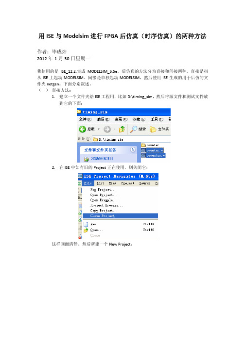
(一) 直接方法:1.建立一个文件夹给ISE工程用,比如D:\timing_sim,然后将源文件和测试文件放到它的下面:2.在ISE中如有旧的Project正在使用,则关闭它:这样画面清静。
然后新建一个New Project,点Next,选好器件和仿真器:点Next,点Finish.为了能够在ISE中直接唤起MODELSIM,还需要一些设置,主要是两处:双击器件:保证下图红圈处选中你要的仿真器:点OK后,在主菜单中点:保证在红圈处指定好MODELSIM执行文件所在的位置编译仿真库可以在这里双击Compile HDL Simulation Libraries,也可以在C:\Xilinx\12.2\ISE_DS\ISE\bin\nt下面找到,双击它,注意红圈处所标的是你的ISE版本所支持的MODELSIM版本,不能低于它。
否则仿真过程可能出问题。
点Next,点Next,选定你针对什么器件编译仿真库,点Next,点Next,注意,ISE可能最初不带modelsim.ini,它在此步会自动生成这个文件,并且是可写的,即它的“只读”属性是已经自动去掉的。
生成仿真库的映射关系自动写入了ISE的这个modelsim.ini,位于C:\Xilinx\12.2\ISE_DS\ISE\bin\nt,但是,它并不会自动去更新MODELSIM软件的modelsim.ini,而且MODELSIM使用的是它自己的modelsim.ini,位于C:\modeltech_6.5e。
所以需要把ISE的modelsim.ini中的映射关系再COPY到MODELSIM自己的modelsim.ini中。
如何在ISE环境中使用ModelSim仿真
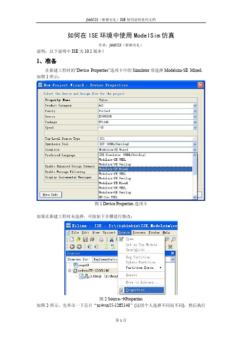
如何在ISE环境中使用ModelSim仿真作者:jbb0523(彬彬有礼)说明:以下说明中ISE为10.1版本!1、准备在新建工程时的“Device Properties”选项卡中的Simulator项选择Modelsim-SE Mixed,如图1所示:图1 Device Properties选项卡如果在新建工程时未选择,可按如下步骤进行修改:图2 Source- Properties如图2所示,先单击一下芯片“xc4vsx55-12ff1148”(这因个人选择不同而不同),然后执行Source——Properties,修改即可。
2、仿真步骤1)如图3所示,在需要仿真的源文件上右击,选择“New Source…”图3 右击---New Source2)如图4所示,在Select Source Type选项卡中选择“Verilog Test Fixture”,输入File name,单周next,直到完成。
图4 Select Source Type3)将source for选择为“Behavioral Simulation”,打开刚刚新建的文件,编辑该文件,输入仿真需要的代码(其实就是对输入信号进行配置)。
然后双击过程管理区的“Simulate Behavioral Model”,即可自动打开ModelSim进行仿真(此时ModelSim不能处于打开状态,否则会出错的),如图5所示(注意图中每一处用红线标记的部分)。
4)如果是首次仿真,ModelSim会出现如下错误:图6 ModelSim error这是一个很普遍的错误,百度此错误中的关键字“Failed to access library 'xilinxcorelib_ver' at "xilinxcorelib_ver".”即可找到解决办法。
如图7所示,Source for中重新选择Implementation,其它按照图中的红线标识单击或选择,然后双击“Compile HDL Simulation Libraries”,等待编译成功结束后,重新执行步骤3)即可。
步骤详细-ISE中使用chipscope
说明:核插入器不仅能产生常用的核,还能将其自动插入设计网表,不需要手工在HDL代码中例化,它在很多场合替代了核生成器的功能。
在ISE中直接调用ChipScope的应用实例。
在XC3S500E芯片上实现一个计数器实例,详细介绍如何在ISE中新建ChipScope应用以及观察、分析数据的操作。
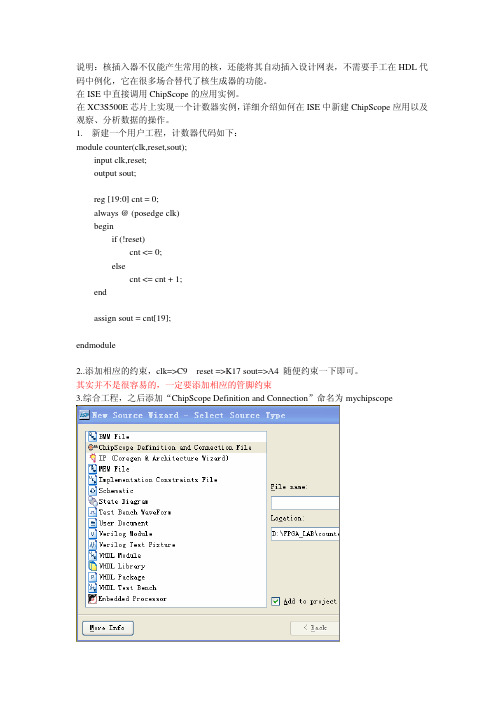
1.新建一个用户工程,计数器代码如下:module counter(clk,reset,sout);input clk,reset;output sout;reg [19:0] cnt = 0;always @ (posedge clk)beginif (!reset)cnt <= 0;elsecnt <= cnt + 1;endassign sout = cnt[19];endmodule2..添加相应的约束,clk=>C9 reset =>K17 sout=>A4 随便约束一下即可。
其实并不是很容易的,一定要添加相应的管脚约束3.综合工程,之后添加“ChipScope Definition and Connection”命名为mychipscope2.在工程区双击mychipscope.cdc文件,即可自动打开ChipScope Pro Inserter软件。
设置参数。
添加触发单元设置触发位宽。
其中触发类型选为Basic,位宽为20bit,设置采样深度为4096。
其中Number of input trigger port---用于设定触发端口数,每个端口ILA核可以支持多路比特数据,最多可有16个端口,具体的比特数取决于用于测试的逻辑资源。
Trigger Width用于设定每个端口的触发比特数。
#Match Units为触发单元的级联数,最多可设置16级,默认选择1级吧。
Sample on Rising Clock Edge--样本在时钟的上升沿进行采样。
选中Data Same As Trigger选项,则数据与触发信号相同,这是一种很常用的模式,可以捕获和采集触发逻辑分析仪的任何数据。
ISE中chipscope的使用
ChipScope Debug LabIntroductionThis lab guides you through the process of inserting ChipScope-Pro cores into your design and performing on-chip verification.ObjectivesAfter completing this lab, you will be able to:• Create a new ChipScope-Pro source in ISE• Create ILA and ICON cores using ChipScope-Pro and insert it into a PicoBlaze design • Specify trigger options in ChipScope Analyzer• Download the bitstream and run the design in hardware• Perform an on-chip verification and view the wave forms in ChipScope AnalyzerDesign DescriptionYou will extend the lab 5 design by adding a ChipScope ILA core to the PicoBlaze output bus. Next, you will setup the trigger to capture data when text is entered via Hyper Terminal. You should see the resulting text displayed in ChipScope when the buffer is full.ProcedureThis lab is separated into steps that consist of general overview statements that provide information on the detailed instructions that follow. Follow these detailed instructions to progress through the lab. This lab comprises 4 primary steps: You will create a new ChipScope source, configure and connect an ILA core, configure ChipScope Analyzer trigger options and, finally, perform an on-chip verification. Note: If you are unable to complete the lab at this time, you can download the lab files for this module from the Xilinx University Program site at /universityGeneral Flow for this LabStep 1:Creating a New ChipScope SourceStep 2: Configure and Connect an ILA Core Step 3:Configure ChipScope Analyzer Trigger OptionsStep 4: Perform an On-chip VerificationCreate a New ChipScope Source Step 1 1-1. Open a ChipScope-Pro project from lab6 folder (under vhdl or verilog).1-1-1. Open the Xilinx ISE software by selecting Start All Programs Xilinx ISE Design Suite13.2 ISE Design Tools Project Navigator.1-1-2. Open the project by selecting File Open Project.○Verilog users: Browse to c:\xup\fpgaflow\labs\verilog\lab6\chipccope○VHDL users: Browse to c:\xup\fpgaflow\labs\vhdl\lab6\chipscope1-1-3. Select chipscope.xise and click Open.1-1-4. Create a new ChipScope Definition and Connection File source by selecting Project New Source and entering the name loopback_cs. Click Next to continue.Figure 1. New Source Dialog Box1-1-5. Click Finish. A ChipScope-Pro source will be added to the Sources in Project window.Genesys 6-2 /universityFigure 2. ChipScope Definition and Connection (.cdc) added to VHDL ProjectConfigure and Connect an ILA Core Step 2 2-1. Connect the ILA core to the PicoBlaze output.2-1-1. Double-click the loopback_cs.cdc file in the sources in project window to open the core inserter project.Figure 3. ChipScope-Pro Core InserterNote: Projects saved in the Core Inserter hold all relevant information about source files, destination files, core parameters and core settings.2-1-2. Click Next and then click New ILA Unit. Notice in the left hand window how an instance of the ILA core, U0:ILA, is added to the system.Genesys 6-4 /universityFigure 4. Insert a new integrated logic analyzer (ILA) Unit2-1-3. Click Next to setup the trigger parameters.Each ILA or ILA/ATC core can have up to 16 separate trigger ports that can be setup independently. The individual trigger ports are buses that are made up of individual signals or bits that can range from 1 to 256 bits. Each trigger port can be connected to 1 to 16 match units. A match unit is a comparator that is connected to a trigger port and is used to detect events on that trigger port. The results of one or more match units are combined together to form the overall trigger condition event that is used to control the capturing of data. The different comparisons or match functions that can be performed by the trigger port match units depend on the type of match unit. The ILA and ILA/ITC cores support six types of match units. In this lab, you will setup the ILA core to trigger via some UART control signals.2-1-4. Set the following ILA trigger parameters as follows and then click Next.Trigger Input and Match Unit Settings.• Number of input trigger ports: 3Trigger Port Trigger Width # Match Units Counter WidthMatch Type TRIG0 1 1 Disabled Basic TRIG1 1 1 Disabled Basic TRIG211DisabledBasicTrigger Condition Settings• Enable Trigger Sequencer: Checked (This allows you to specify a sequence of events to enable triggering)•Max Number of Sequencer Levels: 2Storage Qualification Condition Settings• Enable Storage Qualification: Checked (This allows you to specify which data will be stored in the internal buffer)Figure 5. Specify the Trigger ParametersThe maximum number of data sample words that the ILA core can store in the sample buffer is called the data depth. The data depth determines the number of data width bits contributed by each block RAM unit used by the ILA unit. The maximum number of data sample words that can be captured depends on the number and size of block RAM, which varies according to device family and density.2-1-5. Set the following capture parameters and click Next.• Data Depth: 1024• Sample On: Rising clock edge• Data Same as Trigger Port: unchecked• Data Width: 8Figure 6. Specify Trigger ParametersThe net connections tab allows you to choose the signals to connect to the ILA core. If trigger is separate from data, then clock, trigger, and data must be specified. Connections that have not been made will appear in red.Figure 7. Unconnected Net Connections2-1-6. Click the Modify Connections tab.Figure 8. Net ConnectionsThe Select Net dialog provides an easy interface to choose nets to connect to the ILA, ILA/ATC or ATC2 cores. The hierarchical structure of the design can be traversed using the Structure/Nets pane. All the design’s nets of the selected structure hierarchy appear in the table at the lower left pane. The Clock Signals and Trigger/Data Signals tabs illustrate the net connections between the design and the ILA core.2-1-7. With the Clock Signals tab under Net Selections selected, highlight the entry for clk55MHz in the listing of nets and click the Make Connections button to connect the clock signal in the design to the clock port of the ILA core.Figure 9. Connect the clockGenesys 6-6 /university2-1-8. Click the Trigger Signals tab, and connect the three trigger ports as follows:• TP0: data_present (this signal indicates that data is present in the uart_rx module• TP1: read_from_uart (input to uart_rx that indicates that a read operation will occur)• TP2: write_to_uart (input to uart_tx that indicates that a write operation will occur)2-1-9. Click the Data Signals tab and connect the output port of the PicoBlaze controller to the data port of the ILA core (see Figure 10), and click OK.Figure 10. Connect the PicoBlaze output port2-1-10. You will notice that the Clock, Trigger, and Data ports under Net Connections are highlighted in black, indicating valid connections. Click Return to Project Navigator and save the file.Figure 11. Connection between Design and ILA core EstablishedConfigure ChipScope Analyzer Trigger Options Step 3 3-1. You will download the bitstream using ChipScope and configure the ILA core to trigger when the UART reads text from Hyper Terminal.3-1-1. With the top-level file (loopback.v/vhd) selected, double-click on Analyze Design Using ChipScope in the Processes window.3-1-2. Connect up the download cable and power up the Genesys board.3-1-3. Click the Open Cable/Search JTAG Chain button.Figure 12. Establish JTAG Connection3-1-4. Chipscope Pro Analyzer will automatically detect the devices on the Genesys board and then click OK.Figure 13. Impact Detects Devices in JTAG Chain3-1-5. Right Click on the xc5vlx50t device and select configure.3-1-6. Click Select New File and select the loopback.bit bitstream file from the project directory. Note that the import cdc file field shows the cdc file located in the project directory. Also note that the tool will create a bus (out_port) automatically. Click OK.Double-click on Trigger Setup and Waveform entries in Project Tree to open the respective windows.The ChipScope Pro Analyzer interface consists of four parts:Genesys 6-8 /universityFigure 14. ChipScope Analyzer WindowEach ChipScope Pro ILA, ILA/ATC, and IBA core has its own Trigger setup window, which provides a graphical interface for the user to setup triggers. The trigger mechanism inside each ChipScope Pro core can be modified at run-time without having to recompile the design. There are three components to the trigger mechanism:• Match Functions: Defines the match or comparison value of each match unit• Trigger Conditions: Defines the overall trigger condition based on a binary equation or sequence of one or more match functions• Capture Settings: Defines how many samples to capture, how many capture windows, and the position of the trigger in those windowsIn this design, you will setup the triggers to capture text at the PicoBlaze output port, after being entered via Hyper Terminal.3-1-7. Specify the Match Units as follows:• M0:TriggerPort0 (data_present): Value 1• M1:TriggerPort1(read_from_uart): Value 1• M2:TriggerPort1(write_to_uart): Value 1Figure 15. Setup the Match Units3-1-8. Click the field under Trigger Condition Equation, set the equation M0 M1 in the Sequencertab, and then click OK.Genesys 6-10 /universityFigure 16. Trigger Condition Equation3-1-9. Check the field next to Storage Qualification , select the AND Equation , and check M2. ClickOK . This will enable the ILA core to capture data in the buffer only when data is present, and not on every single clock edge.Figure 17. Storage Qualification EquationPerform an On-Chip VerificationStep 44-1.Start Hyper-Terminal program. Set baud rate to 9600. Arm the trigger and view the waveforms of the captured data.4-1-1.Start the Hyper-Terminal program. Make sure that the baud rate is set to 9600.Lab WorkbookChipScope Debug Lab/university Genesys 6-11xup@4-1-2. Set the buffer depth to 16.Figure 18. Select Buffer Depth4-1-3. Cick the Apply Settings and Arm Trigger button.Figure 19. Apply Settings and Arm Trigger4-1-4. Type “Xilinx #1 FPGA!” in Hyper Terminal and view the message in ChipScope Analyzer.Figure 20. Output in Waveform Window4-1-5. Close all applications without saving ChipScope project.ConclusionYou inserted the ILA and ICON cores into the PicoBlaze design, set up trigger conditions in ChipScope Analyzer, performed an on-chip verification, and analyzed the waveforms in ChipScope-Pro Analyzer.。
modelsim使用教程
modelsim使用教程ModelSim是一款常用的硬件描述语言(HDL)仿真工具,本教程将向您介绍如何使用ModelSim进行仿真。
步骤1:安装ModelSim首先,您需要下载和安装ModelSim软件。
在您的电脑上找到安装程序并按照提示进行安装。
步骤2:创建工程打开ModelSim软件,点击"File"菜单中的"New",然后选择"Project"。
在弹出的对话框中,选择工程的存储位置,并为工程命名。
点击"OK"完成工程创建。
步骤3:添加设计文件在ModelSim的工程窗口中,右键点击"Design"文件夹,选择"Add Existing File"。
然后选择包含您的设计文件的目录,并将其添加到工程中。
步骤4:配置仿真设置在工程窗口中,右键点击"Design"文件夹,选择"Properties"。
在弹出的对话框中,选择"Simulation"选项卡。
在"Top level entity"字段中,选择您的设计的顶层模块。
点击"Apply"和"OK"保存设置。
步骤5:运行仿真在ModelSim的工具栏中,找到"Simulate"按钮,点击并选择"Start Simulation"。
这将打开仿真窗口。
在仿真窗口中,您可以使用不同的命令来控制和观察设计的行为。
步骤6:查看仿真结果您可以在仿真窗口中查看信号波形、调试设计并分析仿真结果。
在仿真窗口的菜单栏中,您可以找到一些常用的查看和分析工具,如波形浏览器、信号分析器等。
步骤7:结束仿真当您完成仿真时,可以选择在仿真窗口的菜单栏中找到"Simulate"按钮,并选择"End Simulation"以结束仿真。
modelsim使用技巧

modelsim使用技巧ModelSim是一款常用的仿真工具,用于学习、开发和测试各种数字电路和系统设计。
它提供了大量的功能,可以帮助我们更好地进行仿真、调试和性能优化。
但是,对于初学者来说,熟练使用ModelSim可能需要一些时间和实践。
在本文中,我们将介绍一些ModelSim的使用技巧,以帮助读者更好地掌握这个工具。
一、基本操作1.创建工程在ModelSim中,创建工程是第一步。
可以通过File -> New -> Project来创建一个新的工程。
在工程创建过程中,需要指定工作目录、项目名称和工具链等信息。
在创建工程后,可以右键单击仿真文件夹,并选择添加到工程来添加设计文件。
2.添加仿真文件在ModelSim中,添加仿真文件非常简单。
可以将文件拖放到仿真文件夹、使用File -> Add to Project选项或使用命令行方式添加文件。
一旦添加了仿真文件,可以使用filelist命令查看所有添加的文件。
3.编译设计在ModelSim中,编译由两个阶段组成。
第一阶段称为分析阶段,在此阶段中,设计的各个模块被分析、组合并建立数据结构。
第二阶段称为综合阶段,在此阶段中,数据结构被综合成一个整体,并生成仿真网表。
可以通过compile option来指定编译选项,比如-v库等。
4.运行仿真在ModelSim中,可以通过三种方式来运行仿真。
第一种是在命令行中使用run命令,第二种是通过菜单和工具栏选项来启动仿真,第三种是使用脚本方式启动仿真。
在仿真过程中,可以使用wave、add wave、force、release等命令来控制信号的行为。
二、ModelSim高级技巧1.波形窗口波形窗口是ModelSim中最有用的窗口之一。
可以使用Add Wave按钮打开该窗口。
在波形窗口中,可以查看所有信号的变化情况。
可以使用full view、zoom in、zoom out等选项来放大或缩小波形窗口。
modelism简明操作指南

第一章介绍ModelSim的简要使用方法第一课 Create a Project1.第一次打开ModelSim会出现Welcome to ModelSim对话框,选取Create a Project,或者选取File\New\Project,然后会打开Create Project对话框。
2.在Create Project对话框中,填写test作为Project Name;选取路径Project Location作为Project文件的存储目录;保留Default Library Name设置为work。
3.选取OK,会看到工作区出现Project and Library Tab。
4.下一步是添加包含设计单元的文件,在工作区的Project page中,点击鼠标右键,选取Add File to Project。
5.在这次练习中我们加两个文件,点击Add File to Project对话框中的Browse 按钮,打开ModelSim安装路径中的example目录,选取counter.v和tcounter.v,再选取Reference from current location,然后点击OK。
6.在工作区的Project page中,单击右键,选取Compile All。
7.两个文件编译了,鼠标点击Library Tab栏,将会看到两个编译了的设计单元列了出来。
看不到就要把Library的工作域设为work。
8.最后一不是导入一个设计单元,双击Library Tab中的counter,将会出现Sim Tab,其中显示了counter设计单元的结构。
也可以Design\Load design 来导入设计。
到这一步通常就开始运行仿真和分析,以及调试设计,不过这些工作在以后的课程中来完成。
结束仿真选取Design \ End Simulation,结束Project选取File \ Close \ Project。
ISE软件使用说明
ISE软件使用说明ISE(Integrated Software Environment)软件是由赛灵思公司(Xilinx Inc.)开发的一款用于设计和开发数字电路的软件工具。
该软件提供了一个集成的环境,用于设计、模拟和验证数字电路。
本文将介绍ISE软件的安装和基本使用方法,以帮助用户快速上手。
一、安装ISE软件2.根据安装程序的提示,选择安装的目标文件夹和所需的组件。
3.等待安装程序完成安装。
二、打开ISE软件打开ISE软件后,会出现一个欢迎界面,用户可以选择新建项目、打开已有项目或者直接进入ISE工具链。
三、创建新项目1. 点击“New Project”按钮,进入新项目设置页面。
2.输入项目的名称和路径,选择项目类型和芯片系列。
3. 点击“Next”按钮,进入项目配置页面。
4.在此页面中,用户可以添加需要使用的源文件、约束文件和IP核等。
5. 点击“Next”按钮,进入总结页面。
6. 点击“Finish”按钮,完成项目创建。
四、设计源文件在ISE软件中,用户可以使用HDL(硬件描述语言)进行设计源文件的编写。
ISE软件支持的HDL语言有VHDL和Verilog。
1. 在项目视图中,右键点击“Source”文件夹,选择“New Source”。
2.在弹出的对话框中,选择源文件类型和语言。
3. 输入文件的名称和路径,点击“Finish”按钮。
五、添加约束文件约束文件用于定义电路的时序、引脚映射等信息,以确保电路的正常工作。
1. 在项目视图中,右键点击“Constraints”文件夹,选择“New Source”。
2.在弹出的对话框中,选择约束文件类型。
3. 输入文件的名称和路径,点击“Finish”按钮。
六、综合与实现在进行综合和实现之前,需要根据设计需求进行一些设置和配置。
1. 在项目视图中,右键点击项目名称,选择“Properties”。
2.在弹出的对话框中,选择“SYNTHESIS”或“IMPLEMENTATION”选项卡。