最新开关电源设计及其英文翻译
开关电源发展轨迹中英文翻译资料

Switching Power Supply Development TrackDevelopment of switching power supply (Review Xuanlan) switching power supply (hereinafter referred to switch power) to replace the linear regulator power transistors (hereinafter referred to the linear power) has 30 years of history, is the earliest the series switching power supply, its main Linear power supply topologies and similar, but the power transistor to switch to a later state PWM (PWM) control techniques have been developed for the control switch converters, by PWM switching power supply, it is characterized by using 20 kHz frequency or pulse PWM a PWM switching power supply efficiency is about 65 to 70 percent, while the efficiency of linear power only 30 of a 40 per cent. In the event of the world's energy crisis, caused people to a wide range of customs. Linear power supply works in the frequency, the frequency used for the 20 kHZ the PWM switching power supply alternatives, could significantly conserve energy and power technology in the history of the development called 20 kHZ revolution. With ULSI chip size decreases, the size and power is much greater than the microprocessor; spacecraft, submarines, military power and switch the batteries used portable electronic devices (such as mobile computers, mobile phones, etc.) need more small , Lightweight power. Hence the switch to power a small light requirements, including magnetic components and capacitors the size of small weight. In addition switching power supply requirements to higher efficiency, better performance, reliability, and so on. China's switching power supply from China's history of the development process of switching power supply can understand the international development of a switching power supply side, although generally speaking, China's level of technological development with the international advanced level in an average of 5 to 10 gap. 1970s, I join in black and white TV sets, small and medium-sized computer in the beginning of 5 V ,20-200A, 20kHZ AC-DC switching power supply. 1980s into mass production and extensive application stage and Development of 0.5 ~ 5 MHz quasi-resonant soft-switching power supply. In the 1980s, China's communications (such as the switch-Note) in the AC-DC power supply and DC-DC switching power supply in the area of application is still relatively low proportion of six. The end of the 1980s large-scale upgrading of China's communication power, the traditional ferromagnetic regulator - Rectifier and SCR (Thyristor, formerly known as SCR components) Phased power supply for high-power (48 V, 6kw) AC-DC Switching Power Supply (often referred to as communications systems switch Rectifier SMR) by substituting, and started in the office automation equipment in the applications. Industrial applications, in the boiler flame control, protection, laser, color TV, the filament-emission current regulation, ion-injection machine, Luwu Deng control systems in both applications. The 1990s, China's also developed a number of new non-clearance for power, the typical examples are as follows: 1. Satellite switching power supply. The East is Red on the 3rd communication satellite, Fengyun 1, 2 meteorological satellite applications are the switching power supply. Features: Multi-output, non-maintenance, long-term requirements do not change the performance, set up redundant modules, high reliability, EMC meet the space environment conditions, high efficiency, small light. 2 long-range rocket control system for DC-DC switching power supply to launch the process of highly reliable. 3 1000kW traction converter 4500 V/1200A GTO gated 250 W switching power supply. 4 40kW solid pulse laser soft switching power supply. 10 kw with four more resonant full bridge ZVS converters parallel. 5. Welder double-IGBT forward to the voltage conversion for a pulse modulation (ZVT-PWM) soft switching power supply. Output 20 kW, 500A, switching frequency of 40 kHZ, the efficiency of 92%. Is characterized by frequent changes in the scope of the load, poor working environment. Impact on the current power demand, dynamic characteristics, and no overshoot, load affecting soft-switch nature. 6. Substation in the current operating system switching power supply. For the protection and automatic devices and battery charging. Surge instead of SCR system, the output 10 A, 180 ~ 286V. Main switch IGBT or effective power MOSFET. 7. Single-phase and three-phase rectifier high power factor (with the number of active power correction). One can see that20 of 30, China's switching power supply applications and technical performance of great progress, and the family foundation is closely related to industry and enhance the national strength, and international advanced technology affecting the power switch. China fully demonstrated the power of talent and technical personnel of the entrepreneurial spirit of arduous struggle. In the 1990s, small and medium-sized (500 W below) AC-DC and DC-DC switching power supply is characterized by: high frequency of (switching frequency of 300-400 kHZ) to achieve high power density, a small amount of light; to efficient and reliable; Low-cost, low output voltage (≤3 V; AC input with a few high-power, etc. In the next five years will continue along these directions. Main technical marks from a technical perspective, for several decades to promote switching power supply performance and constantly improve the technological level This should mark is: 1. A new high-frequency power semiconductor devices to achieve the development of high-frequency switching power supply may have. IGBT such as power MOSFET and has been fully replace the power transistor and SCR, so that small and medium-sized switch power下作Frequency of up to 400 kHZ (AC-DC) and 1 MHZ (DC-DC) level. Ultrafast restore power diode, MOSF ET asked further rectification technology for the development of efficient low-voltage output (for example, 3 V) switching power supply for a possible . Are now exploring the development of high-performance high temperature carbonation power to block conductor devices 2. Soft-switch technology enables efficient high-frequency converter with the realization may be. PWM switching power supply switch-mode by hard work (on / off process BU voltage drop / rise and the current rise / fall waveform is overlap), thus the switching losses. High-frequency switching power supply can reduce the volume of weight, but switching losses are greater (power and frequency is directly proportional). So we must Switching on power than / current wave of cross more technology, the so-called zero-voltage (ZVS) / the current (ZCS) switching technology, or soft-switch technology (as opposed to PWM switching technology in terms of hardware), the small soft-switching power supply efficiency Can be increased to 80 a 85 per cent. 1970s, switching power supply market was soft-switch technology laid the foundation. After the new soft-switch technology will continue to emerge, such as the quasi-resonant (1980s) full-bridge phase-shift ZVS-PWM, constant frequency ZVS -PWM/ZCS-PWM (80 in the late) ZVS-PWM active clamp; ZVT-PWM/ZCT-PWM (90 in the early) full-bridge phase-shift ZV-ZCS-PWM (90 years), and so on. China has The latest soft-switching technology to 6 Kw power of communication, efficiency up to 93% 3. Control Technology progress. Such as the current control and multi-loop control, load control, a cycle control, power factor control, DSP control, and the corresponding private Integrated control of the successful development of the chip, so that switching power supply has greatly improved dynamic performance, the circuit also greatly simplified 4. Active Power Mission of Correction (APFC) the development, improve the AC-DC switching power supply power factor. Due to the importation Rectification of a capacitor-a device, AC-DC switching power supply and a large class of the rectifier power supply electronic equipment (such as inverters, UPS), and so the power grid measuring only a few corporations with the APFC 0.65,80 technology can improve To 0.95 to 0.99, both the management of the power grid harmonic "pollution" and also improve the overall efficiency of the power switch. APFC is a single-phase DC-DC converter topology and power factor control of specific applications, while the three-phase APFC Three-Phase PWM switch is rectifier topology and control technology with 5. Magnetic components of new magnetic materials and the development of a new transformer. Such as integrated magnetic circuit, the plane Cores, ultra-thin (Low profile) transformer and a new transformer such as piezoelectric , No Cores printed circuit (PCB) transformer, so that the power switch can reduce the size of the weight of many 6. Capacitors and EMI filter new advances in technology, so that small switching power supply and improve the performance of EMC 7. Micro-processing For monitoring and switching power supply system of internal communication technology applications, improve the reliability of the power system. The late 1990s and made a newswitching power supply of research and development, this is also the new century vision for the development of switching power supply. Such as: an AC - DC converter or regulator to achieve steady flow, and a power factor correction feature, known as single-level (SingleSwitch Single Stage) or 4 S high power factor AC-DC converter output 1 V, 50A of the low-voltage high-current DC-DC converters, also known as voltage regulator module VRM, to adapt to the next generation of ultra-fast microprocessor power supply needs of multi-channel (Multi-Channel or Multi-Phase) DC-DC converter; web server (Server) The switching power supply to be a portable electronic equipment such as the high-frequency switching power supply. More than a brief review of the process of switching power supply development and the performance. I believe the 21st century, the power switch theory and technology development will have a more brilliant achievements , I hope this message of the cross-century youth power experts.开关电源发展轨迹开关电源发展轨迹(察宣兰)开关稳压电源(以下简称开关电源)取代晶体管线性稳压电源(以下简称线性电源)已有30多年历史,最早出现的是串联型开关电源,其主电路拓扑与线性电源相仿,但功率晶体管了作于开关状态后来脉宽调制(PWM)控制技术有了发展,用以控制开关变换器,得到PWM开关电源,它的特点是用20kHz脉冲频率或脉冲宽度调制一PWM开关电源效率可达65~70%,而线性电源的效率只有30一40%。
毕业设计论文 外文文献翻译 基于PLC双电源开关设计外文翻译 中英文对照

毕业设计论文外文文献翻译基于PLC双电源开关设计外文翻译中英文对照英文题目 Based on PLC dual power switch design 中文题目基于PLC双电源开关设计系 (院) 自动化系专业电气自动化技术滨州学院专科毕业设计(外文翻译)Intelligent double power1 Intelligent dual power supply switching technologyIn this paper, the double load - dual power automatic switching of PLC control, PLC control program to replace relay logic control circuits, it has the three-phase power supply phase detection and protection switching function, power returned to normal after the automatic reverse switch, when a fault and restore normal respectively sends out two difference clear alarm and prompt sound. Double load - dual power automatic switching control of PLC, the open-phase protection mainly adopts the technical proposal that : setting the three-phase open-phase detection signal circuit, the three-phase open-phase detection signal circuit directly from the main circuit of three-phase power supply, namely the intermediate relay KA1-KA3 and KA4-KA6, respectively connected to power supply main loop U1 and U2 A, B and C single phase circuit, KA1-KA3 and KA4-KA6 normally open contacts respectively as PLCinput signal, namely as the preparation of PLC U1 and U2 three-phase open-phase detection logic control program input conditions. With short phase protection double load - dual power automatic switching control, not only has the open-phase protection, but also has a short circuit and overload protection, under-voltage protection function; automatic phase lack detection, three-phase current display, a road power supply circuit can automatically switch to another power source to load power supply, light and sound alarm; in the power supply return to normal after automatic reverse switch; in the event of a failure and return to normal when respectively sends out two difference obvious alarm and prompt sound effects. It overcomes the shortcomings of low double power supply switching control system without phase protection, can automatically reverse switch, as well as fault and return to normal when using asingle audio prompts defects. The control system has perfect function, reliable performance, simple circuit structure, low manufacturing cost etc...2 Intelligent dual power supplies switching main circuit controlWith short phase protection double load - dual power automatic switching control circuit. It includes a main circuit and three-phase short signal detecting sampling circuit. The main circuit of the input power supply power supply U1 and U2, its output has two2滨州学院专科毕业设计(外文翻译)loads W1 and W2. Power main circuit of AC contactor U1 through KM1 main contacts and a load of W1 connected; power supply U2 main circuit through the AC contactor KM2 main contacts and a load of W2 connected; under the control of a control circuit, a power failure occurs, the AC contactor lost the first electrically disconnected, so that the load of detachment faults power supply circuit, the AC contactor KM3 main contact closing conduction contact loop, will be connected to the fault loop load switch automatically to another normal power supply continues to supply. Power supply U1 and U2 main circuit input end of the automatic switch in QF1 and QF2 is the primary role of overload protection and short-circuit protection; two phase power supply main loop in each phase are current meter to indicate the phase current status, with the control circuit of phase lack detection. The three-phase open-phase detection signal sampling circuit, the phase detection signal directly from the main circuit of three-phase power supply, namely the intermediate relay KA1 ~ KA3KA4 ~ KA6 are respectively connected to the power supply main loop U1 and U2 A, B phase and C phase of the single-phase circuit, KA1 ~ KA3 and KA4 ~ KA6 normally open contact as U1 and U2 three-phase open-phase detection switch sampling signal, to the PLC input terminal. Considering the PLC relay output point load capacity, through the contactor KM01 ~ KM03 to drive high current contactor KM1 ~ KM3.For three-phase power U1 A, B phase and C phase lack detection, the use of an intermediate relay KA1, KA2 and KA3, respectively connected topower the U1 main circuit A, B phase and C phase and zero line N constitute a single-phase circuit, the formation of A1, B1 and C1 phase detection circuit. The normally open contact of KA1 ~ KA3 as U1 three-phase.Phase lack detection switch sampling signal, to the PLC input terminal, used in the preparation of PLC U1 three-phase open-phase detection logic control program input conditions; similarly, the three-phase power supply U2 A, B phase and C phase lack detection, but also the use of an intermediate relay KA4, KA5 and KA6, respectively connected to power the U2 main circuit A2, B2 phase and C2 phase and zero line N constitute a single-phase circuit, the formation of A2, B2 and C2 three-phase open-phase detection circuit. KA4 ~ KA6 normally open contacts respectively as U2 three-phase open-phase detection switch sampling signal, to the PLC input terminal, used in the3滨州学院专科毕业设计(外文翻译)preparation of PLC U2 three-phase open-phase detection logic control program input conditions.3 With PLC intelligent dual power controlThe three-phase open-phase detection signal sampling circuit, as U1 and U2 three-phase open-phase detection switch sampling signals of KA1-KA3 and KA4-KA6, the normally open contacts respectively for the input of the PLC X0-X2, X3-X5. In the PLC ladder diagram program, auxiliary relay R1 as the three-phase power supply of U1 three-phase open-phasedetection, which is normally open input conditions for X0, X1 and X2" and" logic; similarly, internal intermediate relay R2 as the three-phase power supply of U2 three-phase open-phase detection, it’s on conditions for the normally open input X3, X4 and X5" and" logic.In automatic switching control process, PLC ladder diagram procedure of auxiliary relay R1 and R2 respectively controlled AC contactor KM1 ( Y0 ) and KM2 ( Y1 ) coil and electric state, directly reflects two three-phase power supply U1 and U2 respectively the total phase condition, namely, either U1 or U2 three-phase power supply phase, KM1 ( Y0 ) or KM2 ( Y1 ) will immediately loses electricity, the normally closed contact of the alternating current contactor closed KM3 ( Y2 ) control coil gets electricity to attract, through the KM3 main contacts closed conduction contact loop, will be connected to the fault circuit load W1 or W2 automatically switches to a normal power supply U2 or U1 to power supply, so as to realize open-phase protection automatic switching. In automatic switching control process, auxiliary relay R1 and R2 main function is: when troubleshooting, three-phase power U1 orU2 recover the normal power supply, R1 (or R2) have electricity, the normally closed contact action, R3 reset, cut KM3 (Y2), then KM1 (Y0) or KM1 (Y1) complex have electricity, thereby automatically reverse switching back to the power supply to load W1 U1, U2 W2 power supply to load the normal power supply state.The control circuit adopts electric whistle (or buzzer) as an alarm sound (at) the same time with the red signal (at the same time with thered signal lamp), and returned to normal when the bell HA as prompt sound. Can produce two distinct alarms and prompt sound effects.4滨州学院专科毕业设计(外文翻译)智能双电源1 智能双电源切换的技术方案本文所述的双负载—双电源自动切换的PLC控制,用PLC控制程序取代继电器逻辑控制电路,其具有对三相供电电源的缺相检测及保护切换功能,在电源恢复正常后能自动进行反切换,当发生故障和恢复正常时能分别发出两种区别明显的报警和提双负载—双电源自动切换的PLC控制,其缺相保护主要采取的技术方案是:示音响。
史上最全的开关电源专业英语词汇
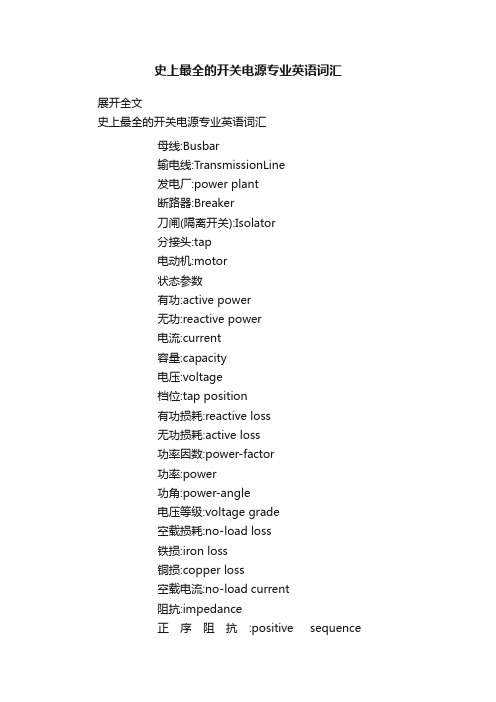
史上最全的开关电源专业英语词汇展开全文史上最全的开关电源专业英语词汇母线:Busbar输电线:TransmissionLine发电厂:power plant断路器:Breaker刀闸(隔离开关):Isolator分接头:tap电动机:motor状态参数有功:active power无功:reactive power电流:current容量:capacity电压:voltage档位:tap position有功损耗:reactive loss无功损耗:active loss功率因数:power-factor功率:power功角:power-angle电压等级:voltage grade空载损耗:no-load loss铁损:iron loss铜损:copper loss空载电流:no-load current阻抗:impedance正序阻抗:positive sequenceimpedance负序阻抗:negative sequence impedance零序阻抗:zero sequence impedance电阻:resistor电抗:reactance电导:conductance电纳:susceptance无功负载:reactive load 或者QLoad有功负载: active load PLoad遥测:YC(telemetering)遥信:YX励磁电流(转子电流):magnetizing current定子:stator功角:power-angle上限:upper limit下限:lower limit并列的:apposable高压: high voltage低压:low voltage中压:middle voltage电力系统 power system发电机 generator励磁 excitation励磁器 excitor电压 voltage电流 current母线 bus变压器 transformer升压变压器 step-up transformer高压侧 high side输电系统 power transmission system输电线 transmission line固定串联电容补偿fixed series capacitor compensation稳定 stability电压稳定 voltage stability功角稳定 angle stability暂态稳定 transient stability电厂 power plant能量输送 power transfer交流 AC装机容量 installed capacity电网 power system落点 drop point开关站 switch station双回同杆并架double-circuit lines on the same tower变电站 transformer substation补偿度 degree of compensation高抗 high voltage shunt reactor无功补偿reactive power compensation故障 fault调节 regulation裕度 magin三相故障 three phase fault故障切除时间 fault clearing time极限切除时间 critical clearing time切机 generator triping高顶值 high limited value强行励磁 reinforced excitation线路补偿器LDC(line drop compensation)机端 generator terminal静态 static (state)动态 dynamic (state)单机无穷大系统 one machine - infinity bus system机端电压控制 AVR电抗 reactance电阻 resistance功角 power angle有功(功率) active power无功(功率) reactive power功率因数 power factor无功电流 reactive current下降特性 droop characteristics斜率 slope额定 rating变比 ratio参考值 reference value电压互感器 PT分接头 tap下降率 droop rate仿真分析 simulation analysis传递函数 transfer function框图 block diagram受端 receive-side裕度 margin同步 synchronization失去同步 loss of synchronization 阻尼 damping摇摆 swing保护断路器 circuit breaker电阻:resistance电抗:reactance阻抗:impedance电导:conductance电纳:susceptance导纳:admittance电感:inductance电容: capacitance电源英语词汇(三)coupling 耦合intermittent 周期的dislocation 错位propeller 螺旋桨switchgear 配电装置dispersion 差量flange 法兰盘dielectric 介电的binder 胶合剂alignment 定位elastomer 合成橡胶corollary 必然的结果rabbet 插槽vent 通风孔subtle 敏感的gearbox 变速箱plate 电镀crucial 决定性的flexible 柔性的technics 工艺ultimate 最终的resilience 弹性vendor 自动售货机partition 分类rigid 刚性的prototype 样机diagram 特性曲线interfere 干涉compatible 兼容的simulation 模拟clutch 离合器refinement 精加工fixture 夹具torque 扭矩responsive 敏感的tensile 拉伸cushion 减震器rib 肋strength 强度packing 包装metallized 金属化stress 应力mitigate 减轻trade off 折衷方案yield 屈伸line shaft 中间轴matrix 母体inherent 固有的spindle 主轴aperture 孔径conformance 适应性axle 心轴turbulence 扰动specification 规范semipermanent 半永久性的enclosure 机壳specialization 规范化bolt 螺栓oscillation 振幅calling 职业nut 螺母anneal 退火vitalize 激发screw 螺丝polymer 聚合体revelation 揭示fastner 紧固件bind 凝固dissemination 分发rivit 铆钉mount 支架booster 推进器hub 轴套distortion 变形contractual 契约的coaxial 同心的module 模块verdict 裁决crank 曲柄slide 滑块malfunction 故障inertia 惰性medium 介质allegedly 假定active 活性的dissipation 损耗controversy 辩论lubrication 润滑assembly 总装dictate 支配graphite 石墨encapsulate 封装incumbent 义不容辞的derivative 派生物adhesive 粘合剂validation 使生效contaminate 沾染turbine 涡轮procurement 收购asperity 粗糙bearing 支撑架mortality 失败率metalworking 金属加工isostatic 均衡的shed light on 阐明viscous 粘稠的osculate 接触adversely 有害的grinding 研磨imperative 强制的consistency 连续性corrosin 侵蚀lattice 晶格fitness 适应性flush 冲洗fracture 断裂warrant 保证inhibitor 防腐剂diffusivity 扩散率turning 车工dispersant 分散剂vice versa 反之亦然ways 导轨deteriorate 降低tribological 摩擦的hybrid 混合物neutralize 平衡screen 屏蔽ID=inside diameterpulley 滑轮exclusion 隔绝OD=outside diameter hydraulic 液压的insulation 绝缘reciprocate 往复运动delicate 精密的elaborate 加工dress 精整dampen 阻尼incontrovertible 无可争议的by and large 大体上pivotal 中枢的luminous 发光的plastic 塑胶utilitarian 功利主义out of round 失园organic 有机的grass root 基层premature 过早的film 薄膜state-of-the -art 技术发展水平guard 防护罩polyester 聚酯blade 托板permeate 渗入epoxy 环氧的carrier 载体spillage 溢出polypropylene 聚丙烯chuck 卡盘erosion 浸蚀photoconductive 光敏的infeed 横向进给routine 程序miniaturization 小型化lapping 抛光postprocess 后置处理asynchronism 异步milling 洗削solder-bump 焊点synchronization 同步speciality 专业grid 栅格respond 响应stroke 行程impedance 阻抗feedback 反馈attachment 备件approximately 大约aberrance 畸变tapered 楔形的purported 据说steady 稳态的casting 铸件consumable 消费品dynamic 动态的index 换档inductance 电感transient 瞬态的stop 挡块capacitance 电容coordinate 坐标contour 轮廓resistance 电容curve 曲线machine center 加工中心audion 三极管diagram 特性曲线capitalize 投资diode 二极管history 关系曲线potentiometer 电位器transistor 晶体管gradient 斜率know-how 实践知识choker 扼流圈parabola 抛物线potted 封装的filter 滤波器root 根mechatronics 机电一体化transformer 变压器eigenvalue 特征值stem from 起源于fuse 保险丝function 函数rule-based 基于规则的annular core 磁环vector 向量consolidation 巩固radiator 散热器reciprocal 倒数energize 激发regulator 稳压器virtual value 有效值synchronous 同时发生bobbin 骨架square root 平方根socket 插孔tape 胶带cube 立方polarity 极性ceramic capacitor 瓷片电容integral 积分armature 电枢electrolytic C 电解电容differential 微分installment 分期付款self-tapping screw 自攻螺丝hisgram 直方图lobe 凸起footprint 封装ratio 比率plunge 钻入resin 松香grade down 成比例降低servo 伺服机构solderability 可焊性proportion 比例dedicated 专用的shock 机械冲击inverse ratio 反比interpolation 插补endurance 耐久性direct ratio 正比compensation 校正initial value 初始值plus 加upload 加载flashing 飞弧subtract 减overload 过载canned 千篇一律的multiply 乘lightload 轻载lot 抽签divide 除stagger 交错排列parallel 并联impedance 阻抗traverse 横向in series 串联damp 阻尼longitudinal 纵向的equivalent 等效的reactance 电抗latitudinal 横向的terminal 终端admittance 导纳restrain 约束creep 蠕动susceptance 电纳square 平方Hyperlink 超级连接spring 触发memo 备忘录wastage 损耗presentation 陈述principle 原理binder 打包planer 刨床source program 源程序Client-Server Model客户机server 服务器table 表query 查询form 表单report 报表macro 宏module 模块field 字段record 记录。
开关电源设计及其英文翻译

Switching Power Supply DesignSwitching power supply work in high frequency, high pulse state, are analog circuits in a rather special kind. Cloth boards to follow the principle of high-frequency circuit wiring.1, layout:Pulse voltage connection as short as possible, including input switch connected to the transformer, output transformer to the rectifier tube cable. Pulse current loop as small as possible such as the input filter capacitor is returned to the transformer to the switch capacitor negative. Some out-ended output transformers are the output rectifier to the output capacitor back to transformer circuit X capacitor as close as possible to the input switching power supply, input lines should be avoided in parallel with other circuits, should be avoided. Y capacitor should be placed in the chassis ground terminal or FG connectors. A total of touch induction and transformer to maintain a certain distance in order to avoid magnetic coupling. Such as poor handling of feeling in between inductor and transformer plus a shield, over a number of EMC performance for power supply to the greater impact.General the output capacitor can be used the other two a close rectifier output terminal should be close to, can affect the power supply output ripple index, two small capacitor in parallel results should be better than using a large capacitor. Heating devices to maintain a certain distance, and electrolytic capacitors to extend machine life, electrolytic capacitors is the switching power supply bottleneck life, such as transformers, power control, high power resistors and electrolytic to maintain the distance required between the electrolyte leaving space for heat dissipation , conditions permitting, may be placed in the inlet.Control part to pay attention to: Weak signal high impedance circuit connected to sample the feedback loop as short as in the processing as far as possible avoid interference, the current sampling signal circuits, in particular the current control circuit, easy to deal with some unexpected bad The accident, which had some skill, now to 3843 the circuit example shown in Figure (1) Figure 1 better than Yu Figure 2, Figure 2 Zai full time by observing the current waveform oscilloscope Mingxian superimposed spikes, Youyuganrao limited flow ratio design Zhi Dian low, Figure 1 there is no such phenomenon, there are switch drive signal circuit, switch resistance should be close to the switch driver can switch the work to improve the reliability of this and the high DC impedance voltage power MOSFET driver characteristics.Second, routingAlignment of current density: now the majority of electronic circuit board using insulated copper constitute tied. Common PCB copper thickness of 35μm, the alignment valuecan be obtained in accordance with 1A/mm experience the value of current density, the specific calculations can be found in textbooks. To ensure the alignment principles of mechanical strength should be greater than or equal to the width of 0.3mm (other non-power supply circuit board may be smaller minimum line width). PCB copper thickness of 70μm is also common in switching power supply, then the current density can be higher.Add that, now Changyong circuit board design tool design software generally items such as line width, line spacing, hole size and so dry plate Guo Jin Xing parameters can be set. In the design of circuit boards, design software automatically in accordance with the specifications, can save time, reduce some of the workload and reduce the error rate.Generally higher on the reliability of lines or line density wiring can be used double panel. Characterized by moderate cost, high reliability, to meet most applications.The ranks of some of the power module products are also used plywood, mainly to facilitate integration of power devices such as transformer inductance to optimize wiring, cooling and other power tube. Good consistency with the craft beautiful, transformer cooling good advantage, but its disadvantage is high cost, poor flexibility, only suitable for industrial mass production.Single-sided, the market circulation of almost universal switching power supply using single-sided circuit board, which has the advantage of lower costs in the design and production technology are also taken some measures to ensure its performance.Single PCB design today to talk about some experience, as a single panel with low cost, easy-to-manufacture features, the switching power supply circuit has been widely used, because of its side tied only copper, the device's electrical connections, mechanical fixation should rely on the copper layer, the processing must be careful.To ensure good performance of the mechanical structure welding, single-sided pad should be slightly larger to ensure that the copper and substrate tied good focus, and thus will not be shocked when the copper strip, broken off. General welding ring width should be greater than 0.3mm. Pad diameter should be slightly larger than the diameter of the device pins, but not too large, to ensure pin and pad by the solder connection between the shortest distance, plate hole size should not hinder the normal conditions for the degree of investigation, the pad diameter is generally greater than pin diameter 0.1-0.2mm. Multi-pin device to ensure a smooth investigation documents can also be larger.Electrical connection should be as wide as possible, in principle, should be larger than the width of pad diameter, special circumstances should be connected in line with the need to widen the intersection pad (commonly known as Generation tears), to avoid breaking certain conditions, line and pad. Principle of minimum line width should be greater than 0.5mm.Single-board components to be close to the circuit board. Need overhead cooling device to device and circuit board between the pins plus casing, can play a supporting deviceand increase the dual role of insulation to minimize or avoid external shocks on the pad and the pin junction impact and enhance the firmness of welding. Circuit board supporting the weight of large parts can increase the connection point, can enhance joint strength between the circuit board, such as transformers, power device heat sink.Single-sided welding pins without affecting the surface and the shell spacing of the prior conditions, it can be to stay longer, the advantage of increased strength of welded parts, increase weld area and immediately found a Weld phenomenon. Shear pin long legs, the welding force smaller parts. In T aiwan, the Japanese often use the device pins in the welding area and the circuit board was bent 45 degrees, and then welding process, its reasoning Ibid. Double panel today to talk about the design of some of the issues, in relatively high number of requests, or take the line density of the larger application environments using double-sided PCB, its performance and various indicators of a lot better than a single panel.Two-panel pad as holes have been high intensity metal processing, welding ring smaller than a single panel, the pad hole diameter slightly larger in diameter than pins, as in the welding process solder solution conducive to penetrate through the top hole solder pad to increase the welding reliability. But there is a disadvantage if the hole is too large, wave soldering tin when the jet impact in the lower part of the device may go up, have some flaws.High current handling of alignment, line width in accordance with pre-quote processing, such as the width is not enough to go online in general can be used to increase the thickness of tin plating solution, the method has a good variety of1. Will take the line set to pad property, so that when the circuit board manufacturing solder alignment will not be covered, the whole hot air normally be tin plated.2. In the wiring by placing pads, the pad is set to take in line shape, pay attention to the pad holes set to zero.3. In the solder layer placed on line, this method is the most flexible, but not all PCB manufacturers will understand your intentions, needed captions. Place the line in the solder layer of the site will not coated solder tinning line several methods as above, to note that, if the alignment of a very wide all plated with tin in solder after the solder will bond a lot and distribution is very uneven, affecting appearance. Article tin can be used generally slender width in the 1 ~ 1.5mm, length can be determined according to lines, tin part of the interval 0.5 ~ 1mmDouble-sided circuit board for the layout, the alignment provides a very selective, make wiring more reasonable. On the ground, the power ground and signal ground must be separated, the two to converge in filter capacitors, in order to avoid a large pulsed current through the signal ground connection instability caused by unexpected factors, the signal control circuit grounding point as far as possible, a skill, as far as possible the alignment of the non-grounded wiring layer in the same place, the last shop in another layer of earth.Output line through the filter capacitors, the general first, and then to the load, input line must also pass capacitor, to the transformer, the theoretical basis is to ripple through trip filter capacitor.Voltage feedback sampling, in order to avoid high current through the alignment of the feedback voltage on the sampling point must be the most peripheral power output to increase the load effect of target machine.Alignment change from a wiring layer to another wiring layer generally used hole connected, not through the pin pad device to achieve, because the plug in the device may be damaged when the relationship between this connection, there is current in every passage of 1A, at least two through-hole, through hole diameter is greater than the principle of 0.5mm, 0.8mm generally processed ensure reliability.Cooling devices, in some small power supply, the circuit board traces can be and cooling, characterized by the alignment as generous as possible to increase the cooling area is not coated solder, conditions can even be placed over holes, enhanced thermal conductivity .Today to talk about the aluminum plate in the switching power supply application and multilayer printed circuit in the switching power supply applications.Aluminum plate by its own structure, has the following characteristics: very good thermal conductivity, single Mianfu copper, the device can only be placed in tied copper surface, can not open electrical connection hole so as not to place jumper in accordance with a single panel.Aluminum plate is generally placed patch device, switch, the output rectifier heat conduction through the substrate to go out, very low thermal resistance, high reliability can be achieved. Transformer with planar chip structure, but also through substrate cooling, the temperature is lower than the conventional, the same size transformer with a large aluminum plate structure available output power. Aluminum plate jumper bridge approach can be used. Aluminum plate power are generally composed by the two PCB, another one to place the control circuit board, through the physical connection between the two boards is integrated.As the excellent thermal conductivity of aluminum plate, in a small amount of manual welding more difficult, solder cooling too fast and prone to problems of a simple and practical way of existing, an ironing ordinary iron (preferably temperature regulation function), over and iron for the last, fixed, and temperature to 150 ℃ and above the aluminum plate on the iron, heating time, and then affix the components according to conventional methods and welding, soldering iron temperature is appropriate to the device easy to , is too high when the device may be damaged, or even copper strip aluminum plate, the temperature is too low welding effect is not good, to be flexible.Recent years, with the multi-layer circuit board applications in switching powersupply circuit, printed circuit transformer makes it possible, due to multilayer, smaller spacing also can take advantage of Bianya Qi window section, the main circuit board can be re- Add 1-2 formed by the multilayer printed coil to use the window, the purpose of reducing circuit current density, due to adopt printed coil, reducing manual intervention, transformers consistency, surface structure, low leakage inductance, coupling good . Open-type magnetic core, good heat dissipation. Because of its many advantages, is conducive to mass production, it is widely used. But the research and development of large initial investment, not suitable for small-scale health.Switching power supply is divided into, two forms of isolation and non-isolated, isolated here mainly to talk about switching power supply topologies form below,non-specified, are to isolate the power. Isolated power supply in accordance with the structure of different forms, can be divided into two categories: a forward and flyback. Flyback transformer primary side means that when the Vice-edge conduction cut-off, transformer storage. Close of the primary, secondary side conduction, the energy released to the load of work status, general conventional flyback power multiplex, twin-tube is not common. Forward refers to the primary conduction in transformer secondary side while the corresponding output voltage is induced into the load, the direct transfer of energy through the transformer. According to specifications can be divided into conventional forward, including the single-transistor forward, Double Forward. Half-bridge, bridge circuits are all forward circuit.Forward and flyback circuits have their own characteristics in the process of circuit design to achieve optimal cost-effective, can be applied flexibly. Usually in the low-power flyback can be adopted. Slightly larger forward circuit can use a single tube, medium-power can use Double Forward circuit or half-bridge circuit, low-voltage push-pull circuit, and the half-bridge work in the same state. High power output, generally used bridge circuit, low voltage can be applied push-pull circuit.Flyback power supply because of its simple structure, and to cut the size of a similar size and transformer inductance, the power supply in the medium has been widely applied. Presentation referred to in some flyback power supply can do dozens of watts, output power exceeding 100 watts would be no advantage to them difficult. Under normal circumstances, I think so, but it can not be generalized, PI's TOP chips can do 300 watts, an article describes the flyback power supply can be on the KW, but not seen in kind. Power output and the output voltage level.Flyback power transformer leakage inductance is a critical parameter, because the power needs of the flyback transformer stored energy, to make full use of transformer core, the general must be open in the magnetic circuit air gap, the aim is to change the core hysteresis back line of the slope, so that transformers can withstand the impact of a largepulse current, which is not core into saturation non-linear state, the magnetic circuit in the high reluctance air gap in the state, generated in the magnetic flux leakage is much larger than completely closed magnetic circuit .Transformer coupling between the first pole is the key factor determining the leakage inductance, the coil to be very close as far as possible the first time, the sandwich can be used around the law, but this would increase the distributed capacitance transformer. Use core as core with a long window, can reduce the leakage inductance, such as the use of EE, EF, EER, PQ-based EI type magnetic core effective than good.The duty cycle of flyback power supplies, in principle, the maximum duty cycle of flyback power supply should be less than 0.5, otherwise not easy loop compensation may be unstable, but there are some exceptions, such as the U.S. PI has introduced the TOP series chip can work under the conditions of duty cycle is greater than 0.5.Duty cycle by the transformer turns ratio to determine former deputy side, I am an anti-shock view is, first determine the reflected voltage (output voltage reflected through the transformer coupling the primary voltage value), reflecting a certain voltage range of voltage increase is duty cycle increases, lower power loss. Reduce the reflected voltage duty cycle decreases, increases power loss. Of course, this is a prerequisite, when the duty cycle increases, it means that the output diode conduction time, in order to maintain output stability, more time will be to ensure that the output capacitor discharge current, the output capacitor will be under even greater high-frequency ripple current erosion, while increasing its heat, which in many circumstances is not allowed.Duty cycle increases, change the transformer turns ratio, transformer leakage inductance will increase, its overall performance change, when the leakage inductance energy large enough, can switch to fully offset the large account space to bring low-loss, no further increase when the meaning of duty, because the leakage inductance may even be too high against the peak voltage breakdown switch. Leakage inductance as large, may make the output ripple, and other electromagnetic indicators deteriorated. When the duty hours, the high RMS current through the switch, transformer primary current rms and lowered the converter efficiency, but can improve the working conditions of the output capacitor to reduce fever. How to determine the transformer reflected voltage (duty cycle)Some netizens said switching power supply feedback loop parameter settings, work status analysis. Since high school mathematics is rather poor, "Automatic Control Theory," almost on the make-up, and for the door is still feeling fear, and now can not write a complete closed-loop system transfer function, zero for the system, the concept of feeling pole vague, see Bode plot is only about to see is a divergence or convergence, so the feedback compensation can not nonsense, but there are a number of recommendations. If you have some mathematical skills, and then have some time to learn then the University of textbooks,"Principles of Automatic Control" digest look carefully to find out, combined with practical switching power supply circuit, according to the work of state for analysis. Will be harvested, the Forum has a message, "coach feedback loop to study the design, debugging," in which CMG good answer, I think we can reference.Then today, on the duty cycle of flyback power supply (I am concerned about the reflected voltage, consistent with the duty cycle), the duty cycle with the voltage selection switch is related to some early flyback switching power supply using a low pressure tube, such as 600V or 650V AC 220V input power as a switch, perhaps when the production process, high pressure tubes, easy to manufacture, or low-pressure pipes are more reasonable conduction losses and switching characteristics, as this line reflected voltage can not be too high, otherwise the work order to switch the security context of loss of power absorbing circuit is quite impressive.Reflected voltage 600V tube proved not more than 100V, 650V tube reflected voltage not greater than 120V, the leakage inductance voltage spike when the tubes are clamped at 50V 50V working margin. Now that the MOS raise the level of manufacturing process control, flyback power supplies are generally used 700V or 750V or 800-900V the switch. Like this circuit, overvoltage capability against a number of switching transformer reflected voltage can be done a bit higher, the maximum reflected voltage in the 150V is appropriate, to obtain better overall performance.TOP PI's recommendation for the 135V chipset with transient voltage suppression diode clamp. But his evaluation board generally reflected voltage to be lower than the value at around 110V. Both types have their advantages and disadvantages:Category: shortcomings against over-voltage, low duty cycle is small, a large pulse current transformer primary. Advantages: small transformer leakage inductance, electromagnetic radiation and low ripple index higher switch loss, the conversion efficiency is not necessarily lower than the second.The second category: a large number of shortcomings of power loss, a large number of transformer leakage inductance, the ripple worse. Advantages: Some strong against over-voltage, large duty cycle, lower transformer losses and efficiency higher.Reflected voltage flyback power supply and a determining factorReflected voltage flyback power supply with a parameter related to that is the output voltage, output voltage, the lower the larger the transformer turns ratio, the greater the transformer leakage inductance, switch to withstand higher voltage breakdown switch is possible to absorb power consumption is higher, has the potential to permanently absorb the circuit power device failure (particularly with transient voltage suppression diode circuits). In the design of low-voltage low-power flyback power output optimization process must be handled with care, its approach has several:1, using a large core of a power level lower leakage inductance, which can improve the low-voltage flyback power conversion efficiency, reduce losses, reduce output ripple and improve multi-output power of the cross regulation in general is common in household appliances with a switch power, such as CD-ROM drive, DVB set-top boxes.2, if the conditions were not increased core, can reduce the reflected voltage, reducing the duty cycle. Reduce the reflected voltage can reduce the leakage inductance but may reduce the power conversion efficiency, which is a contradiction between the two, must have an alternative process to find a suitable point, replace the transformer during the experiment can detect the transformer original side of the anti-peak voltage, peak voltage to minimize the anti-pulse width, and magnitude of the work safety margin increase converter. Generally reflected voltage 110V when appropriate.3, enhance the coupling, reducing losses, the introduction of new technologies, and the routing process, transformers to meet the security specifications will between the primary and secondary side to insulation measures, such as pad tape, plus side air insulation tape. These will affect the performance of transformer leakage inductance, the reality can be used in production around the primary winding secondary wrapping method. Or sub-system with a triple insulated wire wound to remove the insulation between the initial level, can enhance the coupling, even use wide copper winding.The article refers to low voltage output is less than or equal to 5V output, as this type of small power supply, my experience is that the power output of more than 20W output can use a forward, get the best value for money, of course, this is not the right decision , and personal habits, relationship between the application environment, the next time to talk about the flyback power supply with a magnetic core, magnetic circuit air gap opening some understanding, I hope you receive adequate guidance.Flyback power transformer core magnetization state at work in one way, it needs to open the air gap magnetic circuit, similar to the pulsating direct current sensor. Part of the magnetic coupling through the air gap. Why I understand the principle of open air gap as follows: As the power ferrite also has a similar rectangle of the operating characteristics (hysteresis loop), operating characteristics curve in the Y-axis magnetic induction (B), now the general production process saturation point in 400mT above, the general value in the design of this value should be more appropriate in the 200-300mT, X-axis magnetic field strength (H) the value of current intensity is proportional to the magnetization. Open magnetic circuit air gap equal to the magnetic hysteresis loop to the X axis tilt, in the same magnetic induction intensity, can withstand a greater magnetizing current, equivalent to core store more energy, this energy cut-off switch When spilled into the load through the transformer secondary circuit, flyback power core to open the air gap is twofold. One is to transfer more energy, and the second to prevent the core into saturation.Flyback Power Transformer magnetization state in one way, not only to pass through the magnetic coupling energy, is also responsible for input and output isolation voltage transform multiple roles. Therefore, the treatment gap need to be very careful, the air gap leakage inductance can become too large, increase the hysteresis loss, iron loss, copper loss increases, affecting the power of the whole performance. Air gap is too small has the potential to transformer core saturation, resulting in damage to powerThe so-called flyback power supply is continuous and discontinuous mode transformer working conditions, working in full load condition in the power transformer complete transfer, or incomplete transmission mode. General design of the working environment, conventional flyback power supply should work in continuous mode, this switch, circuit loss are relatively small, and can reduce the stress of work input and output capacitors, but that there are some exceptions.Requires in particular that: As the characteristics of the flyback power supply is also more suitable for design into a high-voltage power supply, and high-voltage power transformers generally work in discontinuous mode, I understand the need for as high voltage power supply output voltage of the rectifier diodes. Because of the manufacturing process characteristics, high-tension diode, reverse recovery time is long, low speed, the current continuous state, the diode has a positive bias in the recovery, reverse recovery energy loss is very large, is not conducive to converter performance increase, ranging from reduced conversion efficiency, rectifiers, severe fever, weight is even burnt rectifier. As in the intermittent mode, the diode is reverse biased under zero bias, loss can be reduced to a relatively low level. Therefore, high voltage power supply work in discontinuous mode, and the frequency can not be too high.Another type of flyback power supply work in the critical state, the general type of power supply work in FM, or FM-width-modulated dual-mode, a number of low-costself-excitation power (RCC) is often used this form in order to ensure stable output transformer As the operating frequency, output current or input voltage change, close to the fully loaded transformer is always maintained at between continuous and intermittent, this power is only suitable for small power output, otherwise the handling characteristics of electromagnetic compatibility will be a headacheFlyback switching power supply transformer should work in continuous mode, it required relatively large winding inductance, of course, is to some extent continuous, excessive pursuit of absolute continuity is not realistic, may need a great core, very much coil turns, accompanied by a large leakage inductance and distributed capacitance, worth the trouble. So how does this parameter to determine, through repeated practice, and analysis of peer design, I think, in the nominal voltage input, the output reached 50% and 60% transformer from intermittent, continuous state of transition to more appropriate. Or at thehighest input voltage state, the full output, the transformer can transition to the continuous state on it.开关电源状态,电源工作在高频率,高脉冲的模拟电路的一个比较特殊的一种。
开关电源需掌握的基本英语词汇

开关电源需掌握的基本英语词汇AAuxiliary supply(辅助电源)BB-H curve(磁化曲线)Bipolar transistor(双极型晶体管)Avalanche(雪崩)base drive(基极驱动)forward bias safe operating area (FBSOA,正向偏置安全⼯作区) reverse bias safe operating area(RBSOA,反向偏置安全⼯作区) safe operating area(安全⼯作区)secondary breakdown( ⼆次击穿)storage time(储存时间)vecovecsBoost converter(Boost 变换器)Compensation(补偿)Control equation(控制等式)Buck converter (Buck 变换器)Compensation(补偿)Control equation(控制等式)Buck-Boost converter(Buck-Boost 变换器)CCapacitor(电容)Aluminum(铝)Ceramic(陶瓷的)EMI filter(EMI 滤波器)Equivalent circuit(等效电路)Equivalent series inductance(等效串联电感)Failure mode(失效模式)Film(薄膜)Flammability(可燃性)Metallized paper(镀⾦属纸)Metallized film(镀⾦属膜)Multilayer ceramic(多层陶瓷的)Niobium(铌)Polymer electrolytic(聚合物电解)Polymer tantalum(聚合物钽)Reservoir(储能的)Ripple current(纹波电流)Self-heating(⾃加热)Tantalum(钽)Temperature coefficient(温度系数)Capacitor definition(电容定义)Charge pump(电荷泵)Clamp circuit(钳位电路)Common mode interference(共模⼲扰)Compensation(补偿)Laboratory method(实验室⽅法)Continuous operation(连续⼯作)Current limit(限流)Current mode PWM controller(电流模式PWM控制器)Current sense(电流检测)Current transformer(电流互感器)DDC-DC converter(直流-直流变换器)Dead time(死区时间)Differential mode interference(差模⼲扰)Diode(⼆极管)Forward recovery(正向恢复)Gallium arsenide(砷化镓,⽓体)Junction(PN结)PIN(引脚)Reverse recovery(反向恢复)Schottky(肖特基)Silicon carbide(sic,碳化硅)Soft recovery(软恢复)Standard recovery(标准恢复)Ultra-fast(超快速)Discontinuous operation(断续⼯作)Dissipation factor(损耗因数)EEddy current(涡流)Electromagnetic compatibility(EMC,电磁兼容)Electromagnetic interference(EMI,电磁⼲扰)Equivalent series resistance(ESR,等效串联电阻)Error amplifier(误差放⼤器)European community(欧盟)FFederal Communication Commission(FCC,美国联邦通信委员会)Ferrite(铁氧体)Flux density(磁通密度)Flyback(反激)Compensation(补偿)Converter(变换器)Flying capacitor(飞跨电容)Forward compensation(前馈补偿)Converter(变换器)Full bridge converter(全桥变换器)Full wave bridge(全桥)GGround fault circuit interrupter(GFCI,接地故障端路器)HHalf bridge converter(半桥变换器)Hold up time(保持时间)Hysteresis (magnetic,磁滞)IIn-rush current(内部冲击电流)Inductor(电感)Shielded(屏蔽的)Temperature(温升)Unshielded(未屏蔽的)inductor definition(电感定义)inverting boost converter(反向Boost变换器)LLenz’s law(楞次定律)MMagnetic force(磁⼒)Metal oxide varistor(MOV,⾦属氧化物可变电阻)Avalanche(雪崩)Avalanche rating (雪崩额定值)Dv/dt rating(dv/dt额定值)Gate capacitance(门极电容)Gate drive(门极驱动)Gate –voltage(门极电压)High side drive(⾼压侧驱动)Intrinsic diode(体⼆级管)Logic drive(逻辑驱动)Low voltage drive(低压驱动0Miller effect(⽶勒效应)On-resistance(导通电阻)P channel devices(P沟道器件)Reverse recovery(反向恢复)RFI suppression(射频⼲扰抑制)Safe operating area(安全⼯作区)Sense fets(电流检测FET)Standard drive(标准驱动)Synchronous rectification(同步整流)Transform drive(变压器驱动)Multiple phase PWM controller(多相PWM控制器)NNTC thermistor(负温度系数热敏电阻)OOff-line supply(离线式电源)Optocoupler(光耦合器)PPassivation(钝化作⽤)Patient-area medical equipment(医疗器械)Permeability(磁导率)Powdered iron(铁粉)Power factor correction(功率因数校正)Power line transients(电⽹瞬变)Pulse frequency modulation controller(脉冲频率调制控制器件)Pulse width modulation controller(脉宽频率调制控制器件)Push-pull converter(推挽变换器)RRadio frequency interference(RFI,射频⼲扰)Resistor(电阻)Carbon composition(碳化合物)Film(薄膜)Wire(导线)Resonant mode controller(谐振模式控制器)SSEPIC converter(SEPIC变换器)Skin effect(集肤效应)Slope compensation(斜坡补偿)Snubber circuit(缓冲电路)Soft start(软启动)Synchronous rectification(同步整流)TTransformer(变压器)AC flux density(交流磁通密度)Clamp winding(钳位绕组)Copper strip(铜带)Core permeability(磁导率)Equivalent circuit(等效电路)Ideal transformer(理想变换器)Magnetizing inductance(激磁电感)Parasitic(leakage) inductance(寄⽣电感,漏感)Pulse transformer(脉冲变压器)Reset(复位)Safety design(安全性设计)Transformer equation(变压器等式)Wire(导线)Transformer isolated converters(变压器隔离的变换器)UUnder voltage lockout(⽋压锁定)Universal input(通⽤输⼊)VVoltage doubler(电压倍增器)Voltage mode PWM controller(电压模式PWM 控制器)WWire table(导线⼀览表)ZZener diode(齐纳⼆极管)。
外文翻译:智能开关电源

Intelligent switch power supply英文:With the rapid development of electronic technology, application field of electronic system is more and more extensive, electronic equipment, there are more and more people work with electronic equipment, life is increasingly close relationship. Any electronic equipment are inseparable from reliable power supply for power requirements, they more and more is also high. Electronic equipment miniaturized and low cost in the power of light and thin, small and efficient for development direction. The traditional transistors series adjustment manostat is continuous control linear manostat. This traditional manostat technology more mature, and there has been a large number of integrated linear manostat module, has the stable performance is good, output ripple voltage small, reliable operation, etc. But usually need are bulky and heavy industrial frequency transformer and bulk and weight are big filter.In the 1950s, NASA to miniaturization, light weight as the goal, for a rocket carrying the switch power development. In almost half a century of development process, switch power because of its small volume, light weight, high efficiency, wide range, voltage advantages in electric, control, computer, and many other areas of electronic equipment has been widely used. In the 1980s, a computer is made up of all of switch power supply, the first complete computer power generation. Throughout the 1990s, switching power supply in electronics, electrical equipment, home appliances areas to be widely, switch power technology into the rapid development. In addition, large scale integrated circuit technology, and the rapid development of switch power supply with a qualitative leap, raised high frequency power products of, miniaturization, modular tide.Power switch tube, PWM controller and high-frequency transformer is an indispensable part of the switch power supply. The traditional switch power supply is normally made by using high frequency power switch tube division and the pins, such as using PWM integrated controller UC3842 + MOSFET is domestic small powerswitch power supply, the design method of a more popularity.Since the 1970s, emerged in many function complete integrated control circuit, switch power supply circuit increasingly simplified, working frequency enhances unceasingly, improving efficiency, and for power miniaturization provides the broad prospect. Three end off-line pulse width modulation monolithic integrated circuit TOP (Three switch Line) will Terminal Off with power switch MOSFET PWM controller one package together, has become the mainstream of switch power IC development. Adopt TOP switch IC design switch power, can make the circuit simplified, volume further narrowing, cost also is decreased obviouslyMonolithic switching power supply has the monolithic integrated, the minimalist peripheral circuit, best performance index, no work frequency transformer can constitute a significant advantage switching power supply, etc. American PI (with) company in Power in the mid 1990s first launched the new high frequency switching Power supply chip, known as the "top switch Power", with low cost, simple circuit, higher efficiency. The first generation of products launched in 1994 represented TOP100/200 series, the second generation product is the TOP Switch - debuted in 1997 Ⅱ. The above products once appeared showed strong vitality and he greatly simplifies thedesign of 150W following switching power supply and the development of new products for the new job, also, high efficiency and low cost switch power supply promotion and popularization created good condition, which can be widely used in instrumentation, notebook computers, mobile phones, TV, VCD and DVD, perturbation VCR, mobile phone battery chargers, power amplifier and other fields, and form various miniaturization, density, on price can compete with the linear manostat AC/DC power transformation module.Switching power supply to integrated direction of future development will be the main trend, power density will more and more big, to process requirements will increasingly high. In semiconductor devices and magnetic materials, no new breakthrough technology progress before major might find it hard to achieve, technology innovation will focus on how to improve the efficiency and focus onreducing weight. Therefore, craft level will be in the position of power supply manufacturing higher in. In addition, the application of digital control IC is the future direction of the development of a switch power. This trust in DSP for speed and anti-interference technology unceasing enhancement. As for advanced control method, now the individual feels haven't seen practicability of the method appears particularly strong,perhaps with the popularity of digital control, and there are some new control theory into switching power supply.(1)The technology: with high frequency switching frequencies increase, switch converter volume also decrease, power density has also been boosted, dynamic response improved. Small power DC - DC converter switch frequency will rise to MHz. But as the switch frequency unceasing enhancement, switch components and passive components loss increases, high-frequency parasitic parameters and high-frequency EMI and so on the new issues will also be caused.(2)Soft switching technologies: in order to improve the efficiency of non-linearity of various soft switch, commutation technical application and hygiene, representative of soft switch technology is passive and active soft switch technology, mainly including zero voltage switch/zero current switch (ZVS/ZCS) resonance, quasi resonant, zero voltage/zero current pulse width modulation technology (ZVS/ZCS - PWM) and zero voltage transition/zero current transition pulse width modulation (PWM) ZVT/ZCT - technical, etc. By means of soft switch technology can effectively reduce switch loss and switch stress, help converter transformation efficiency (3)Power factor correction technology (IC simplifies PFC). At present mainly divided into IC simplifies PFC technology passive and active IC simplifies PFC technology using IC simplifies PFC technology two kinds big, IC simplifies PFC technology can improve AC - DC change device input power factor, reduce the harmonic pollution of power grid.(4)Modular technology. Modular technology can meet the needs of the distributed power system, enhance the system reliability.(5)Low output voltage technology. With the continuous development of semiconductor manufacturing technology, microprocessor and portable electronic devices work more and more low, this requires future DC - DC converter can provide low output voltage to adapt microprocessor and power supply requirement of portable electronic devicesPeople in switching power supply technical fields are edge developing related power electronics device, the side of frequency conversion technology, development of switch between mutual promotion push switch power supply with more than two year growth toward light, digital small, thin, low noise and high reliability, anti-interference direction. Switching powersupply can be divided into the AC/DC and DC/DC two kinds big, also have AC/AC DC/AC as inverter DC/DC converter is now realize modular, and design technology and production process at home and abroad, are mature and standardization, and has approved by users, but the AC/DC modular, because of its own characteristics in the process of making modular, meet more complex technology and craft manufacture problems. The following two types of switch power supply respectively on the structure and properties of this.Switching power supply is the development direction of high frequency, high reliability, low consumption, low noise, anti-jamming and modular. Because light switch power, small, thin key techniques are changed, so high overseas each big switch power supply manufacturer are devoted to the development of new high intelligent synchronous rectifier, especially the improvement of secondary devices of the device, and power loss of Zn ferrite (Mn) material? By increasing scientific and technological innovation, to enhance in high frequency and larger magnetic flux density (Bs) can get high magnetic under the miniaturization of, and capacitor is a key technology. SMT technology application makes switching power supply has made considerable progress, both sides in the circuitboard to ensure that decorate components of switch power supply light, small, thin. The high frequency switching power supply of the traditional PWM must innovate switch technology, to realize the ZCS ZVS, soft switch technology hasbecome the mainstream of switch power supply technical, and greatly improve the efficiency of switch power. For high reliability index, America's switch power producers, reduce by lowering operating current measures such as junction temperature of the device, in order to reduce stress the reliability of products made greatly increased.Modularity is of the general development of switch power supply trend can be modular power component distributed power system, can be designed to N + 1 redundant system, and realize the capacity expansion parallel. According to switch power running large noise this one defect, if separate the pursuit of high frequency noise will increase its with the partial resonance, and transform circuit technology, high frequency can be realized in theory and can reduce the noise, but part of the practical application of resonant conversion technology still have a technical problem, so in this area still need to carry out a lot of work, in order to make the technology to practional utilization.Power electronic technology unceasing innovation, switch power supply industry has broad prospects for development. To speed up the development of switch power industry in China, we must walk speed of technological innovation road, combination with Chinese characteristics in the joint development path, for I the high-speed development of national economy to make the contribution. The basic principle and component functionAccording to the control principle of switch power to classification, we have the following 3 kinds of work mode:1) pulse width adjustment type, abbreviation Modulation Pulse Width pulse width Modulation (PWM) type, abbreviation for. Its main characteristic is fixed switching frequency, pulse width to adjust by changing voltage 390v, realize the purpose. Its core is the pulse width modulator. Switch cycle for designing filter circuit fixed provided convenience. However, its shortcomings is influenced by the power switch conduction time limit minimum of output voltage cannot be wide range regulation; In addition, the output will take dummy loads commonly (also called pre load), in order to prevent the drag elevated when output voltage. At present, most ofthe integrated switch power adopt PWM way.2) pulse frequency Modulation mode pulse frequency Modulation (, referred to Pulse Frequency Modulation, abbreviation for PFM) type. Its characteristic is will pulse width fixed by changing switch frequency to adjust voltage 390v, realize the purpose. Its core is the pulse frequency modulator. Circuit design to use fixed pulse-width generator to replace the pulse width omdulatros and use sawtooth wave generator voltage?Frequency converter (for example VCO changes frequency VCO). It on voltage stability principle is: when the output voltage Uo rises, the output signal controller pulse width unchanged and cycle longer, make Uo 390v decreases, and reduction. PFM type of switch power supply output voltage range is very wide, output terminal don't meet dummy loads. PWM way and way of PFM respectively modulating waveform is shown in figure 1 (a), (b) shows, tp says pulse width (namely power switch tube conduction time tON), T represent cycle. It can be easy to see the difference between the two. But they have something in common: (1) all use time ratio control (TRC) on voltage stability principle, whether change tp, finally adjustment or T is pulse 390v. Although adopted in different ways, but control goals, is all rivers run into the sea. (2) when load by light weight, or input voltage respectively, from high changed by increasing the pulse width, higher frequency method to make the output voltage remained stable.3) mix modulation mode, it is to point to the pulse width and switching frequency is not fixed, each other can change, it belongs to the way the PWM and PFM blend mode. It contains a pulsewidthomdulatros and pulse frequency modulator. Because and T all can adjust alone, so occupies emptiescompared to adjust the most wide range, suitable for making the output voltage for laboratories that use a wide range of can adjust switching power supply. Above 3 work collectively referred to as "Time Ratio Control" (as a Control, from TRC) way. As noted, pulse width omdulatros either as a independent IC use (for example UC3842 type pulse width omdulatros), can also be integrated in DC/DC converter (for example LM2576 type switching voltage regulators integrated circuit), still can integration in AC/DC converter (for exampleTOP250 type monolithic integrated circuit switching power supply. Among them, the switching voltage regulators belong to DC/DC power converter, switching power supply general for AC/DC power converter.The typical structure of switch power as figure1shows, its working principle is: the first utility into power rectifier and filtering into high voltage dc and then through the switch circuit and high-frequency switch to high frequency low pressure pulse transformer, and then after rectification and filter circuits, finally output low voltage dc power. Meanwhile in the output parts have a circuit feedback to control circuit, through the control PWM occupies emptiescompared to achieve output voltage stability.Figure 1 typical structure of switch power supplySwitching power supply by these four components:1) the main circuit: exchange network input, from the main circuit to dc output. Mainly includes input filter, rectifier and filtering, inverter, and output rectifier and filtering.(1) input filter: its effect is the power grid existing clutter filtering, also hinder the machine produces clutter feedback to public power grid.(2) rectifier and filter: the power grid ac power directly for a smooth dc rectifier, for the next level transformation.(3) inverter: will the dc after rectifying a high-frequency ac, this is the core of high frequency switching power supply, the higher the frequency, the volume, weight and the ratio of power output and smaller.(4) Out put rectifier and filter: according to load needs, providing stable and reliable dc power supply. 2) control circuit: on the one hand, from the output bysampling with set standards to compare, and then to control inverter, changing its frequency or pulse width, achieve output stability, on the other hand, according to data provided by the test circuit, the protection circuit differential, provide control circuit to the machine to various protection measures. Including the output feedback circuit and sampling circuit, pulse width modulator. 3) the detection and protection circuit: detection circuit had current detection, over-voltage detection, owe voltage detection, overheat detection, etc.; Protection circuit can be divided over current protection, over-voltage protection, owe voltage protection, the ground-clamp protection, overheating protection, automatic restart, soft start, slow startup, etc. Various types. 4) Other circuit: if the sawtooth wave generator, offset circuit, optical coupler, etc.智能开关电源中文:随着电子技术的高速发展,电子系统的应用领域越来越广泛,电子设备的种类也越来越多,电子设备与人们的工作、生活的关系日益密切。
5开关电源英文

Switching-Mode Power Supply Design 开关模式电源设计What is a switching-mode power supply什么是开关模式电源A power supply is a buffer circuit that provides power with the characteristics required by the load 电源是一种缓冲电路提供电量特性被负载需要from a primary power source with characteristics incompatible with load. it makes the load 主电源特性不兼容的负载compatible with power source.Example :A power supply si sometimes called a power converter and the process is called power conversion. It is also sometimes caller a power conditioner and the process is called power conditioning. The power manufacturers association is handbook of standardized terminology for the power source industry gives this definition of a power supply.Power supply-A device for the conversion of available power of characteristics to another set of characteristics to meet specified requirements. Typical application of power supplies include to convert raw input power to a controller or stabilized voltage and current for the operation of electronic equipment.Power supplies belong to the field of power electronics, the use of electronics for the control and conversion of electrical power. The ieee power electronics society provides a more formal definition of power electronics in their constitution.Power Electronics-This technology encompssses the dffdctive use of electronic components, the application of circuit theory and design techniques, and the development of analytical tool toward efficient electronic conversion, control, and conditioning of electric power.A switching-mode power supply is a power supply that provides the power function through low loss components such as capacitors, inductors, and transformers –and the use of switches that are of two states , on or off. The advantage is that the switch dissipates very little power in either of these two states and power conversion can be accomplished with minimal power loss, which equates to high efficiency. The term switch-mode was widely used for this type of power supply until Motorola, inc, who used the trademark SWITCHMODE TM for products aimed at the switching-mode power supply market, started to enforce their trademark. Others used the term switching power supply, which seems to be the more popular term. PSMA does not define either switching-mode power supply or switching power supply, which seems to be the more popular term. PSMA dose not define either switching-mode power supply or switching power supply, bu does define switching regulator.Off line power supply---1 A power supply in which the ac line voltage is rectified and filtered and filtered without using a line frequency isolation transformer. 2 A power supply switched into service upon line loss to provide power to the load without significant interruption. Also called off line switching.Switching regulator-A switching circuit that operates in a closed loop system to regulate the power supply output.Power factor correction—1 technique of increasing the power factor so that the phase angle between the voltage and current approaches zero in an accircuit. 2 addition of capacitors to an inductive circruit that operates in a closed loop system to regulate the power supply output.Power factor correction---1 technique of increasing the power factor so that the phase angle between the voltage and current approaches zero in an accircuit. 2 Addition of capacitors to an inductive circuit to offset reactance.The purpose of this tutorial, power factor is real power controlled by apparent power and power factor rrection is making this ratio approach one.The full bridge converter converterFull bridge converters operate in a similar fashion to half bridge converters, but as shown in the diagram below, instead of single switches being switches being switched in turn, a pair of switches is used. This enables the full DC input voltage of Vd to be applied to the transformer is primary winding sequentially positive and negative. By applying Vd instead of Vd, better use is made of the transformer core. Higher switching frequencies can be used, while still applying rated flux to the core.Since double the voltage is applied to the transformer core when compared with a half bridge, the turns ratio for a particular input-output voltage pair can be halved. Therefore, Although the switches in both converters need to block the full supply voltage. Only half the current is required to be carried by the switches in the full bridge. This results in much lower stress levels on the switching components and allows lower rated switches to be used. Lower rated switches usually have reduced internal losses and therefore by their use, losses in the switches can be reduced.To improve output power capabilities further, a full bridge diode rectifier was used on the secondary of the high frequency transformer. As the audio amplifier application calls for both positive and negative rails having their own inductances. A capacitive filter is used as the final stage of the first-order output filter.Available switching devicesA number of options were available for the converter circuits. The switches are required to handle the voltage levels of a rectified mains supply and its inherent fluctuations. In addition, the switches must be capable of conducting the high peak currents required and yet be able to be accurately switched on and off at the required frequency of 200KHz. Only a few years ago this decision would have been limited, with the switches being required to block up to 400V and carry a relatively significant current. The high switching frequency also causes problems with switch driving which would have made the converter even more difficult to implement. The advancement in semiconductor technology has brought with it an increased choice in switching devices.The switches required must be able to be turned on and off by a switching signal these are termed controllable switches. Thyristors can be fired to turn on at a particular instant, but only switch off once current through them drops to zero. This characteristic is useful in some forms of resonant switching such as zero current switching. Here it is desired for switching to occur at a level when the current is negligible in order to reduce losses, but for this application being able to control switch off precisely is important. For instance, if we are to avoid both switches in a leg of a bridge converter being closed during the same interval we need to be able to ensure one switch is opened before the other is closed. This is most easily accomplished using a controllable switch.The ideal controllable switch would hace the following characteristics:1. Block arbitrarily large forward/reverse voltages with no current flow when off.2. Conduct arbitrarily large currents with no voltage drop when on.3. Switch from one state to another instantanously when triggered.4. Require minimal power from the control source to trigger the switch.Of course these ideal properties are not attainable but an appropriate switch must be chosen toachieve as close as possible to these ideal characteristics.The physical properties of real switching devices govern their suitability to a particular application. A switch must be able to block the required voltage level when open. This blocking level is determined by the construction of the device itself. When closed, a switch has a certain level of resistance across its terminals – this results in power dissipation due to I2R losses. One of the major areas of losses in switched mode supplies is due to the finite time it takes for a switch to close or open. The power dissipated during switch on/off can be a limiting factor of a Switched Mode Power Supply. These losses are constant for each transition and hence are proportional to switching frequency.Bipolar Junction Transistors are controlled by a current signal. Power BJTs have been optimized to handle the higher power levels and hence, typically have fairly low values for the DC current gain Hfe. This means that if it is desired to drive a transistor to allow a collector current of 20A to flow, the base of the transistor may need to be supplied with a continuous current of up to 4A for the entire time the transistor is on. Some heavy power electronic is required just for base drive and the associated losses are high, due the large currents involved. BJTs also take a significant time at turn off to sweep electrons out of the base area and to stop current flowing. This time can become significant due to the implied frequency limitations and also results in losses associated with the extended time to turn off. Another problem with BJTs is the fact that they have a negative temperature coefficient. This can lead to thermal runaway, where the temperature of the device increases and hence the resistance across the device drops allowing more current to flow, heating the BJT further…MOSFETs however are voltage-controlled devices. Their gates appear as capacitances, which must be charged for ON state and discharged for OFF. This implies that current need only flow during the short time it takes to charge/discharge the small gate capacitor. This leads to very short switching times, making MOSFETs highly suitable for high frequency applications. Due to their construction, a MOSFETs ON resistance increases rapidly with the device is blocking rating, but the speed with which MOSSFETs are capable of switching, often offsets these losses. MOSFETs also have a positive temperature coefficient.GTOs have a number of favourable properties, but their slow switching speed means that they are not suitable for this SMPS application.IGBTs offer the best characteristics of MOSFERs, BJTs, and GTOs. The IGBT has an easily driven, high impedance gate like a MOSFET, a small ON state voltage drop like a BJT and can be designed to block negative voltages like a GTO. They have fast turn on/off transitions and can have very high power ratings.IGBTs present as the most logical choice for the final high power product, but the required switching speed is too fast for all but the very latest IGBTs. For simplicity and due to the wide selection available, MOSFETs were chosen as the switches for the product. MOSFETs are not only easily available. But due to their popularity, a wide range of driver integrated circuits has been developed, optimized for their switching needs. Also, hardware for a half bridge converter using MOSFETs was available for testing purposes.Drive of switching elements---- isolationIn order to satisfy the requirements of input to output voltage isolation, there must be no electrical connection between input and output. On the power level, in a bridge converter, the high frequency transformer provides isolation. On a control and drive level, we need to provide switching signals for the MOSFETs on the primary side, while monitoring the output voltage. Therefore some additional isolation is required.If the controller is to be placed on the primary side with the switches, isolation needs to be provided for the feedback signal. If the controller is placed on the secondary side, then electrical isolation must be provided in the path to the switches MOSFETs are swetched by providing a voltage differential between gate and source in order to charge their gate. In a half bridge converter, the upper MOSFET is source is sitting at a different potential to that of the lower device-this implies that the upper MOSFET needs to be floated.The floating or isolation of the upper switch can be achieved in a number of ways. A specially designed MOSFET bridge driver could be used. this device accepts TTL control signals from some form of controller and converts them directly into dual higher voltage MOSFET drive signals the upper switch, some forms of these bridge drivers also contain appropriate logic to ensure that potentially destructive switch combinations are avoided. Some of these devices actually convert their drive power directly from the higher supply rails, eliminating the requirement of a lower voltage supply specifically for switch drive.Another method is to use a small pulse transformer. A pulse transformer not only allows signals to be transmitted across an isolation boundary, but also allows power to travel across the boundary. This is the solution that was deemed most suitable for this application. Through the use of a single pulse transformer with dual secondary windings, both transistors could be driven in the required complementary fashion by simply connecting the transformer secondaries to the MOSFETs in opposite polarities. This method allowed both switches to be driven from a single control signal and also allowed for all switch control to be situated on the secondary of the transformer. The necessary isolation would be provided, while avoiding corrupting the feedback signal to the controller with isolation devices. Had a bridge driver IC been used, isolation would still have had to be provided. This could have been achieved through the use of optocouplers or the transformers referred to earlier. The chosen method of isolation eliminates the need for need for primary side drive circuitry.Drive of Switching Elements-MOSFET Drive RequirementsIn a switched mode power supply, losses are minimized by avoiding the dissipative active region of the semiconductor switches used. This active region lies between the two states that we use, hence it is desirable ensure the switch spends as little time as possible in this region.MOSFETs, as with other semiconductor switches, have a finite switching time. This time to change states is a hardware limitation and arises from the construction of the device. Through careful selection of switching device, we can choose a switch with transitional times as short as possible. For example, the MOFETs used in the in existing hardware have switching times of around 25ns.In order to take advantage of the possible rapid turn on/off times of which MSFETs are capable, we need to charge and discharge their input gate capacitances as rapidly as possible. Toperform this function, very rapid changes in voltage are required. The gate capacitance of the IRF740 is typically around 1nF. If we want to charge this gate in 25nS to a voltage of the 10V, a peak current of almost half an amp is required for each transition. Some sort of dedicated drive circuitry is required in order to charge these gates with sufficient speed if the control circuitry outputs a TTL signal.These are a number of commercially available devices specifically designed to meet the needs of MOSFETs drive. Some, like the afore-mentioned bridge drivers take care of the drive requirements in addition to the floating of the upper MOSFET. Others, designed as generic MOSFET drivers, simply act as a high current buffer between signal and arrive voltage levels. The ICL7667 is such a device and was used for initial testing purposes. It is simply an inverting buffer with two TTL inputs and dual MOSFET drive outputs. It was used in conjunction with the pulse transformer mentioned earlier to provide appropriate MOSFET drive from TTL control signals. Selecting a controller with in-built drive circuitry eliminated the need for a stand-alone MOSFET driver in the final design.Converter Control---Using the SwitchesPhysical switching of devices has been covered, but a method of switch utilization to change input to output voltage levels is now required.By varying the time each switch is on, compared with the time it is off, the average voltage of this square pulse train can be varied. For example, if a switch is on for only a short time, but is off for a longer time, the average voltage after the switch will be lower than for the situation where on and off times are equal. This is known as varying the duty cycle of the switches. The average voltage is recovered by passing the signal through an integrating filter.Duty cycle is defined as the percentage of the total switching cycle that a switch is on. By varying the duty cycle of the switches in our half bridge converter. We can vary the average value of the energy transferred across the transformer. The transformer is designed so that its turns ratio gives the majority of the voltage conversion and the duty cycle variation can be used for finer adjustments.By varying the duty cycle appropriately in response to a change in input voltage or output current requirements, we can maintain the output voltage, for a wide variety of input/output situations. This is known as regulation by PWM.Converter Control----Pulse Width ModulationThere are a number of different methods for implementing Pulse Width Modulation. These can be divided into two major sections: whose where switching frequency is kept constant and those where it is varied. In variable frequency PWM, there are a number of different ways to vary the average output voltage.Variable frequency PWM poses a serious problem in output filter design – it is difficult to design a filter if the desired frequency response is unknown. For this reason I will be focusing on the fixed on the fixed frequency form of PWM.In fixed frequency PWM, the total time for a cycle is kept constant. Duty cycle is varied by changing both the time on and time off for a switch..Such that: Ts=Ton+ToffComparing an amplified error signal with some repetitive waveform generates the fixed frequency PWM control signal to the switches.Comparing the output voltage of the converter with some precise reference corresponding tothe desired output value generates the error signal Vc. It can be seen from the figure 7, that when the repetitive waveform is greater than the error signal, the switchs are turned on and when the error signal id of a lower value than the sawtooth, the switches are turned off. When a pair of switches is involved, as in a bridge converter, they are switched alternately. Each switch must have a duty cycle of less than 50% in order to avoid the destructive shoot-through condition.This fixed frequency PWM can be performed by a number of means : an analogue circuit built up of individual components, an analogue PWM IC, or ever increasingly, by digital means.The following figures show a block diagram and the switching waveforms of a PWM IC, but the majority of controllers operate in a similar manner.The High Frequency TransformerThe high frequency transformer provides the input to output isolation in the power stage of the converter. As with their low frequency counterparts, high frequency transformers provide a reliable and efficient form of converting one voltage level to another. It is for this reason that a transformer is turns ratio is favoured over PWM to produce the major changes in voltage level often required in converters. In order to minimize switching stresses, the high frequency transformer of a bridge-type SMPS is designed to operate at just under a 50% duty cycle on the switches. This allows for fluctuations in load and supply to be dealt with by decreasing or increasing the switch duty cycleOperation at high frequencies exemplifies many of the shortfalls of line frequency transformers. Just as low frequency transformer cores need to be laminated to reduce losses, high frequency cores need to be made of special materials.Although an essential component in many switching converters, the broad range of tasks set down for high frequency transformers to perform means that there cannot be an off the shelf ferrite transformer that will perform as desired. In the vast majority of cases, transformers must be custom built for each application.There are available, from companies such as Philips, high frequency transformer kits, consisting of coil formers and cores in a wide variety of styles and ferrite materials to suit most applications. These kits allow the engineer to design a transformer to suit their needs using well-documented components and standard materials with known properties. These are a number of standard ferrite materials available to the designer in different shapes and sizes. The different materials are suited to different operating frequency ranges.At higher frequencies, losses in the magnetic material become more significant. There are two major classes of core materials used for magnetic components: those comprising primarily iron and small amounts of other elements. Ferrite materials have a significantly higher electrical resistivity than their iron derivative counterparts and hence exhibit no significant eddy current characteristics-ferrite materials have only hysteresis loss, but their saturation flux densities are quite low. These properties mean that they are the material of choice for high frequency applications. Care must be taken, however to avoid saturation of the transformer. This can have catastrophic effects and can quickly occur if there is a volt-second imbalance between positive and negative excitations on the transformer primary.A wide variety of different materials with different properties exist in the ferrite materials, and a material must be carefully chosen appropriate to the operational frequency of the application.The copper windings also require more careful design than for their low frequency cousins. As operating frequencies become elevated, the skin effect in the windings becomes increasingly significant, shifting the distribution of current in a conductor to only close to the surface. This reduces the effective conductor cross section, which results in the conductor having an AC resistance significantly higher than its usually-quoted DC resistance.In order to avoid problems associated with this effect, a number of interesting winding techniques have been developed whereby wires with diameters not exceeding a skin depth at the operating frequency are used. Litz wire is designed to minimize skin effect problems while changing traditional wire winding techniques as little as possible. This is achieved by replacing a wire of a single core with multiple fine cores, woven into a single thin cable. Copper foil is another good way of eliminating these parasitic problems. The traditional copper wire is replaced effectively by a conductor of rectangular cross section the depth of which not exceeding a skin depth.A relative to the copper foil method is the exciting new field of planer cores. Planer cores are narrow ferrite cores, which sandwich a printed circuit board, on which the windings are etched. Windings can be etched across multiple layers of a single board, or multiple thin boards can be stacked together make up a complete set of windings. Not only does this make the transformer more compact, but winding errors can be completely eliminated from a production run, and most importantly, flux linkages between the windings are excellent. I believe that a planer core, if designed correctly would be the ideal solution for future projects on my application.。
开关电源外文翻译()

开关电源外文翻译()————————————————————————————————作者:————————————————————————————————日期:Modeling, Simulation, and Reduction of Conducted Electromagnetic Interference Due to a PWM Buck Type Switching Power Supply IA. FarhadiAbstract:Undesired generation of radiated or conducted energy in electrical systems is called Electromagnetic Interference (EMI). High speed switching frequency in power electronics converters especially in switching power supplies improves efficiency but leads to EMI. Different kind of conducted interference, EMI regulations and conducted EMI measurement are introduced in this paper. Compliancy with national or international regulation is called Electromagnetic Compatibility (EMC). Power electronic systems producers must regard EMC. Modeling and simulation is the first step of EMC evaluation. EMI simulation results due to a PWM Buck type switching power supply are presented in this paper. To improve EMC, some techniques are introduced and their effectiveness proved by simulation.Index Terms:Conducted, EMC, EMI, LISN, Switching SupplyI. INTRODUCTIONFAST semiconductors make it possible to have high speed and high frequency switching in power electronics []1. High speed switching causes weight and volume reduction of equipment, but some unwanted effects such as radio frequency interference appeared []2. Compliance with electromagnetic compatibility (EMC) regulations is necessary for producers to present their products to the markets. It is important to take EMC aspects already in design phase []3. Modeling and simulation is the most effective tool to analyze EMC consideration before developing the products. A lot of the previous studies concerned the low frequency analysis of power electronics components []4[]5. Different types of power electronics converters are capable to be considered as source of EMI. They could propagate the EMI in both radiated and conducted forms. Line Impedance Stabilization Network (LISN) is required for measurement and calculation of conducted interference level []6. Interference spectrum at the output of LISN is introduced as the EMC evaluation criterion []7[]8. National or international regulations are the references for the evaluation of equipment in point of view of EMC []7[]8.II. SOURCE, PATH AND VICTIM OF EMIUndesired voltage or current is called interference and their cause is called interferencesource. In this paper a high-speed switching power supply is the source of interference.Interference propagated by radiation in area around of an interference source or by conduction through common cabling or wiring connections. In this study conducted emission is considered only. Equipment such as computers, receivers, amplifiers, industrial controllers, etc that are exposed to interference corruption are called victims. The common connections of elements, source lines and cabling provide paths for conducted noise or interference. Electromagnetic conducted interference has two components as differential mode and common mode []9.A. Differential mode conducted interferenceThis mode is related to the noise that is imposed between different lines of a test circuit by a noise source. Related current path is shown in Fig. 1 []9. The interference source, path impedances, differential mode current and load impedance are also shown in Fig. 1.B. Common mode conducted interferenceCommon mode noise or interference could appear and impose between the lines, cables or connections and common ground. Any leakage current between load and common ground could be modeled by interference voltage source.and Fig. 2 demonstrates the common mode interference source, common mode currents Icm1 and the related current paths[]9.The power electronics converters perform as noise source Icm2between lines of the supply network. In this study differential mode of conducted interference is particularly important and discussion will be continued considering this mode only.III. ELECTROMAGNETIC COMPATIBILITY REGULATIONS Application of electrical equipment especially static power electronic converters in different equipment is increasing more and more. As mentioned before, power electronics converters are considered as an important source of electromagnetic interference and have corrupting effects on the electric networks []2. High level of pollution resulting from various disturbances reduces the quality of power in electric networks. On the other side some residential, commercial and especially medical consumers are so sensitive to power system disturbances including voltage and frequency variations. The best solution to reduce corruption and improve power quality is complying national or international EMC regulations. CISPR, IEC, FCC and VDE are among the most famous organizations from Europe, USA and Germany who are responsible for determining and publishing the most important EMC regulations. IEC and VDE requirement and limitations on conducted emission are shown in Fig. 3 and Fig. 4 []7[]9.For different groups of consumers different classes of regulations could be complied. Class A for common consumers and class B with more hard limitations for special consumers are separated in Fig. 3 and Fig. 4. Frequency range of limitation is different for IEC and VDE that are 150 kHz up to 30 MHz and 10 kHz up to 30 MHz respectively. Compliance of regulations isevaluated by comparison of measured or calculated conducted interference level in the mentioned frequency range with the stated requirements in regulations. In united European community compliance of regulation is mandatory and products must have certified label to show covering of requirements []8.IV. ELECTROMAGNETIC CONDUCTED INTERFERENCE MEASUREMENTA. Line Impedance Stabilization Network (LISN)1-Providing a low impedance path to transfer power from source to power electronics converter and load.2-Providing a low impedance path from interference source, here power electronics converter, to measurement port.Variation of LISN impedance versus frequency with the mentioned topology is presented inFig. 7. LISN has stabilized impedance in the range of conducted EMI measurement []7.Variation of level of signal at the output of LISN versus frequency is the spectrum of interference. The electromagnetic compatibility of a system can be evaluated by comparison of its interference spectrum with the standard limitations. The level of signal at the output of LISN in frequency range 10 kHz up to 30 MHz or 150 kHz up to 30 MHz is criterion of compatibility and should be under the standard limitations. In practical situations, the LISN output is connected to a spectrum analyzer and interference measurement is carried out. But for modeling and simulation purposes, the LISN output spectrum is calculated using appropriate software.For a simple fixed frequency PWM controller that is applied to a Buck DC/DC converter, it is) changes slow with respect to the switching frequency, the possible to assume the error voltage (vepulse width and hence the duty cycle can be approximated by (1). Vp is the saw tooth waveform amplitude.A. PWM waveform spectral analysisThe normalized pulse train m (t) of Fig. 8 represents PWM switch current waveform. The nth pulse of PWM waveform consists of a fixed component D/fs , in which D is the steady state duty cycle, and a variable component dn/f sthat represents the variation of duty cycle due to variation of source, reference and load.As the PWM switch current waveform contains information concerning EMI due to powersupply, it is required to do the spectrum analysis of this waveform in the frequency range of EMI studies. It is assumed that error voltage varies around V e with amplitude of V e1 as is shown in (2).fm represents the frequency of error voltage variation due to the variations of source, reference and load. The interception of the error voltage variation curve and the saw tooth waveform with switching frequency, leads to (3) for the computation of duty cycle coefficients []10.Maximum variation of pulse width around its steady state value of D is limited to D1. In each period of Tm=1/fm , there will be r=fs/fm pulses with duty cycles of dn. Equation (4) presents the Fourier series coefficients Cn of the PWM waveform m (t). Which have the frequency spectrum of Fig.9.B-Equivalent noise circuit and EMI spectral analysisTo attain the equivalent circuit of Fig.6 the voltage source Vs is replaced by short circuit and) as it has shown in Fig. 10. converter is replaced by PWM waveform switch current (IexThe transfer function is defined as the ratio of the LISN output voltage to the EMI current source as in (5).The coefficients di, ni (i = 1, 2, … , 4) correspond to the parameters of the equivalent circuit. Rc and Lc are respectively the effective series resistance (ESR) and inductance (ESL) of the filter capacitor Cf that model the non-ideality of this element. The LISN and filter parameters are as follows: CN = 100 nF, r = 5 Ω, l = 50 uH, RN =50 Ω, LN=250 uH, Lf = 0, Cf =0, Rc= 0, Lc= 0, fs =25 kHzThe EMI spectrum is derived by multiplication of the transfer function and the source noise spectrum. Simulation results are shown in Fig. 11.VI. PARAMETERS AFFECTION ON EMIA. Duty CycleThe pulse width in PWM waveform varies around a steady state D=0.5. The output noise spectrum was simulated with values of D=0.25 and 0.75 that are shown in Fig. 12 and Fig. 13. Even harmonics are increased and odd ones are decreased that is desired in point of view of EMC.On the other hand the noise energy is distributed over a wider range of frequency and the level of EMI decreased []11.B. Amplitude of duty cycle variationThe maximum pulse width variation is determined by D1. The EMI spectrum was simulatedwith D1=0.05. Simulations are repeated with D1=0.01 and 0.25 and the results are shown in Fig.14and Fig.15.Increasing of D1 leads to frequency modulation of the EMI signal and reduction in level of conducted EMI. Zooming of Fig. 15 around 7th component of switching frequency in Fig. 16 shows the frequency modulation clearly.C. Error voltage frequencyThe main factor in the variation of duty cycle is the variation of source voltage. The fm=100 Hz ripple in source voltage is the inevitable consequence of the usage of rectifiers. The simulation is repeated in the frequency of fm=5000 Hz. It is shown in Fig. 17 that at a higher frequency for fm the noise spectrum expands in frequency domain and causes smaller level of conducted EMI. On the other hand it is desired to inject a high frequency signal to the reference voltage intentionally.D. Simultaneous effect of parametersSimulation results of simultaneous application of D=0.75, D1=0.25 and fm=5000 Hz that leadto expansion of EMI spectrum over a wider frequencies and considerable reduction in EMI level is shown in Fig. 18.VII. CONCLUSIONAppearance of Electromagnetic Interference due to the fast switching semiconductor devices performance in power electronics converters is introduced in this paper. Radiated and conducted interference are two types of Electromagnetic Interference where conducted type is studied in this paper. Compatibility regulations and conducted interference measurement were explained. LISN as an important part of measuring process besides its topology, parameters and impedance were described. EMI spectrum due to a PWM Buck type DC/DC converter was considered and simulated. It is necessary to present mechanisms to reduce the level of Electromagnetic interference. It shown that EMI due to a PWM Buck type switching power supply could be reduced by controlling parameters such as duty cycle, duty cycle variation and reference voltage frequency.VIII. REFRENCES[1] Mohan, Undeland, and Robbins, “Power Electronics Converters, Applications and Design” 3rdedition, John Wiley & Sons, 2003.[2] P. Moy, “EMC Related Issues for Power Electronics”, IEEE, Automotive Pow er Electronics, 1989, 28-29 Aug. 1989 pp. 46 – 53.[3] M. J. Nave, “Prediction of Conducted Interference in Switched Mode Power Supplies”, Session 3B, IEEE International Symp. on EMC, 1986.[4] Henderson, R. D. and Rose, P. J., “Harmonics and their Effec ts on Power Quality and Transformers”, IEEE Trans. On Ind. App., 1994, pp. 528-532.[5] I. Kasikci, “A New Method for Power Factor Correction and Harmonic Elimination in Power System”, Proceedings of IEEE Ninth International Conference on Harmonics and Q uality of Power, Volume 3, pp. 810 – 815, Oct. 2000.[6] M. J. Nave, “Line Impedance Stabilization Networks: Theory and Applications”, RFI/EMI Corner, April 1985, pp. 54-56.[7] T. Williams, “EMC for Product Designers” 3rd edition 2001 Newnes.[8] B. Ke isier, “Principles of Electromagnetic Compatibility”, 3rd edition ARTECH HOUSE 1987.[9] J. C. Fluke, “Controlling Conducted Emission by Design”, Vanhostrand Reinhold 1991.[10] M. Daniel,”DC/DC Switching Regulator Analysis”, McGrawhill 1988[11] M. J. Nave,” The Effect of Duty Cycle on SMPS Common Mode Emission: theory and experiment”, IEEE National Symposium on Electromagnetic Compatibility, Page(s): 211-216, 23-25 May 1989.作者:A. Farhadi国籍:伊朗出处:基于压降型PWM开关电源的建模、仿真和减少传导性电磁干扰IIA. Farhadi作者:A. Farhadi国籍:伊朗出处:摘要:电子设备之中杂乱的辐射或者能量叫做电磁干扰(EMI)。
- 1、下载文档前请自行甄别文档内容的完整性,平台不提供额外的编辑、内容补充、找答案等附加服务。
- 2、"仅部分预览"的文档,不可在线预览部分如存在完整性等问题,可反馈申请退款(可完整预览的文档不适用该条件!)。
- 3、如文档侵犯您的权益,请联系客服反馈,我们会尽快为您处理(人工客服工作时间:9:00-18:30)。
开关电源设计及其英文翻译Switching Power Supply DesignSwitching power supply work in high frequency, high pulse state, are analog circuits in a rather special kind. Cloth boards to follow the principle of high-frequency circuit wiring.1, layout:Pulse voltage connection as short as possible, including input switch connected to the transformer, output transformer to the rectifier tube cable. Pulse current loop as small as possible such as the input filter capacitor is returned to the transformer to the switch capacitor negative. Some out-ended output transformers are the output rectifier to the output capacitor back to transformer circuit X capacitor as close as possible to the input switching power supply, input lines should be avoided in parallel with other circuits, should be avoided. Y capacitor should be placed in the chassis ground terminal or FG connectors.A total of touch induction and transformer to maintain a certain distance in order to avoid magnetic coupling. Such as poor handling of feeling in between inductor and transformer plus a shield, over a number of EMC performance for power supply to the greater impact. General the output capacitor can be used the other two a close rectifier output terminal should be close to, can affect the power supply output ripple index, two small capacitor in parallel results should be better than using a large capacitor. Heating devices to maintain a certain distance, and electrolytic capacitors to extend machine life, electrolytic capacitors is the switching power supply bottleneck life, such as transformers, power control, high power resistors and electrolytic to maintain the distance required between the electrolyte leaving space for heat dissipation , conditions permitting, may be placed in the inlet.Control part to pay attention to: Weak signal high impedance circuit connected to sample the feedback loop as short as in the processing as far as possible avoid interference, the current sampling signal circuits, in particular the current control circuit, easy to deal with some unexpected bad The accident, which had some skill, now to 3843 the circuit example shown in Figure (1) Figure 1 better than Yu Figure 2, Figure 2 Zai full time by observing the current waveform oscilloscope Mingxian superimposed spikes, Youyuganrao limited flow ratio design Zhi Dian low, Figure 1 there is no such phenomenon, there are switch drive signal circuit, switch resistance should be close to the switch driver can switch the work to improve the reliability of this and the high DC impedance voltage power MOSFET driver characteristics.Second, routingAlignment of current density: now the majority of electronic circuit board using insulated copper constitute tied. Common PCB copper thickness of 35μm, the alignmentvalue can be obtained in accordance with 1A/mm experience the value of current density, the specific calculations can be found in textbooks. To ensure the alignment principles of mechanical strength should be greater than or equal to the width of 0.3mm (other non-power supply circuit board may be smaller minimum line width). PCB copper thickness of 70μm is also common in switching power supply, then the current density can be higher. Add that, now Changyong circuit board design tool design software generally items such as line width, line spacing, hole size and so dry plate Guo Jin Xing parameters can be set. In the design of circuit boards, design software automatically in accordance with the specifications, can save time, reduce some of the workload and reduce the error rate.Generally higher on the reliability of lines or line density wiring can be used double panel. Characterized by moderate cost, high reliability, to meet most applications.The ranks of some of the power module products are also used plywood, mainly to facilitate integration of power devices such as transformer inductance to optimize wiring, cooling and other power tube. Good consistency with the craft beautiful, transformer cooling good advantage, but its disadvantage is high cost, poor flexibility, only suitable for industrial mass production.Single-sided, the market circulation of almost universal switching power supply using single-sided circuit board, which has the advantage of lower costs in the design and production technology are also taken some measures to ensure its performance.Single PCB design today to talk about some experience, as a single panel with low cost, easy-to-manufacture features, the switching power supply circuit has been widely used, because of its side tied only copper, the device's electrical connections, mechanical fixation should rely on the copper layer, the processing must be careful.To ensure good performance of the mechanical structure welding, single-sided pad should be slightly larger to ensure that the copper and substrate tied good focus, and thus will not be shocked when the copper strip, broken off. General welding ring width should be greater than 0.3mm. Pad diameter should be slightly larger than the diameter of the device pins, but not too large, to ensure pin and pad by the solder connection between the shortest distance, plate hole size should not hinder the normal conditions for the degree of investigation, the pad diameter is generally greater than pin diameter 0.1-0.2mm. Multi-pin device to ensure a smooth investigation documents can also be larger.Electrical connection should be as wide as possible, in principle, should be larger than the width of pad diameter, special circumstances should be connected in line with the need to widen the intersection pad (commonly known as Generation tears), to avoid breaking certain conditions, line and pad. Principle of minimum line width should be greater than 0.5mm.Single-board components to be close to the circuit board. Need overhead cooling device to device and circuit board between the pins plus casing, can play a supporting device and increase the dual role of insulation to minimize or avoid external shocks on the pad and the pin junction impact and enhance the firmness of welding. Circuit board supporting the weight of large parts can increase the connection point, can enhance joint strength between the circuit board, such as transformers, power device heat sink.Single-sided welding pins without affecting the surface and the shell spacing of the prior conditions, it can be to stay longer, the advantage of increased strength of welded parts, increase weld area and immediately found a Weld phenomenon. Shear pin long legs, the welding force smaller parts. In Taiwan, the Japanese often use the device pins in the welding area and the circuit board was bent 45 degrees, and then welding process, its reasoning Ibid. Double panel today to talk about the design of some of the issues, in relatively high number of requests, or take the line density of the larger application environments using double-sided PCB, its performance and various indicators of a lot better than a single panel.Two-panel pad as holes have been high intensity metal processing, welding ring smaller than a single panel, the pad hole diameter slightly larger in diameter than pins, as in the welding process solder solution conducive to penetrate through the top hole solder pad to increase the welding reliability. But there is a disadvantage if the hole is too large, wave soldering tin when the jet impact in the lower part of the device may go up, have some flaws.High current handling of alignment, line width in accordance with pre-quote processing, such as the width is not enough to go online in general can be used to increase the thickness of tin plating solution, the method has a good variety of1. Will take the line set to pad property, so that when the circuit board manufacturing solder alignment will not be covered, the whole hot air normally be tin plated.2. In the wiring by placing pads, the pad is set to take in line shape, pay attention to the pad holes set to zero.3. In the solder layer placed on line, this method is the most flexible, but not all PCB manufacturers will understand your intentions, needed captions. Place the line in the solder layer of the site will not coated solder tinning line several methods as above, to note that, if the alignment of a very wide all plated with tin in solder after the solder will bond a lot and distribution is very uneven, affecting appearance. Article tin can be used generally slender width in the 1 ~ 1.5mm, length can be determined according to lines, tin part of the interval 0.5 ~ 1mmDouble-sided circuit board for the layout, the alignment provides a very selective, make wiring more reasonable. On the ground, the power ground and signal ground must be separated, the two to converge in filter capacitors, in order to avoid a large pulsed current through the signal ground connection instability caused by unexpected factors, the signal control circuit grounding point as far as possible, a skill, as far as possible the alignment of the non-grounded wiring layer in the same place, the last shop in another layer of earth. Output line through the filter capacitors, the general first, and then to the load, input line must also pass capacitor, to the transformer, the theoretical basis is to ripple through trip filter capacitor.Voltage feedback sampling, in order to avoid high current through the alignment of the feedback voltage on the sampling point must be the most peripheral power output to increase the load effect of target machine.Alignment change from a wiring layer to another wiring layer generally used hole connected, not through the pin pad device to achieve, because the plug in the device may be damaged when the relationship between this connection, there is current in every passage of 1A, at least two through-hole, through hole diameter is greater than the principle of 0.5mm, 0.8mm generally processed ensure reliability.Cooling devices, in some small power supply, the circuit board traces can be and cooling, characterized by the alignment as generous as possible to increase the cooling area is not coated solder, conditions can even be placed over holes, enhanced thermal conductivity .Today to talk about the aluminum plate in the switching power supply application and multilayer printed circuit in the switching power supply applications.Aluminum plate by its own structure, has the following characteristics: very good thermal conductivity, single Mianfu copper, the device can only be placed in tied copper surface, can not open electrical connection hole so as not to place jumper in accordance with a single panel.Aluminum plate is generally placed patch device, switch, the output rectifier heat conduction through the substrate to go out, very low thermal resistance, high reliability can be achieved. Transformer with planar chip structure, but also through substrate cooling, the temperature is lower than the conventional, the same size transformer with a large aluminum plate structure available output power. Aluminum plate jumper bridge approach can be used. Aluminum plate power are generally composed by the two PCB, another one to place the control circuit board, through the physical connection between the two boards is integrated.As the excellent thermal conductivity of aluminum plate, in a small amount of manual welding more difficult, solder cooling too fast and prone to problems of a simpleand practical way of existing, an ironing ordinary iron (preferably temperature regulation function), over and iron for the last, fixed, and temperature to 150 ℃ and above the aluminum plate on the iron, heating time, and then affix the components according to conventional methods and welding, soldering iron temperature is appropriate to the device easy to , is too high when the device may be damaged, or even copper strip aluminum plate, the temperature is too low welding effect is not good, to be flexible.Recent years, with the multi-layer circuit board applications in switching power supply circuit, printed circuit transformer makes it possible, due to multilayer, smaller spacing also can take advantage of Bianya Qi window section, the main circuit board can be re- Add 1-2 formed by the multilayer printed coil to use the window, the purpose of reducing circuit current density, due to adopt printed coil, reducing manual intervention, transformers consistency, surface structure, low leakage inductance, coupling good . Open-type magnetic core, good heat dissipation. Because of its many advantages, is conducive to mass production, it is widely used. But the research and development of large initial investment, not suitable for small-scale health.Switching power supply is divided into, two forms of isolation and non-isolated, isolated here mainly to talk about switching power supply topologies form below, non-specified, are to isolate the power. Isolated power supply in accordance with the structure of different forms, can be divided into two categories: a forward and flyback. Flyback transformer primary side means that when the Vice-edge conduction cut-off, transformer storage. Close of the primary, secondary side conduction, the energy released to the load of work status, general conventional flyback power multiplex, twin-tube is not common. Forward refers to the primary conduction in transformer secondary side while the corresponding output voltage is induced into the load, the direct transfer of energy through the transformer. According to specifications can be divided into conventional forward, including the single-transistor forward, Double Forward. Half-bridge, bridge circuits are all forward circuit.Forward and flyback circuits have their own characteristics in the process of circuit design to achieve optimal cost-effective, can be applied flexibly. Usually in the low-power flyback can be adopted. Slightly larger forward circuit can use a single tube, medium-power can use Double Forward circuit or half-bridge circuit, low-voltage push-pull circuit, and the half-bridge work in the same state. High power output, generally used bridge circuit, low voltage can be applied push-pull circuit.Flyback power supply because of its simple structure, and to cut the size of a similar size and transformer inductance, the power supply in the medium has been widely applied. Presentation referred to in some flyback power supply can do dozens of watts, output power exceeding 100 watts would be no advantage to them difficult. Under normalcircumstances, I think so, but it can not be generalized, PI's TOP chips can do 300 watts, an article describes the flyback power supply can be on the KW, but not seen in kind. Power output and the output voltage level.Flyback power transformer leakage inductance is a critical parameter, because the power needs of the flyback transformer stored energy, to make full use of transformer core, the general must be open in the magnetic circuit air gap, the aim is to change the core hysteresis back line of the slope, so that transformers can withstand the impact of a large pulse current, which is not core into saturation non-linear state, the magnetic circuit in the high reluctance air gap in the state, generated in the magnetic flux leakage is much larger than completely closed magnetic circuit .Transformer coupling between the first pole is the key factor determining the leakage inductance, the coil to be very close as far as possible the first time, the sandwich can be used around the law, but this would increase the distributed capacitance transformer. Use core as core with a long window, can reduce the leakage inductance, such as the use of EE, EF, EER, PQ-based EI type magnetic core effective than good.The duty cycle of flyback power supplies, in principle, the maximum duty cycle of flyback power supply should be less than 0.5, otherwise not easy loop compensation may be unstable, but there are some exceptions, such as the U.S. PI has introduced the TOP series chip can work under the conditions of duty cycle is greater than 0.5.Duty cycle by the transformer turns ratio to determine former deputy side, I am an anti-shock view is, first determine the reflected voltage (output voltage reflected through the transformer coupling the primary voltage value), reflecting a certain voltage range of voltage increase is duty cycle increases, lower power loss. Reduce the reflected voltage duty cycle decreases, increases power loss. Of course, this is a prerequisite, when the duty cycle increases, it means that the output diode conduction time, in order to maintain output stability, more time will be to ensure that the output capacitor discharge current, the output capacitor will be under even greater high-frequency ripple current erosion, while increasing its heat, which in many circumstances is not allowed.Duty cycle increases, change the transformer turns ratio, transformer leakage inductance will increase, its overall performance change, when the leakage inductance energy large enough, can switch to fully offset the large account space to bring low-loss, no further increase when the meaning of duty, because the leakage inductance may even be too high against the peak voltage breakdown switch. Leakage inductance as large, may make the output ripple, and other electromagnetic indicators deteriorated. When the duty hours, the high RMS current through the switch, transformer primary current rms and lowered the converter efficiency, but can improve the working conditions of the output capacitor to reduce fever. How to determine the transformer reflected voltage (duty cycle)Some netizens said switching power supply feedback loop parameter settings, work status analysis. Since high school mathematics is rather poor, "Automatic Control Theory," almost on the make-up, and for the door is still feeling fear, and now can not write a complete closed-loop system transfer function, zero for the system, the concept of feeling pole vague, see Bode plot is only about to see is a divergence or convergence, so the feedback compensation can not nonsense, but there are a number of recommendations. If you have some mathematical skills, and then have some time to learn then the University of textbooks, "Principles of Automatic Control" digest look carefully to find out, combined with practical switching power supply circuit, according to the work of state for analysis. Will be harvested, the Forum has a message, "coach feedback loop to study the design, debugging," in which CMG good answer, I think we can reference.Then today, on the duty cycle of flyback power supply (I am concerned about the reflected voltage, consistent with the duty cycle), the duty cycle with the voltage selection switch is related to some early flyback switching power supply using a low pressure tube, such as 600V or 650V AC 220V input power as a switch, perhaps when the production process, high pressure tubes, easy to manufacture, or low-pressure pipes are more reasonable conduction losses and switching characteristics, as this line reflected voltage can not be too high, otherwise the work order to switch the security context of loss of power absorbing circuit is quite impressive.Reflected voltage 600V tube proved not more than 100V, 650V tube reflected voltage not greater than 120V, the leakage inductance voltage spike when the tubes are clamped at 50V 50V working margin. Now that the MOS raise the level of manufacturing process control, flyback power supplies are generally used 700V or 750V or 800-900V the switch. Like this circuit, overvoltage capability against a number of switching transformer reflected voltage can be done a bit higher, the maximum reflected voltage in the 150V is appropriate, to obtain better overall performance.TOP PI's recommendation for the 135V chipset with transient voltage suppression diode clamp. But his evaluation board generally reflected voltage to be lower than the value at around 110V. Both types have their advantages and disadvantages:Category: shortcomings against over-voltage, low duty cycle is small, a large pulse current transformer primary. Advantages: small transformer leakage inductance, electromagnetic radiation and low ripple index higher switch loss, the conversion efficiency is not necessarily lower than the second.The second category: a large number of shortcomings of power loss, a large number of transformer leakage inductance, the ripple worse. Advantages: Some strong against over-voltage, large duty cycle, lower transformer losses and efficiency higher.Reflected voltage flyback power supply and a determining factorReflected voltage flyback power supply with a parameter related to that is the output voltage, output voltage, the lower the larger the transformer turns ratio, the greater the transformer leakage inductance, switch to withstand higher voltage breakdown switch is possible to absorb power consumption is higher, has the potential to permanently absorb the circuit power device failure (particularly with transient voltage suppression diode circuits). In the design of low-voltage low-power flyback power output optimization process must be handled with care, its approach has several:1, using a large core of a power level lower leakage inductance, which can improve the low-voltage flyback power conversion efficiency, reduce losses, reduce output ripple and improve multi-output power of the cross regulation in general is common in household appliances with a switch power, such as CD-ROM drive, DVB set-top boxes.2, if the conditions were not increased core, can reduce the reflected voltage, reducing the duty cycle. Reduce the reflected voltage can reduce the leakage inductance but may reduce the power conversion efficiency, which is a contradiction between the two, must have an alternative process to find a suitable point, replace the transformer during the experiment can detect the transformer original side of the anti-peak voltage, peak voltage to minimize the anti-pulse width, and magnitude of the work safety margin increase converter. Generally reflected voltage 110V when appropriate.3, enhance the coupling, reducing losses, the introduction of new technologies, and the routing process, transformers to meet the security specifications will between the primary and secondary side to insulation measures, such as pad tape, plus side air insulation tape. These will affect the performance of transformer leakage inductance, the reality can be used in production around the primary winding secondary wrapping method. Or sub-system with a triple insulated wire wound to remove the insulation between the initial level, can enhance the coupling, even use wide copper winding.The article refers to low voltage output is less than or equal to 5V output, as this type of small power supply, my experience is that the power output of more than 20W output can use a forward, get the best value for money, of course, this is not the right decision , and personal habits, relationship between the application environment, the next time to talk about the flyback power supply with a magnetic core, magnetic circuit air gap opening some understanding, I hope you receive adequate guidance.Flyback power transformer core magnetization state at work in one way, it needs to open the air gap magnetic circuit, similar to the pulsating direct current sensor. Part of the magnetic coupling through the air gap. Why I understand the principle of open air gap as follows: As the power ferrite also has a similar rectangle of the operating characteristics (hysteresis loop), operating characteristics curve in the Y-axis magnetic induction (B), now the general production process saturation point in 400mT above, thegeneral value in the design of this value should be more appropriate in the 200-300mT, X-axis magnetic field strength (H) the value of current intensity is proportional to the magnetization. Open magnetic circuit air gap equal to the magnetic hysteresis loop to the X axis tilt, in the same magnetic induction intensity, can withstand a greater magnetizing current, equivalent to core store more energy, this energy cut-off switch When spilled into the load through the transformer secondary circuit, flyback power core to open the air gap is twofold. One is to transfer more energy, and the second to prevent the core into saturation.Flyback Power Transformer magnetization state in one way, not only to pass through the magnetic coupling energy, is also responsible for input and output isolation voltage transform multiple roles. Therefore, the treatment gap need to be very careful, the air gap leakage inductance can become too large, increase the hysteresis loss, iron loss, copper loss increases, affecting the power of the whole performance. Air gap is too small has the potential to transformer core saturation, resulting in damage to powerThe so-called flyback power supply is continuous and discontinuous mode transformer working conditions, working in full load condition in the power transformer complete transfer, or incomplete transmission mode. General design of the working environment, conventional flyback power supply should work in continuous mode, this switch, circuit loss are relatively small, and can reduce the stress of work input and output capacitors, but that there are some exceptions.Requires in particular that: As the characteristics of the flyback power supply is also more suitable for design into a high-voltage power supply, and high-voltage power transformers generally work in discontinuous mode, I understand the need for as high voltage power supply output voltage of the rectifier diodes. Because of the manufacturing process characteristics, high-tension diode, reverse recovery time is long, low speed, the current continuous state, the diode has a positive bias in the recovery, reverse recovery energy loss is very large, is not conducive to converter performance increase, ranging from reduced conversion efficiency, rectifiers, severe fever, weight is even burnt rectifier. As in the intermittent mode, the diode is reverse biased under zero bias, loss can be reduced to a relatively low level. Therefore, high voltage power supply work in discontinuous mode, and the frequency can not be too high.Another type of flyback power supply work in the critical state, the general type of power supply work in FM, or FM-width-modulated dual-mode, a number of low-cost self-excitation power (RCC) is often used this form in order to ensure stable output transformer As the operating frequency, output current or input voltage change, close to the fully loaded transformer is always maintained at between continuous and intermittent, thispower is only suitable for small power output, otherwise the handling characteristics of electromagnetic compatibility will be a headacheFlyback switching power supply transformer should work in continuous mode, it required relatively large winding inductance, of course, is to some extent continuous, excessive pursuit of absolute continuity is not realistic, may need a great core, very much coil turns, accompanied by a large leakage inductance and distributed capacitance, worth the trouble. So how does this parameter to determine, through repeated practice, and analysis of peer design, I think, in the nominal voltage input, the output reached 50% and 60% transformer from intermittent, continuous state of transition to more appropriate. Or at the highest input voltage state, the full output, the transformer can transition to the continuous state on it.开关电源状态,电源工作在高频率,高脉冲的模拟电路的一个比较特殊的一种。