FormFitting Photovoltaic Artificial Retina合身光伏人工视网膜精品文档
Liftoff process for exfoliation of thin film photo
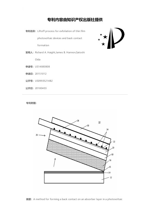
专利名称:Liftoff process for exfoliation of thin film photovoltaic devices and back contact f or mat ion
发明人:Richard A. Haight,James B. Hannon,Satoshi Oida
申请号:US14 880808 申请日:20151012 公开号:US09935214 B 2 公开日:201804 03 专利附图:
摘要:A method for forming a back contact on an absorber layer in a photovoltaic
பைடு நூலகம்
device includes forming a two dimensional material on a first substrate. An absorber layer including Cu—Zn—Sn—S(Se) (CZTSSe) is grown over the first substrate on the two dimensional material. A buffer layer is grown on the absorber layer on a side opposite the two dimensional material. The absorber layer is exfoliated from the two dimensional material to remove the first substrate from a backside of the absorber layer opposite the buffer layer. A back contact is deposited on the absorber layer.
静电成像方式英语作文
静电成像方式英语作文Title: The Principle and Applications of Electrostatic Imaging。
Electrostatic imaging, a technique utilized in various fields including medical diagnostics, security screening, and scientific research, relies on the manipulation of electrostatic forces to generate images. This essay delves into the principle behind electrostatic imaging, its applications, and the advancements in this technology.### Principle of Electrostatic Imaging。
Electrostatic imaging operates on the fundamental principle of electrostatic attraction and repulsion. It involves the creation of an electric field between acharged object and a grounded substrate. When an object is charged, the electric field interacts with nearby particles, causing redistribution of charges and resulting invariations in the electric potential across the surface. Bymeasuring these potential differences, an image of theobject's surface or internal structure can be reconstructed.### Components of Electrostatic Imaging Systems。
A Uniform Residence Time Flow Cell for the Microreactor-Assisted Solution Deposition of CdS
B. K. Paul,*,† C. L. Hires,† Y.-W. Su,‡ C.-H. Chang,‡ S. Ramprasad,§ and D. Palo§,∥
© 2012 American Chemical Society
■
deposition to resolve the temporal evolution of reaction chemistry. Under continuous flow conditions, byproducts and precipitates can be swept through the reaction chamber and reaction conditions can be kept constant and optimized with respect to time.4 It has been shown that microreactors can improve material yield and decrease solvent usage in comparison to typical CBD reactor conditions.5−7 Prior work showed results from a continuous flow microreactor using mL/h flow rates to increase the efficiency and conversion of [Zn2+] to ZnO nanowires.8,9 This occurs due to the greatly reduced diffusion times experienced in submillimeter diameter channels. Interference pattern measurements showed spatial variation in the ZnO nanowire length due to faster growth near the inlet of the reaction chamber and slower growth near the end as the bulk fluid neared depletion of active species. In addition, a distinct parabolic growth rate pattern can be seen as the fluid traveled faster down the axial center regions in comparison to the outer edges of the reactor. They also inverted the positioning of their flow cell, placing the substrate on the top surface to allow precipitating species to settle away from the growing ZnO wires. In this paper, we report the development of a high flow rate continuous flow MASD reactor to deposit CdS films over large substrates that compensates for lateral flow variation across a single high-aspect-ratio flow cell. Although much prior work has
Control of temperature uniformity during the manufacture of stable thin-film photovoltaic devices
Control of temperature uniformity during the manufacture ofstable thin-film photovoltaic devicesChetan P.Malhotraa,b,c,Roop L.Mahajan b,*,W.S.Sampath d ,Kurt L.Barth d ,Robert A.Enzenroth daInternational Centre for Science and High Technology,Trieste,ItalybDepartment of Mechanical Engineering,University of Colorado at Boulder,Campus Box 427,Boulder,CO 80309-0427,United StatescTata Research Development and Design Centre,Pune 411013,India dColorado State University,Fort Collins,CO 80521,United StatesReceived 16August 2005;received in revised form 16February 2006Available online 24April 2006AbstractThe production of stable thin-film photovoltaic cells requires tight control of temperature uniformity within the glass substrates dur-ing the vacuum deposition process.Though traditional approaches such as radiation shielding and channeling more power to outer lamps result in substantial improvements in temperature uniformity they fail in meeting the stringent requirement of less than 1°C variation across the substrate required to guarantee the long-term stability of the devices.The problem becomes especially acute while scaling up to larger commercially-viable panel sizes.To this end,a finite element thermal model of a commercial-scale deposition station has been developed and optimized with the target of achieving the desired temperature uniformity of 1°C.The effects of improvements such as radiation shielding,addition of radiation spreader,contouring of radiation spreader and optimizing power distribution among the radiation lamps have been studied.A new lamp configuration has been proposed for attaining the desired uniformity levels.Ó2006Elsevier Ltd.All rights reserved.Keywords:Photovoltaic cells;Vacuum deposition;IR heating;Thermal modeling and optimization1.IntroductionSolar energy holds the promise of becoming a cleaner alternative to fossil fuels.Although the price of crystalline silicon solar cells has dropped considerably in past few years [1],even cheaper methods of harnessing solar energy are required in order for it to attain commodity level adoption.To this end,a variety of alternative solar panel technologies such as amorphous silicon,CdTe and Cu(In,Ga)Se 2are being developed by research groups worldwide [2].Of these,solar panels fabricated by depositing thin films of cadmium telluride (CdTe)and cadmium sulfide on glass panels have shown a definite potential to replacecrystalline silicon [3]as the dominant solar material and a number of processes for developing CdTe solar cells have been developed [4].So far,the major impediment to suc-cessful demonstration of this technology has been the low device stability [5–7].Recently Sampath and co-workers [8–10]have demonstrated the production of stable CdTe solar panels in their pilot-scale manufacturing facility for 76mm ·76mm (300·300)solar panels.A schematic of this facility is shown in Fig.1.The facility is a continuous inline physical vapor deposi-tion system where all the device fabrication steps are per-formed in one vacuum enclosure.These steps include heating of the glass substrate,deposition of CdS and CdTe films,heat treatment with CdCl 2,ohmic contact formation and ohmic contact heat treating.The system is operated at 40mTorr of N 2.The processing stations are nearly identi-cal in design and construction.Devices produced using the0017-9310/$-see front matter Ó2006Elsevier Ltd.All rights reserved.doi:10.1016/j.ijheatmasstransfer.2006.02.042*Corresponding author.Tel.:+13034927750;fax:+13034923498.E-mail address:mahajan@ (R.L.Mahajan)./locate/ijhmtabove pilot system have been subject to accelerated indoor testing and have demonstrated a consistent efficiency of 10.5%over 7500h of operation.After successful demon-stration of the pilot system for manufacturing 76mm ·76mm (300·300)substrates,the facility is being scaled up to produce commercially viable 406mm ·406mm (1600·1600)panels.The stability of cells produced by the vapor deposition process is strongly related to the uniformity of deposition of the thin films on the glass substrate [11].The kinetics of the deposition process being a strong function of tem-perature,the uniformity of deposition directly depends on the temperature uniformity within the substrates [12,13].In order to consistently produce stable devices,the variation of temperature across the substrate is to be maintained below 1°C for a nominal temperature of 500°C [11].Simulations show that even without design optimization,the temperature variation within the sub-strate in the 76mm ·76mm (300·300)pilot facility of Sam-path et al.[9]was within 1°C and hence resulted in the production of stable devices.However,a model of the 406mm ·406mm (1600·1600)facility shows that the unop-timized variation across the substrate is 17.4°C which would have a pronounced deleterious effect on the device performance and stability.Hence it was decided to proac-tively optimize the 406mm ·406mm (1600·1600)facility to ensure high temperature uniformity before it was employed to manufacture solar panels.The design improvements considered include traditional approachessuch as radiation shielding and providing higher power to the outer lamps which are shown to greatly reduce the tem-perature variation within the substrate but fall short of meeting the target uniformity.A new lamp configuration with optimized power distribution is shown to be effective in reducing the temperature variation across the substrate to the low levels required for manufacturing stable photo-voltaic devices.The paper is organized as follows:(i)Section 2outlines the geometry of the deposition station.(ii)Section 3gives the details the finite element modeland its experimental validation.(iii)Section 4presents the simulations and results of theoptimization study.(iv)Section 5discusses the new lamp configuration toachieve the desired uniformity levels.(v)Section 6summarizes the findings of the study.2.GeometryThe schematic of a 406mm ·406mm (1600·1600)pro-cessing station is shown in Fig.2.It consists of two identi-cal graphite sources heated by two banks of seven quartz IR lamps.Each source is a 457mm ·457mm ·76mm (1800·1800·300)block with a 406mm ·406mm (1600·1600)central cavity.The cavity in the lower sourcehousesFig.1.Schematic of the pilot system for CdTe PV fabrication:(1)belt conveyor,(2)glass substrate,(3)air to vacuum to air (AVA)seal,(4)vacuum chamber,(5)heating module,(6)CdS deposition,(7)CdTe deposition,(8)CdCl 2deposition and heat treatment,(9)CdCl 2annealing and stripping,(10)ohmic contact formation,(11)contact annealing,(12)AVA seal,(13)completed seal.Nomenclature A area of surface in m 2C p specific heat in J/kg KF view factor between surfaces K thermal conductivity in W/m Kq radiation flux incident on surface in W/m 2Ttemperature in °CGreek symbolse emissivity of surface q density in kg/m 3r Stefan–Boltzmann constant (W/m 2K 4)Subscripts i surface index for cavity radiation calculations j surface index for cavity radiation calculationsC.P.Malhotra et al./International Journal of Heat and Mass Transfer 49(2006)2840–28502841the material to be deposited.The material sublimes and condenses on the underside of a glass substrate placed between the two sources to form the thin-film p–n junction of the solar cell.The IR lamps are housed in lamp holders made of electrically insulating silica material.A stainless steel backplate reflects radiation from the lamps back towards the sources.The end view also shows radiation shields and a heat spreader which will be discussed later in this document.3.Finite element modelThe complexities inherent in the geometry and the non-linear property variation preclude accurate quantification of the uniformity using analytical approaches.Hence,the finite element approach was employed to develop the ther-mal model of the station.Since the transport processes in the current study occur in near vacuum,it is assumed that heat transfer within the system only takes place by radia-tion exchange between the exposed surfaces and by con-duction through the solid sections.The nonlinearfinite element software ABAQUS was selected for developing the model since it has a built-in solver for cavity radiation and permits the solution of coupled transient radiation–conduction problems with nonlinear property variation. Since the geometry is symmetric about midplanes in all three Cartesian directions,only1/8th of the geometry needs to be modeled by assigning symmetry boundary con-ditions along the midplanes.Bounding surfaces were added to the top,back and side of the model to represent the vacuum chamber and provide boundary conditions for cavity radiation.Bounding sur-faces on the top and back were assigned a uniform temper-ature of70°C which is representative of values measured in the chamber walls of the pilot scale system.It is to be noted that in the actual setup,each station will have similar sta-tions adjacent to it on its two sides.Since the current model is representative of any given station it is assumed that the adjacent station is at a temperature not much different from the current station.Hence,a zeroflux or symmetry boundary condition is applied to the surfaces on the side of the model.The model is meshed using a combination of shell and brick heat transfer elements.Since the length to thickness ratio of the substrate is very large,to prevent loss of accu-racy associated with high aspect ratio solid elements or an inordinatelyfine mesh dictated by the small thickness of the substrate,the substrate was meshed using four noded shell elements which account for temperature variations in the thickness direction by numerical integration.The lamps too were meshed as2.54mm(0.100)thick hollow shells to closely represent the actual geometry of the IR quartz lamps being used.All the other components(except the radiation shields and the heat spreader)shown in Fig.2 were meshed using solid eight noded heat transfer brick ele-ments.Temperature dependent properties were supplied for all materials in the model.These are summarized in Tables A.1–A.5in Appendix.2842 C.P.Malhotra et al./International Journal of Heat and Mass Transfer49(2006)2840–2850The cavity radiation formulation in ABAQUS is based on the gray body assumption with diffuse reflection [14].Each exposed face of an element is considered as an iso-thermal,isoemissive surface.The emissivities assigned to the various materials considered in the model are given in Table A.6in Appendix .View factors between individual facets are calculated using the basic formula,F ij ¼Z A i ZA j cos /i cos /jp R 2d A i d A jwhere,d A i and d A j are the areas of the facets,R is the dis-tance between their centers and /i ,/j are the angles be-tween the line connecting the centers of the two facetsand their respective normals.The view factor calculation algorithm in ABAQUS also takes into account general sur-face blocking (or shadowing)as well as the most common forms of radiation symmetry.The current model uses the planar symmetry module in ABAQUS across the three Cartesian directions.The cavity radiation flux entering each facet of the cavity is calculated using the formula,q i ¼re i A i X je j X k F ik C À1kj ððT j þ273:15Þ4ÀðT i þ273:15Þ4Þwhere C ij ¼d ij Àð1Àe i ÞA iF ijand d ij is the Kronecker delta.The cavity radiation flux is converted into nodal fluxes and applied to the exposed nodes.To simulate heating from the IR lamps,a surface flux was applied to the outer surface of the lamp shells.The magnitude of the surface flux multiplied by the total sur-face area of the lamps was taken as the power input to the lamps.The steady-state solver in ABAQUS was invoked and the solution was assumed to be converged when the maximum residual heat flux in the model was below 0.5%.Each calculation took approximately 3h.When the mesh was refined by approximately 1.5times the maximum difference in temperature at points of interest in the source and substrate changed by only 0.3%while the computational time increased to 15h.Since the changes in temperature were within 1%while the increase in computa-tional time was approximately 5-fold,the basic mesh was used in this study.A mesh refinement of over 1.5times exceeded the 3GB memory capacity of the machine and could not be attempted.Experimental trials were conducted on an actual pro-cessing station similar to the one shown in Fig.2.The power input to the bottom lamps was adjusted to bring the temperature at the center of the pocket in the bottom source to approximately 400°C.With the temperature in the center of the pocket at $400°C,the temperatures at the rear and side of the pocket as well as that at the center of the top source were recorded.The experiment was car-ried out for two configurations:(i)without any radiationshields on the top source and (ii)with radiation shields on the periphery of the top source.These two experiments were simulated using the finite element method described above.A comparison of the results from the two experi-ments and the corresponding values from the finite element model is given in Table 1.As seen from the table,the pre-dictions of the model are within about 1%of the experi-mental data.The good agreement between the predictions of the finite element model and the experimental data established the validity of the modeling approach and the thermophysical properties used,in capturing the thermal transport in the actual system.Hence the modeling approach was used further for optimizing the processing station for minimum temperature variation within the substrate.4.Simulations and optimizationUsing the configuration shown in Fig.2,simulations were carried out to get the unoptimized temperature varia-tion within the substrate.The lamp power was adjusted to obtain a target temperature of 500±0.3°C at the center of the substrate.The largest temperature difference in the sub-strate is obtained between the center and the corner and was found to be 17.4°C.This is the baseline unoptimized temperature variation over which improvements were sought.The unoptimized power consumption was 2kW.Three methods traditionally used in the vacuum indus-try for reducing temperature variation were successively applied to the unoptimized geometry in order to improve the temperature uniformity within the substrate.First,radiation shields were added to the front and back of the source in order to prevent heat loss from the source to the chamber walls and thereby improve the uniformity within the source.Since the substrate is in very close prox-imity to the sources and gets heated via radiation from them,it can be expected that a reduction in temperature variation within the source would result in a corresponding reduction in temperature variation within the substrate.Second,a radiation spreader was added between the lamps and source to distribute the heat from the lamps uniformly to the top surface of the source.The spreader geometry itself could be optimized for maximizing uniformity.Table 1Comparison of predictions of finite element model with experimental resultsBottom source Top source CenterSide Rear Corner Center Experiment(with top shields)399386391384224Finite element model 399389.6393.8386.5226.7Error (%)0.90.70.6 1.2Experiment(without top shields)401–394388267Finite Element Model 401391.4396.4389.6264.4Error (%)–0.60.41.0C.P.Malhotra et al./International Journal of Heat and Mass Transfer 49(2006)2840–28502843Finally,the lamps could be wired separately and the power distribution across the lamps could be changed to obtain an optimum power distribution across the lamps which results in the maximum uniformity.The results of applying these three methods for improving the thermal uniformity are presented below.4.1.Addition of radiation shieldsRadiation shields in the form of1mm(0.0400)thick stainless steel plates were added at the back of the source as shown in Fig.2.The dimensions of the radiation shields were same as those of the face of the source and they were placed at a distance of1.5mm(0.0600)from each other.Due to the large length to thickness ratio of the shields,as with the substrate,they too were meshed with four noded shell elements.Since the shields were located in close proximity to each other,it was assumed that the view factor between adjacent radiation shields was1and hence the simpler gap radiation formulation in ABAQUS was applied to the spaces between the radiation shields which is given by the stan-dard formula,q¼rððT Aþ273:15Þ4ÀðT Bþ273:15Þ4Þ1=e Aþ1=e BÀ1where the suffixes A and B represent two adjacent shields.For a given value of power supplied to the lamps,with every additional radiation shield,the substrate temperature increased due to the lowering of heat loss from the sources. The power supplied to the lamps was incrementally reduced till the temperature at the center of the substrate was brought back to500±0.3°C.The difference between the maximum and minimum temperatures within the sub-strate was recorded as the maximum temperature variation within the substrate.This variation was plotted as a func-tion of number of radiation shields and is shown in Fig.3.The power required to maintain the substrate at 500°C with the addition of radiation shields is also shown in Fig.3.Two important deductions can be made from Fig.3. First,the addition of a single shield results in the maximum reduction in power input and also results in the maximum decrease in temperature variation from17.4°C to5.5°C. The relative improvement with additional shields is small and beyond15shields,the incremental reduction in power or temperature variation is negligible.The configuration with15radiation shields was therefore accepted as opti-mum at which the maximum temperature variation within the substrate was3.3°C and the power consumption was 0.89kW.In conclusion,the addition of radiation shielding results in a significant drop in temperature variation from 17.4°C to3.3°C.4.2.Addition of radiation spreaderIn order to further decrease the temperature variation within the substrate,a radiation spreader in the form of a3.2mm(1/800)stainless steel plate was added between the lamps and the source as shown in Fig.2.It was theo-rized that adding the spreader would provide a more uni-formly distributed source of heat addition as opposed to the discrete lamps and also serve to reduce heat loss from the top edges of the source to the lamp holder.How-ever,the effect of the heat spreader was not very large.Its addition reduced the maximum temperature variation within the substrate from3.3°C to2.7°C while the power consumption increased from0.89kW to0.92kW.Next,we sought to optimize the spreader geometry to see if any further improvements in uniformity could be obtained.Changing the thickness of the spreader from 3.2mm(1/800)to6.4mm(1/400)resulted in no significant improvement in the temperature variation(only0.05°C). The effect of using a spreader area smaller than the source area was studied next.The motivation behind contouring the spreader was to direct more heat towards the back of the source from where the main heat loss takes place. Fig.4shows the effect of increasing the gap between the edge of the spreader and the heater holder.As can be seen from thefigure,the curve shows a minimum at a gap of 76.2mm(300).However,the difference between the mini-mum temperature difference(2.64°C)and the temperature difference with a full spreader(2.67°C)is again insignifi-cant.Moreover,decreasing the spreader width on the sides always resulted in increase in the temperature variation within the substrate.Hence,it was concluded that contour-ing the spreader provides no significant benefit over the use of a spreader that completely shields the lamps from the source.The reason for this lack of improvement was due to the fact that though the a gap on the back of the source directed incrementally more radiativeflux there,it also exposed the top edges of the source directly to the heater holder to which they lost heat.These effects balance at the optimum spreader gap of76.2mm(300)but no overall improvement is obtained.2844 C.P.Malhotra et al./International Journal of Heat and Mass Transfer49(2006)2840–28504.3.Optimum power distribution among lampsA common method in obtaining temperature uniformity in rapid thermal processing(RTP)systems is to individu-ally control the power input to each heating lamp [15–22].This approach was adopted here to further improve the temperature uniformity within the substrate. In order tofind the power input to each lamp so that the maximum possible uniformity would be realized,an opti-mization program DN0ONF from the mathematical library IMSL[23]was interfaced to ABAQUS.This pro-gram is based on a FORTRAN subroutine NLPQL devel-oped by Schittkowski[24]and employs the successive quadratic programming method to solve general con-strained nonlinear programming problems.Tofind the optimum power distribution,this problem was specified as minimize fðx iÞwherefðx iÞ¼T substrate-maxÀT substrate-minand x i’s are power inputs to individual lamps subject to, T substrate-mid-500j j P0:3and06x i650The maximum lampflux was limited to50W/in.2corre-sponding to the maximum output of1500W per lamp. The equality constraint on the temperature at the center of the substrate was converted to the inequality constraint with a tolerance of±0.3°C to speed up the optimization process.Each evaluation of f(x i)required one simulation in ABAQUS.Since most of the computational effort in a simulation was consumed in the calculation of view factors which did not change in this part of the study,an interfac-ing program was written which updated the lampfluxes and obtained the substrate temperatures without exiting the ABAQUS run;the interfacing program then used re-verse communication to update the work function and con-straints in the optimizer.The unoptimized and optimum lamp power distribu-tions are shown in Fig.5.The optimization of the lamp powers for maximizing uniformity at a nominal tempera-ture of500°C resulted in reduction of the maximum temperature variation within the substrate from2.7°C to 2.5°C and the total power consumption remained unchanged at0.92kW.Even after optimizing the power distribution to the lamps,only a slight improvement in uni-formity was obtained.This indicated that the heating con-figuration shown in Fig.2was inherently inadequate in meeting the target temperature variation of below1°C required for producing stable thinfilm photovoltaics and a change in lamp configuration was necessary to obtain further improvement in uniformity.Hence a new lamp con-figuration was sought.5.New lamp configurationIn order to gain insight into the effect of various improvements discussed above on the temperature varia-tion within the substrate,the temperature contours within the substrate were plotted and are presented in Fig.6.As can be seen from thefigure,in the unoptimized configura-tion,the temperature within the substrate rapidly decreases from500°C at the center to482.6°C at the corner.Addi-tion of radiation shields substantially prevents heat loss from the front and back of the source thus significantly improving the uniformity within the substrate.The maxi-mum and minimum temperatures yet occur at the center and corner respectively.Addition of a spreader between the lamps and the source serves to reduce the temperature gradients within the substrate.Optimization of power dis-tribution among the lamps directs the power to the outer lamps which moves the location of the maximum tempera-ture from the center of the substrate to the side of the sub-strate.This serves to direct the majority of the heatflow through the radiation shields as opposed to the corner ofC.P.Malhotra et al./International Journal of Heat and Mass Transfer49(2006)2840–28502845the source thereby further reducing the temperature varia-tion.The above temperature contours indicate that further improvement in uniformity can only be obtained by actively restricting the heat flow from the front and back of the source.Passive shields can only achieve this up to a point.Hence,it was decided to place an active source of heat i.e.an IR lamp instead of the radiation shields in front and back of the source as shown in Fig.7.Three different optimization studies were undertaken after adding the extra lamp at the front and back of the sources.In the first study,all the lamps were assigned the same amount of power.This is the easiest configuration from an ease-of-control perspective.With all lamps draw-ing the same power,the maximum temperature variation was found to be 2.6°C which is only marginally better than 2.7°C obtained for the case with radiation shields,no front and back lamps,and uniform power distribution among top and bottom lamps.The total power consumption how-ever increased from 0.92kW to 1.35kW.In the second study,the top and bottom lamps were assigned the same power while the front and back lamps were assumed to be controlled independent of them.In this case,the maxi-mum variation within the substrate dropped to 1.2°C while the overall power consumption increased to 1.42kW.Out of this only 0.61kW was consumed by the 14top and bottom lamps while the rest (0.81kW)was con-sumed by the four front and back lamps.The uniformity so obtained was within reach of the target of 1°C.In the last study,the power supply to every lamp was varied indepen-dently.This resulted in a maximum variation of only 0.65°C.The total power drawn by the system was 1.42kW.Of this the optimizer directed 0.75kW to thefourFig.6.Temperature contours within substrate with increasing uniformity.2846 C.P.Malhotra et al./International Journal of Heat and Mass Transfer 49(2006)2840–2850front and back lamps,0.6kW to the four edge lamps in the top and bottom and a small amount(0.06kW)to the two middle lamps in the top and bottom.The rest of the lamps i.e.the inner lamps in the top and bottom with the excep-tion of the middle lamps drew no power.Thus it can be concluded that the inner lamps in the top and bottom areFig.8.Temperature contours within substrate for three optimization studies with front and back lamps instead of radiation shields.C.P.Malhotra et al./International Journal of Heat and Mass Transfer49(2006)2840–28502847redundant i.e.effective heating and control of thermal uniformity within the substrate can be obtained by only the four edge lamps on the top and bottom of the sources and the4lamps in the front and back of the two sources.The temperature contours obtained within the substrate in the above three studies are presented in Fig.8.The gen-eral nature in temperature contours is largely unchanged between Figs.6c and8a and the temperature uniformity is almost identical in both cases indicating that though the addition of front and back lamps can be an impediment to heatflow from the front and back surfaces of the sources (as was the case with the radiation shields for Fig.6c),the constraint that they have the same power as the top lamps is too restrictive and does not alter the general nature of heatflow in the problem.Fig.8b shows a considerable departure from the general problem in that it shows that heating from the front and back lamps is preferable toheating from the top and bottom lamps for achieving higher thermal uniformity within the substrate.This is also concluded from the fact that a majority of the power is directed to the front and back lamps as opposed to the top and bottom stly Fig.8c shows that the most optimized heating configuration for the current problem distributes power to the front and back lamps and the outer or edge lamps in the top and bottom banks thus pro-viding the most symmetric temperature distribution within the substrate permitted by the problem.6.SummaryThe fabrication of stable thinfilm CdTe photovoltaic cells necessitates tight control of temperature uniformity within the substrate during the vacuum deposition process. Though the configuration for producing76mm·76mm (300·300)panels meets these uniformity requirements,on scaling the panel size to406mm·406mm(1600·1600)it is no longer possible to achieve the desired uniformity levels even after employing traditional methods such as radiation shielding and directing more power to the outer lamps.Hence it is necessary to employ computer based optimization techniques for maximizing the temperature uniformity.To this end,afinite element model of a single processing station was developed,interfaced to a numerical optimization routine in IMSL,and the effect of various uniformity enhancement techniques was studied.Thefind-ings of the study are summarized in Table2.It can be con-cluded that while passive shielding and optimizing the power distribution to different lamps can substantially improve the thermal uniformity in the substrate,they can-not alter the basic heatflow patterns in the graphite sources and thus a temperature gradient always exists between the center and the rear of the sources.Addition of an active heat source(IR lamps)in the front and back of the graph-ite sources and then optimizing the power input to all the lamps results in a heatflow pattern that directs heat from the peripheral lamps towards the center of the source and results in a maximum variation of only0.65°C within the substrate which is well within the target value of1.0°C.The optimization study also indicates that the inner lamps in the top and bottom banks are redundant and can be safely removed without loss in thermal uniformity.AcknowledgementThe authors gratefully acknowledge the partial funding extended by the International Center for Science and High Technology(ICS),Trieste,Italy.Appendix.Thermophysical properties of materials used in finite element modelTables A.1–A.6.Table2Summary offindings of optimization studyConfiguration Max temperaturevariation insubstrate(°C)Total powerconsumption(kW)Basic17.4 2.00Add15radiation shields 3.30.89Add spreader 2.70.92 Optimize spreader geometry 2.60.91 Optimize power distributionamong lamps2.50.92Add front and back lamps(remove shields)samepower to all lamps2.6 1.35Different power levels totop/bottom and front/backlamp banks1.2 1.42Different power levels to all lamps0.65 1.42Table A.1Properties of graphite sources[25]T(°C)K(W/m K)T(°C)C p(J/kg K)q(kg/m3) 011026.85721.41700 2008576.8587540072126.851025.860062176.851155.680055226.851268.6100050276.851352.3120045326.851423.5140041376.851490.5160038426.851549.2476.851599.4526.851645.4576.851683.1626.851712.4676.851737.5726.851762.6826.851808.7926.851854.71026.851892.42848 C.P.Malhotra et al./International Journal of Heat and Mass Transfer49(2006)2840–2850。
摩尔酮磷酸钴粉产品说明书

Revision: 000 Date: 19 May 20031. IDENTIFICATION OF THE SUBSTANCE AND COMPANYUNDERTAKINGGeneral Chemical Name MOLYBDENUM NITRIDE powderIntended/recommended use: ResearchSupplier (Distributor): New Metals & Chemicals Ltd.Newmet House, Rue de St. LawrenceWaltham Abbey, Essex, EN9 1PFTelephone +44 (0)1992 7111112. COMPOSITION/INFORMATION ON INGREDIENTSIngredient Name Concentration Classification* CAS number EINECS No.-------------------------------------------------------------------------------------------------------------------------------------------- Molybdenum nitride 100% Xn: R48/20/22 12033-01-1Xi: R36/37/38*see 16. OTHER INFORMATION for full text of R-phrases.3. HAZARD IDENTIFICATIONDanger of serious damage to health by prolonged exposure through inhalation and ifswallowed.Irritating to eyes, respiratory system and skin.4. FIRST AID MEASURESInhalation If signs/symptoms like coughing or burning occur, remove person fromexposure to fresh air immediately and administer 100 percenthumidified supplement oxygen with assisted ventilation as required. Ifbreathing has ceased DO NOT use mouth-to-mouth respiration. Applyartificial respiration using oxygen and a suitable mechanical device suchas a bag and a mask. Seek immediate medical attention.Skin Contact Flush skin with large amounts of water. Remove contaminated clothing.If irritation persists, seek medical attentionEye Contact DO NOT allow patient to rub or keep eyes closed. Irrigate with copious quantities of water for at least 15 minutes. Flush under eyelids by liftinglid. DO NOT use a static eye bath. Seek immediate medical attention. Ingestion Induce vomiting if patient is conscious and alert. Give 2 cupfuls of milk with great care. Do not induce vomiting and give nothing by mouth ifpatient is unconscious. Seek immediate medical attention.5. FIRE FIGHTING MEASURESPrecautions against fire and explosionMaterial is non flammable but will react with water or steam to produce flammable,toxic and corrosive gas (ammonia).Use dry sand , dry salt, carbon dioxide or extinguishing powder. For large fires coolcontainers with flooding quantities of water until well after the fire is out. Do not getwater inside containers.Extinguishing media which must not be used for safety reasonsDO NOT USE water or foam, See above.Exposure hazards arising from substance, combustion products, resulting gases Molybdenum nitride will react with water to produce flammable, toxic and corrosivegas (ammonia).Molybdenum oxide particles may be formed in fire which are toxic and irritant.Nitrogen oxides may also be formed.Special protective equipment for fire fightersWear full protective clothing, including self-contained breathing apparatus.6. ACCIDENTAL RELEASE MEASURESPersonal Precautions:Remove or extinguish all ignition sources. Evacuate all but essential authorised control personnel. Wear self-contained breathing apparatus and gloves to avoid inhalation, skin and eye contact. Provide sufficient ventilation.Environmental PrecautionsPrevent entry into drains, surface and ground water, soil and confined areas.Methods for Cleaning upOnly trained, authorised personnel should be involved. Fully encapsulating protectiveclothing and self contained breathing apparatus should be worn for spills and leaks with no fire. Do not touch damaged containers or spilled material unless wearing appropriate protective clothing.Stop leak if you can do it without risk. Keep combustibles (wood, paper, oil etc) away from spilled material. Cover spills with dry sand, dry diatomaceous earth or dry salt followed with plastic sheet to minimise spreading or contact with water. Use clean non-sparking tools to collect material and place it into loosely covered plastic containers, suitably marked, and dispose of through a licensed disposal contractor.7. HANDLING AND STORAGEPrecautions for safe handlingTo be handled by qualified and trained staff only. Avoid breathing dusts and direct contact with skin and eyes. Avoid all contact with water. Wash hands thoroughly after handling. See section 8 for personal protective equipment.Handle under dry inert gas. Ensure good ventilation/exhaustion at the workplaceKeep ignition sources away - do not smokeProtect against electrostatic charges.Fumes can combine with air to form an explosive mixture.Precautions for safe storageKeep container cool, dry and tightly closed when not in use. Moisture sensitive.Store away from oxidisers and other materials listed under incompatibility (see section10).Specific useResearch.8. EXPOSURE CONTROLS/PERSONAL PROTECTIONExposure limit valuesIngredient name OES LTEL OES STEL MEL(LT) MEL(ST)(8 hr TWA) (15 min)Molybdenum compounds(as Mo) insoluble compounds 10mg/m320mg/m3The usual precautionary measures should be adhered to in handling chemicals. Keep awayfrom foodstuffs, beverages and food. Instantly remove any soiled and impregnated garments.Wash hands during breaks and at end of the work. Avoid contact with the eyes and skin. Occupational exposure controlsEye Protection Wear appropriate protective eyeglasses, chemical safety gogglesor full face shield to European Standard EN 166.Hand protection Wear appropriate gloves when handling this material. Suitablematerial is butyl rubber. However, due regard must be taken thatheavy gloves will interfere with the wearer’s sense to touch andmay contribute to a dangerous situation. Thinner gloves of nitrileand PVC may be used as disposable gloves and must bediscarded immediately after use. Gloves should comply withEuropean Standard EN 465-3 class 3.Skin Protection Use one or more of the following personal protection items asnecessary to prevent skin contact: Full chemical protective suitto EN 465 standard, PVC apron, helmet and boots.Respiratory Protection Avoid inhalation of dust. Select the following respirator basedon airborne concentration of contaminants: Full face dustrespirator. Half -mask air-supplied respirator to EN 147. Full-face high efficiency filter respirator to EN 147 or EN12941/12942. Full-face or hood compressed air breathingapparatus to EN 139 or EN 270/271. Use appropriate localexhaust ventilation, to maintain airborne exposure below controllimits. Ingestion: Do not eat, drink or smoke when using this product. Do notingest. Exhibit the strictest hygiene control.Environmental exposure controlsNo specific environmental legislation applies, however in accordance with best practise only use in a fume cupboard or with local exhaust ventilation, ventilated to a scrubbing system. In case of fire, spillage, or leakage, prevent material from entering water courses, sewers or soil. Material will decompose in air forming ammonia gas.9. PHYSICAL AND CHEMICAL PROPERTIESGeneral informationAppearance Black powderOdour Slight ammoniacal odourImportant health, safety and environmental informationpH N/ABoiling point/boiling range N/AMelting point/melting range N/AFlash point N/AFlammability (solid, gas) Non flammableAutoignition temperature N/AExplosive properties N/AOxidising properties Not oxidisingVapour Pressure N/ARelative density 9.06g/cm3 at 200CSolubilityWater Reacts10. STABILITY AND REACTIVITYStability Stable, but will decompose if exposed to moist air orwater.Conditions to avoid Avoid creating dusts. Air and moisture sensitive. Materials to avoid Avoid water, acids, oxidising agents.Hazardous Decomposition Products Will react with water at room temperature toproduce flammable/explosive and corrosive ammoniagas. Decomposition products include nitrogen oxidesand molybdenum oxides.11. TOXICOLOGICAL INFORMATIONMolybdenum nitride will react with water under normal conditions.Effects from eye contact May cause severe irritation and damage to the eyes.Symptoms include burns, irritation, redness andconjunctivitis. Repeated or prolonged exposure maycause irreversible damage to the conjunctiva, cornea andlens.Effects from skin contact May cause skin irritation and burns. Prolonged exposuremay cause tissue damage.Effects from inhalation May cause irritation to mucous membranes and upperrespiratory tract. Ammonia gas may cause irritation tothe nose and throat, dyspnea, bronchial spasms, chestpains, pulmonary edema and pink frothy sputum. Effects from ingestion Irritating to digestive tract. May cause acute orchronic molybdenum poisoning. Will decompose totoxic and corrosive ammonia causing secondary damage.Symptoms include abdominal pain, nausea, vomitingsoreness/redness of the mouth and throat, burns anddysphagia.(a) Acute toxicity (oral, inhalation, dermal) not tested/no data(b) Corrosive/irritation (eye, skin, respiratory tract) not tested/no data(c) Sensitisation (skin, respiratory) not tested/no data(d) Repeated-dose toxicity not tested/no data(e) Mutagenicity not tested/no data(f) Carcinogenicity not tested/no data(g) Reproductive toxicity not tested/no dataTo the best of our knowledge the chemical, physical and toxicological properties of molybdenum nitride have not been thoroughly investigated and recorded.Molybdenum compounds are toxic by subcutaneous and intraperitoneal routes. Molybenum and its compounds are highly toxic based upon animal experiments. Symptoms of acute poisoning include severe gastrointestinal irritation with diarrhoea, coma and death from heart failure. Experimental animals exposed to high levels accumulated molybdenum in the lungs, spleen and heart and showed a decrease of DNA and RNA in the liver, kidneys and spleen Many nitrides react with moisture to evolve ammonia which is a human poison by an unspecified route.12. ECOLOGICAL INFORMATION(1) Ecotoxicity(a) Aquatic toxicity(i) acute and chronic for fish not tested/no data(ii) acute and chronic for daphnia not tested/no data(iii) acute and chronic for algaefish not tested/no data(iv) acute and chronic for other aquatic plants not tested/no data(b) Soil toxicity(i) macro organisms not tested/no data(ii) micro organisms not tested/no data(iii) birds not tested/no data(iv) bees not tested/no data(v) plants not tested/no data(vi) fauna not tested/no data(2) MobilityThe product’s mobility is limited because it will react with water or air-moisture atroom temperature.(3) Persistence and degradabilityThe product will rapidly react with water or moisture and degrade.(4) Bioaccumulation potentialMolybdenum nitride cannot enter the food chain because it will immediately react with water and form toxic molybdenum oxide.(5) Other adverse effectsNo other effects are known.13. DISPOSAL CONSIDERATIONSAll waste material to be contained in a plastic sealed bin, duly marked, and disposed of as special waste through a licensed waste contractor in accordance with “The Special Waste Regulations 1996”. See sections 6 and 7.14. TRANSPORT INFORMATION(a) UN number 3288(b) class 6.1(c) proper shipping name: Toxic solid, inorganic, n.o.s. (molybdenumnitride(d) packing group III(e) marine pollutant (if applicable) N/A(f) other applicable information N/A15. REGULATORY INFORMATIONEC Supply: Chip-3 regulations 2002Xn: HarmfulXi: IrritantRisk Phrases:48/20/22: Harmful: danger of serious damage to health by prolonged exposure through inhalation and if swallowed.36/37/38: Irritating to eyes, respiratory system and skin.Safety Phrases:7/8: Keep container tightly closed and dry.22: Do not breathe dust.26: In case of contact with eyes, rinse immediately with plenty of water and seek medical adviceThis material is subject to the COSHH regulations 2002. See COSHH Essentials for further information.16. OTHER INFORMATIONR Phrases Full Text:48/20/22: Harmful: danger of serious damage to health by prolonged exposurethrough inhalation and if swallowed.36/37/38: Irritating to eyes, respiratory system and skinAbbreviations used:CAS Chemical Abstracts Service Registry NumbersEINECS European Inventory of Existing Commercial Chemical SubstancesMSDS Material Safety Data SheetHSE Health and Safety ExecutiveTWA Time Weighted AverageOES Occupational Exposure StandardsThis material should only be handled by qualified, trained chemists, fully familiar with its dangerous properties. During use or handling, a minimum of two persons should always be available.References:Chemicals (Hazard Information and Packaging for Supply) Regulations 2002Approved classification and labelling guide. Chemicals (Hazard Information andPackaging for Supply) Regulations 2002 Guidance on Regulations L131Approved Supply List. Information Approved for the Classification and labelling ofSubstances and Preparations Dangerous for Supply. Chemicals (Hazard I n formation and Packaging for Supply) Regulations 2002. Approved List L129Control of Substances Hazardous to Health Regulations 2002Health and Safety at Work Act 1974COSHH Essentials: Easy Steps to Control Chemicals. Control of Substances Hazardous to Health RegulationsOccupational Exposure Limits 2001/2002 EH40European Inventory of Existing Commercial Substances (EINECS) available on the European Chemicals Bureau website at www.ecb.jrc.it/existing- chemicalsFirst Aid at Work. The Health and Safety (First Aid) Regulations 1981. Approved Code of Practice and Guidance L74Personal Protective Equipment (EC Directive) Regulations 1992The Selection, Use and Maintenance of Respiratory Protective Equipment: A Practical Guide HSG53Cost and Effectiveness of Chemical Protective Gloves for the Workplace.Guidance for Employers and Health and Safety Specialists. HSG206Environmental Protection Act 1990 c43Environmental Act 1995 c25The Special Waste Regulations 1996The Dangerous Substances and Explosive Atmospheres Regulations 2002。
PS术语及操作指令中英对照

PS术语及操作指令中英对照以下是一些PS(Adobe Photoshop)的术语及操作指令的中英对照:1. File - 文件2. New - 新建3. Open - 打开4. Save - 保存5. Save As - 另存为6. Close - 关闭8. Undo - 撤销9. Redo - 重做10. Cut - 剪切11. Copy - 复制12. Paste - 粘贴13. Select - 选择14. Deselect - 取消选择15. Transform - 变换16. Image - 图像17. Adjustments - 调整18. Brightness/Contrast - 亮度/对比度19. Levels - 色阶20. Curves - 曲线21. Hue/Saturation - 色相/饱和度22. Shadows/Highlights - 阴影/高光23. Filters - 滤镜24. Blur - 模糊25. Sharpen - 锐化26. Distort - 动态27. Liquify - 液化28. Noise - 噪点29. Type - 文本30. Horizontal Type Tool - 水平文本工具31. Vertical Type Tool - 垂直文本工具32. Eyedropper - 吸管33. Clone Stamp - 图章34. Healing Brush - 治疗画笔35. Brush - 画笔36. Pencil - 铅笔37. Eraser - 橡皮擦38. Fill - 填充39. Gradient - 渐变40. Zoom - 缩放41. View - 视图42. Actual Pixels - 实际像素43. Fit on Screen - 适应屏幕44. Window - 窗口45. Layers - 图层46. Layer Style - 图层样式47. Blending Options - 混合选项48. Opacity - 不透明度49. Layer Mask - 图层蒙版50. Group - 群组51. Merge - 合并52. Flatten Image - 扁平化图像53. Filter - 滤镜54. Liquify - 液化55. Sharpen - 锐化56. Distort - 扭曲57. Adjustments - 调整58. Brightness/Contrast - 亮度/对比度59. Levels - 色阶60. Hue/Saturation - 色相/饱和度61. Image Size - 图像尺寸62. Canvas Size - 画布尺寸63. Image Rotation - 图像旋转64. Flip - 翻转65. Rotate - 旋转66. Perspective - 透视67. Crop - 裁剪68. Magic Wand - 魔术棒69. Lasso - 套索70. Quick Selection - 快速选择71. Pen - 笔工具72. Smudge - 涂抹工具73. Spot Healing Brush - 治疗画笔74. Clone Stamp - 图章75. Eraser - 橡皮擦76. Dodge - 避开77. Burn - 加深78. Blur - 模糊79. Sharpen - 锐化80. Sponge - 浸泡81. Text - 文本82. Move - 移动83. Eyedropper - 吸管84. Hand - 手形工具85. Zoom - 缩放86. Actual Pixels - 实际像素87. Fit on Screen - 适应屏幕88. Layers - 图层89. Layer Style - 图层样式90. Blending Options - 混合选项91. Opacity - 不透明度92. Layer Mask - 图层蒙版93. Group - 群组94. Merge - 合并95. Flatten Image - 扁平化图像96. File Format - 文件格式97.JPEG-JPEG98.PNG-PNG99.GIF-GIF100.PSD-PSD101.TIFF-TIFF102.BMP-BMP103.PDF-PDF104.EPS-EPS105. Targa - Targa106. Image Size - 图像尺寸107. Canvas Size - 画布尺寸108. Resolution - 分辨率109. Color Mode - 色彩模式110.RGB-RGB111.CMYK-CMYK112. Grayscale - 灰度113. Lab Color - Lab颜色114. Smart Objects - 智能对象115. Smart Filters - 智能滤镜116. Perspective Warp - 透视变形117. Content-Aware Fill - 以内容为基础的填充118. Content-Aware Move - 以内容为基础的移动119. Puppet Warp - 玩偶变形120. Vanishing Point - 消失点121. Camera Raw - 相机原始文件122. Panorama - 全景照片123. Stitch - 拼接124. Photomerge - 图片合并125.HDR-高动态范围126. High Dynamic Range - 高动态范围127. Blend Modes - 混合模式128. Normal - 正常129. Dissolve - 分解130. Darken - 变暗131. Multiply - 正片叠底132. Color Burn - 颜色加深133. Linear Burn - 线性加深134. Lighten - 变亮136. Color Dodge - 颜色减淡137. Linear Dodge - 线性减淡138. Overlay - 叠加140. Hard Light - 强光141. Vivid Light - 亮光142. Linear Light - 线性光143. Pin Light - 点光144. Hard Mix - 实色混合145. Difference - 差异146. Exclusion - 排除147. Hue - 色相148. Saturation - 饱和度149. Color - 色度150. Luminosity - 明度。
MicroChemicals GmbH TI xLift图像反转抗胀性胶类技术数据册-08 2016
TI xLiftimage reversal resistTechnical Data Sheetrevised 08/2016MicroChemicals GmbHNicolaus-Otto-Str. 39D-89079 UlmFon +49 (0) 731 977343 0Mobil +49 (0) 178 7825198Fax +49 (0) 731 977343 29Email ***********************Internet General InformationThe TI xLift image reversal resist is optimized for lift-off of thick to very thick (5 .. 20 m m) films.This technical data sheet intends to give you a guide-line for process parameters for various applications. However, the optimum values for e.g. spin profile, exposure dose, or development depend on the individual equipment and need to be adjusted on each individual demand.10 m m¬10.5 m m thick metal via lift-off with TI xLift'Image Reversal' – A Short IntroductionWhat 'image reversal' generally meansinverted mask (the exposed areas finally remain)behaves like an exposed positive resist.cross-links the exposed area, while the unexposed area remains photo-active(without mask) ...which was not exposed in the first step, soluble in developerareas exposed in the firststep now remain... and for what image reversal is good for: Adjustable undercut for lift-off of thin and thick sputtered, CVD, and evaporated films like metals, a-Si:H, a-SiN:H etc.®Processing the TI xliftIn chronological order:■After cleaning the substrate, put the substrate on the hotplate at minimum 120 °C for 10 minutes to remove adsorbed water from the substrate surface.Alternatively, you can use a furnace at same temperature for 30 min. Standard HMDS procedure (only from vapor phase with an optimum substrate temperature of 125°C !) is also an adequate preparation.■Spin-coat the resist immediately after cooling down the substrate at: resist thickness 5.9 m m 7.0 m m 8.2 m m 10.5 m m 14.4 m m 20.0 m m final rpm 2.200 1.600 1.400 1.200 900 600 with an acceleration of approx. 900 rpm/s and keep at final spin speed for 5 seconds. Then decelerate down to 0 rpm at approx. –900 rpm/sec. For 4 inch wafer, a minimum of 3.0 ml of resist is recommended.■Leave the substrate on the spin-coater (or on any horizontal surface at room temperature) for at least 5 min (»5 m m resist thickness) to 30 min (»20 m m resist thickness). This will smooth the surface, reduce striations, and allow the edge bead near the substrate edge i) to flatten and ii) to contract to the outermost few mm of the wafer. If subsequent soft-bake causes foaming or patterning of the resist, increase the delay.■Soft-bake at 95°C on a hot-plate or in an fufor:total resist thickness 5 .. 9 m m 10 .. 16 m m 17 .. 24 m m time (min) 20 40 60■Remove the edge bead on the edge of the substrate. We recommend giving a sharp stream of AZ EBR solvent (PGMEA) focused on the outer few mm of the substrate spinning at 1.000 rpm. Avoid spattering drops of EBR on the inner side of the substrate, this will cause spots with reduced resist thickness.■Exposure broadband or i-line (with the mask) at a (as calibrated on i-line, 365 nm) dose of approximately:total resist thickness 5.9 m m 7.0 m m 8.2 m m 10.5m m 14.4m m20.0m mfirst exposure dose (mJ/cm2) 40 ..10050 ..14080 ..200110 ..280150 ..400180 ..500= exposure time (sec.)(holds for all standard maskaligners with a 350W Hg-lamp)4 .. 105 .. 14 8 .. 20 11 .. 28 15 .. 40 18 .. 50This first exposure dose adjusts the final wall profile and can be increased/decreased by up to 50% for optimum results (see Appendix).■Post-exposure delay time:total resist thickness 5 .. 9 m m 10 .. 16 m m 17 .. 24 m m Room temperature 20° (min) ... 5 5 10... subsequent hot-plate 50°C (min) 0 15 30In this delay time, N 2, generated during exposure, will diffuse out the resist. If the resist foams on the hot-plate, next time increase the delay time at room temperature.■ Reversal Bake: After the delay bake the substrate at a temperature of 130°Con the hotplate for 2 minutes (when using furnace try 20 minutes at 120°C-130°C. Because this step is very temperature critical furnace baking is not recommended). This step is the reversal bake where the image is reversed due to cross link the exposed areas making them insoluble in the developer. If the resist foams, next time increase the delay time at 50°C (see previous point) ■ Flood Exposure: Exposure the substrate for the second time without a mask(flood exposure).total resist thickness 5 .. 9 m m 10 .. 16 m m 17 .. 24 m m dose (mJ/cm 2)» 800» 1.000» 1.200When, during a subsequent deposition, the temperature will raise over 80°C, use a high exposure dose to avoid nitrogen bubbles in the resist during the deposition. ■Develop e.g. in AZ 826MIF. When the structures are through-developed, add another approx. 10-30% of the time in the bath of development time to finalize the side wall profile (see appendix). Beside the used developer, development time depends on resist thickness and strongly on reversal bake temperature. If shorter development times are important, use AZ 400K 1:3.5 (e.g. 100 ml AZ 400K and 350 ml DI-water). Resist dark erosion might slightly increase.600900120015001800210046810121416182022r e s i s t t h i c k n e s s (m m )spin speed (rpm)Appendix A: Adjusting the undercutUndercut depends on:1.First exposure doseAt low 1st exposure doses, only the upper part of the resist is exposed. Only this region will subsequently be 'reversed' during image reversal bake. The substrate-near resist now is still unchanged and will be exposed (and made soluble) in the subsequent flood exposure. If the first exposure dose is too low, development will lift the upper resist layer, or/and the dark erosion is too high.® High 1st exposure dose: Reduced undercut2.Reversal bake temperature and reversal bake timeIf the reversal bake temperature- and time is too low, the image reversal process will not be completed. As a consequence, the resist exposed during the 1st exposure shows a high 'dark erosion' during development, sometimes appearing as holes or bubbles in the resist. With increasing reversal bake temperature/-time, the reversal process improves, and dark erosion is reduced.At reversal bake temperatures/-times chosen to high, even the parts of the resists exposed by scattered light during the 1st exposure (in regions where no light should be) are reversed. As a consequence, the profile might change from the desired undercut to a typical positive profile.® High reversal bake temperature/-time: Reduced undercut3.Developer/Development timeWith increased developing time, or by the usage of strong developers (like AZ 400K in dilutions of 1:3.5 and stronger), also the parts of the resist are developed, where the image reversal process has been performed.® High developing time: Increased undercutAppendix B: Parameters and profileExample I: Varying the first exposure dose at 30% 'over-developing'(Thickness 12 m m; Rev. bake 130°C 2min; Flood exp. 1.000 mJ; Dev. AZ400K 1:3, 8 min)1st exp. 85 mJ/cm 2 170 mJ 260 mJ430 mJExample II: Varying the development time at low first exposure dose(Thickness 15 m m; 1st exp. 240 mJ, Rev. bake 130°C 2min; Flood exp. 1.200 mJ; Dev. AZ400K 1:2.5)Dev. time 5.0 min 6.5 min 8.5 min 15 minExample III: Varying the development time at high first exposure dose(Thickness 13 m m; 1st exp. 310 mJ, Rev. bake 130°C 2min; Flood exp. 1.200 mJ; Dev. AZ400K 1:2.5)Example IV: Varying the reversal bake(Thickness 11 m m; Rev. bake 130°C; Flood exp. 1.000 mJ; Dev. AZ 826MIF)rev. bake time 1 min 6 min11 mue。
EN 61853-1-2011 PV module performance testing and energy rating - Part 1
ICS 27.160
EN 61853-1
March 2011
English version
Photovoltaic (PV) module performance testing and energy rating Part 1: Irradiance and temperature performance measurements and power rating (IEC 61853-1:2011)
-2-
Foreword
The text of document 82/613/FDIS, future edition 1 of IEC 61853-1, prepared by IEC TC 82, Solar photovoltaic energy systems, was submitted to the IEC-CENELEC parallel vote and was approved by CENELEC as EN 61853-1 on 2011-03-02. Attention is drawn to the possibility that some of the elements of this document may be the subject of patent rights. CEN and CENELEC shall not be held responsible for identifying any or all such patent rights. The following dates were fixed: – latest date by which the EN has to be implemented at national level by publication of an identical national standard or by endorsement – latest date by which the national standards conflicting with the EN have to be withdrawn Annex ZA has been added by CENELEC. __________
Photovoltaic Power Generation
PHOTOVOLTAIC POWER GENERATIONABSTRACTThis report is an overview of photovoltaic power generation. The purpose of the report is to provide the reader with a general understanding of photovoltaic power generation and how PV technology can be practically applied.There is a brief discussion of early research and a description of how photovoltaic cells convert sunlight to electricity. The report covers concentrating collectors, flat-plate collectors, thin-film technology, and building-integrated systems. The discussion of photovoltaic cell types includes single-crystal, poly-crystalline, and thin-film materials. The report covers progress in improving cell efficiencies, reducing manufacturing cost, and finding economic applications of photovoltaic technology. Lists of major manufacturers and organizations are included, along with a discussion of market trends and projections.The conclusion is that photovoltaic power generation is still more costly than conventional systems in general. However, large variations in cost of conventional electrical power, and other factors, such as cost of distribution, create situations in which the use of PV power is economically sound. PV power is used in remote applications such as communications, homes and villages in developing countries, water pumping, camping, and boating. Grid-connected applications such as electric utility generating facilities and residential rooftop installations make up a smaller but more rapidly expanding segment of PV use. Furthermore, as technological advances narrow the cost gap, more applications are becoming economically feasible at an accelerating rate.INTRODUCTIONThis report is the result of Gale Greenleaf’s October 19, 1998 request for proposal. Bill Louk and Tom Penick responded to her request with a proposal, dated October 30, 1998, to continue earlier research on photovoltaic power generation. The proposal was approved and resulted in continued research followed by a presentation on November 30, 1998 and this final report on photovoltaic power generation.PHOTOVOLTAIC TECHNOLOGY Scientists have known of the photovoltaic effect for more than 150 years. Photovoltaic power generation was not considered practical until the arrival of the space program. Early satellites needed a source of electrical power and any solution was expensive. The development of solar cells for this purpose led to their eventual use in other applications.DISCOVERY AND DEVELOPMENT OF PHOTOVOLTAIC POWERThe photovoltaic effect has been known since 1839, but cell efficiencies remained around 1% until the 1950s when U. S. researchers were essentially given a blank check to develop a means of generating electricity onboard space vehicles. Bell Laboratories quickly achieved 11% efficiency, and in 1958, the Vanguard satellite employed the first practical photovoltaic generator producing a modest one watt.In the 1960s, the space program continued to demand improved photovoltaic power generation technology. Scientists needed to get as much electrical power as possible from photovoltaic collectors, and cost was of secondary importance . Without this tremendous development effort, photovoltaic power would be of little use today.POWER OUTPUT AND EFFICIENCY RATINGSThe figures given for power output and efficiency of photovoltaic cells, modules, and systems can be misleading. It is important to understand what these figures mean and how they relate to the power available from installed photovoltaic generating systems.Power RatingsPhotovoltaic power generation systems are rated in peak kilowatts (kWp). This is the amount of electrical power that a new, clean system is expected to deliver when the sun is directly overhead on a clear day. We can safely assume that the actual output will never quite reach this value. System output will be compromised by the angle of the sun, atmospheric conditions, dust on the collectors, and deterioration of the components. When comparing photovoltaic systems to conventional power generation systems, one should bear in mind that the PV systems are only productive during the daytime. Therefore, a 100 kW photovoltaic system can produce only a fraction of the daily output of a conventional 100 kW generator.Efficiency RatingsThe efficiency of a photovoltaic system is the percentage of sunlight energy converted to electrical energy. The efficiency figures most often reported are laboratory results using small cells. A small cell has a lower internal resistance and will yield a higher efficiency than the larger cells used in practical applications. Additionally, photovoltaic modules are made up of numerous cells connected in series to deliver a usable voltage. Due to the internal resistance of each cell, the total resistance increases and the efficiency drops to about 70% of the single-cell value. Efficiency is higher at lower temperatures. Temperatures used in laboratorymeasurements may be lower than those in a practical installation. CONVERTING SUNLIGHT TO ELECTRICITYA typical photovoltaic cell consists of semiconductor material (usually silicon) having a p-n junction as shown in Figure 1. Sunlight striking the cell raises the energy level of electrons and frees them from their atomic shells. The electric field at the p-n junction drives the electrons into the n region while positive charges are driven to the p region. A metal grid on the surface of the cell collects the electrons while a metal back-plate collects the positive charges.Figure 1.How solar cells workThin Film TechnologyThin-film solar cells are manufactured by applying thin layers of semiconductor materials to a solid backing material. The composition of a typical thin-film cell is shown in Figure 2. Sunlight entering the intrinsic layer generates free electrons. The p-type and n-type layers create an electric field across the intrinsic layer. The electric field drives the free electrons into the n-type layer while positive charges collect in the p-type layer. The total thickness of the p-type, intrinsic, and n-type layers is about one micron. Although less efficient than single- and poly-crystal silicon, thin-film solar cells offer greater promise for large-scale power generation because of ease of mass-production and lower materials cost. Thin-film is also suitable for building-integrated systems because the semiconductor films may be applied to building materials such as glass, roofing, and siding.Figure 2 Typical thin-film amorphous silicon constructions Using thin films instead of silicon wafers greatly reduces the amount of semiconductor material required for each cell and therefore lowers the cost of producing photovoltaic cells. Gallium arsenide (GaAs), copper indium diselenide (CuInSe2), cadmium telluride (CdTe) and titanium dioxide (TiO2) are materials that have been used for thin film PV cells. Titanium dioxide thin films have been recently developed and are interesting because the material is transparent and can be used for windows.Tin OxideTin oxide is a conductive material that is transparent when in a thin layer. Tin oxide is used in place of a metallic grid for the top layer of thin film photovoltaic sheets.Amorphous Silicon (a-Si)Amorphous (uncrystallized) silicon is the most popular thin-film technology. It is prone to degradation and produces cell efficiencies of 5-7%. Double- and triple-junction designs raise efficiency to 8-10%. The extra layers capture different wavelengths of light. The top cell captures blue light, the middle cell captures green light, and the bottom cell captures red light. Variations include amorphous silicon carbide (a-SiC), amorphous silicon germanium (a-SiGe), microcrystalline silicon ( c-Si), and amorphous silicon-nitride (a-SiN).Cadmium Telluride (CdTe) and Cadmium Sulphide (CdS) Photovoltaic cells using these materials are under development by BP Solar and Solar Cells Inc .Poly-crystalline SiliconPoly-crystalline silicon offers an efficiency improvement over amorphous silicon while still using only a small amount of material.Copper Indium Diselenide and Copper Indium Gallium DiselenideThese materials are currently being investigated, and have not been used commercially for photovoltaics.Concentrating CollectorsBy using a lens or mirror to concentrate the sun’s rays on a small area, it is possible to reduce the amount of photovoltaic material required. A second advantage is that greater cell efficiency can be achieved at higher light concentrations. To accommodate the higher currents in the photocells, a larger metallic grid is used. For example, in a system with a 22X concentration ratio, the grid covers about 20% of the surface of the solar cell. To prevent this from blocking 20% of the sunlight, a prism is used to redirect sunlight onto the photovoltaic material, as shown in Figure 3. A second problem is the higher temperatures of a concentrating system. The cells may be cooled with a heat sink or the heat can be used to heat water.Figure 3.Prism cover for high-current solar cellOnly direct sunlight, not scattered by clouds or haze, can be concentrated. Therefore, the concentrating collectors are less effective in locations that are frequently cloudy or hazy, such as coastal areas.CONCLUSIONPhotovoltaic efficiency and manufacturing costs have not reached the point that photovoltaic power generation can replace conventional coal-, gas-, and nuclear-powered generating facilities. For peak load use (no battery storage), the cost of photovoltaic power is around two to four times as much as conventional power. (Cost comparisons between photovoltaic power and conventionally generated power are difficult due to wide variations in utility power cost, sunlight availability, andnumerous other variables.)REFERENCES[1] “The History of PV,” /pvhistory.html, November 15, 1998.[2] Mark Hammonds, “Getting Power from the Sun, Solar Power,” Chemistry and Industry, no. 6, p. 219, March 16, 1998.[3] "Energy Conversion: Development of solar cells" Britannica Online.:180/cgi-bin/g?DocF=macro/5002/13/245.html, October 21, 1998.[4] Kenneth Zweibel and Paul Hersch, Basic Photovoltaic Principles and Methods, New York: Van Nosstrand Reinhold Company, Inc., 1984.[5] “Volume 3: The World PV Market to 2010,” Photovoltaics in 2010, Luxembourge: Office for Official Publications of the European Communities, 1996.[6] “Taking Off of New Photovoltaic Energy Revolution,” Japan 21st, May 1996.。
Photovoltaic materials for solar energy conversion
Photovoltaic materials for solarenergy conversionSolar energy is becoming an increasingly important source of renewable energy and is seen as a key component in future energy generation. Solar PV materials are a critical component in the process of solar energy conversion, which involves converting sunlight into electrical energy. The purpose of this article is to provide an overview of photovoltaic materials used in solar energy conversion, including common materials, recent advances and their applications, and future prospects.1. Overview of Photovoltaic MaterialsPhotovoltaic (PV) materials are materials that can directly convert light energy into electrical energy through a process called the photovoltaic effect. There are several types of PV materials, including:Silicon (Si) - Silicon PV cells are the most common type of PV material used in solar panels due to their high efficiency. Silicon cells can be single-crystalline, polycrystalline or amorphous.Cadmium Telluride (CdTe) - CdTe is a thin-film PV technology that is less expensive than silicon-based PV cells. CdTe has a higher absorption coefficient than silicon, meaning it requires less material to absorb the same amount of light.Copper Indium Gallium Selenide (CIGS) - CIGS is also a thin-film PV technology which is gaining popularity due to its high efficiency and low manufacturing cost. CIGS cells have a high absorption coefficient and are more flexible than traditional silicon.Organic PV (OPV) - OPV cells are made of organic molecules and conductive polymers dissolved in a solution. OPV cells are lightweight, flexible, and have a low production cost. However, their efficiency is still relatively low compared to silicon-based PV cells.2. Advances in Photovoltaic MaterialsIn recent years, there have been several advances in PV material development, with a focus on enhancing the efficiency of solar cells and lowering manufacturing costs. Some of the most promising advances include:Perovskite Solar Cells - Perovskite solar cells are a relatively new technology that have attracted a lot of attention from researchers due to their high efficiency and low cost. Perovskite cells are made of a hybrid organic-inorganic lead halide material which efficiently absorbs light and generates electricity.Tandem Solar Cells - Tandem solar cells are made of two or more PV materials stacked on top of each other, which enhances the conversion efficiency of the cells. For example, using a silicon PV cell as the bottom layer and a perovskite cell as the top layer can increase efficiency to over 30%.Quantum Dots - Quantum dots are tiny semiconductor particles that can be used to enhance the efficiency of PV cells. Quantum dots are more efficient at absorbing light than traditional PV materials, which can improve the conversion efficiency of solar cells.3. Applications and Future ProspectsPV materials are used in a variety of applications, including residential, commercial, and industrial solar panels. In addition, PV materials can be used in smaller devices such as phone chargers and backpacks with built-in solar panels. The demand for solar power is increasing globally due to its environmental benefits and cost-effectiveness, which will continue to drive the development of new and improved PV materials.Looking to the future, there are several research areas that will continue to advance PV materials, including:Improved Efficiency - Researchers are working to improve the efficiency of PV materials by developing new materials and optimizing existing ones. By increasing the efficiency of solar cells, we can generate more energy from the same amount of sunlight, making solar power more cost-effective.New Applications - As PV materials become more efficient and cost-effective, we will see new applications for solar power in areas such as transportation and portable electronics.Sustainability - There is a growing interest in sustainable manufacturing processes for PV materials that reduce the environmental impact of solar power production. Researchers are developing new materials and processes that are environmentally friendly, such as using non-toxic materials and reducing the amount of waste generated during manufacturing.In conclusion, photovoltaic materials are a critical component in the process of solar energy conversion. Advances in PV material development are driving the growth of solar energy production and expanding the applications of solar power. With continued innovation and research, we can expect to see more efficient, cost-effective, and sustainable PV materials in the future.。
- 1、下载文档前请自行甄别文档内容的完整性,平台不提供额外的编辑、内容补充、找答案等附加服务。
- 2、"仅部分预览"的文档,不可在线预览部分如存在完整性等问题,可反馈申请退款(可完整预览的文档不适用该条件!)。
- 3、如文档侵犯您的权益,请联系客服反馈,我们会尽快为您处理(人工客服工作时间:9:00-18:30)。
Multiple Approaches
University of Southern California’s Doheny Eye Institute is using RF signals to transmit both data and power to the retinal implant.
References
/biomedical/bionics/aformfitting-photovoltaic-artificial-retina
/research/basic_r etinal_prosthesis.html
Expecting nearly 5 years before clinical trials More progressively they want to fit everything
entirely into the eye.
Future goals
Entirely implantable device Miniature camera system Use light we already see with to power and
Retinal Migration
Stanford Ophthalmology department recently discovered migration of retinal cells.
Sub-retinal implant preserves axonal connections to the retina above the implant.
/biomedical/bionics/resear chers-hope-to-mime-1000-neurons-withhighres-artificial-retina
Form-Fitting Photovoltaic Artificial Retina
By: Andrew Seitler
What is the Goal?
Practical retinal prosthesis for people afflicted with progressive loss of photoreceptor cells.
OptoelectLeabharlann onic System Design
Uses goggle mounted camera Transmits from goggles using pulsed IR Photodiodes convert pulses of light into
pulsed current from intraocular photovoltaic
Stanford University is using ambient light entering the eye for both data and power.
For 2 years a 60-pixel retina has been used in clinical trials known as the Argus II.
Similar Research
University of Southern California’s Biomimetric MicroElectronic Systems Engineering Research Center boasts a 1000pixel test system.
give detail to newer more effective systems. Use carbon nanotubes for designs Increase safety for long term implants Drastically decrease need to power circuit