T-55519D150J-LW-A-AAN, 规格书,Datasheet 资料
数冠SGPT5903C 5.0mm NPN 达林顿光敏三极管 用户手册说明书
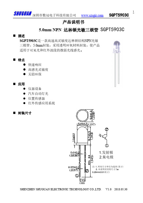
1.发射极2.集电极注: 1. 所有尺寸单位为毫米(英寸) 2. 未说明误差的尺寸为±0.25mm(0.01英寸)产品说明书5.0mm NPN 达林顿光敏三极管SGPT5903C⏹描述SGPT5903C 是一款高速高灵敏度达林顿结构NPN 光敏三极管,5.0mm 封装,采用透明环氧材料封装,使产品适用于可见光和红外波段的微弱光线感光。
⏹特点●快速响应●高感光灵敏度●无铅环保⏹应用●仪器设备●汽车自动灯光●位置传感器●红外传感应用系统⏹封装尺寸⏹极限参数(Ta=25℃)参数名称符号参考值单位集电极-发射极电压V CEO60V发射极-集电极电压V ECO7.0V集电极电流Ic50mA焊接温度*1Tsol260℃工作温度Topr-20~+85℃存储温度Tstg-40~+85℃说明:*1:焊接时间≦5seconds.⏹光电参数(Ta=25℃)参数名称符号最小典型最大单位测试条件频谱范围λ0.5600--1000nm感光峰值波长λP--800--nm集电极–发射极击穿电压BV CEO60----V Ic=100μA,Ee=0mW/cm2发射极-集电极击穿电压BV ECO7.0----V Ic=100μA,Ee=0mW/cm2集电极暗电流I CEO----1000nA V CE=10V,Ee=0mW/cm2集电极-发射极饱和电压V CE(S)--- 1.0V Ic=15mA,Ib=100uA基极-发射极饱和电压V BE(S)--- 1.45V Ic=15mA,Ib=100uA集电极电流I C(on) 2.5 2.8--mA Ev=100Lx,V CE=5V 直流电流放大倍数H FE30000--90000V CE=5V,IC=10mA 上升/下降时间t r/t f--60/60μS V CE=5V,I C=1mAR L=100ΩAmbient Temperature Ta(°C)C o l l e c t o r P o w e rD i s s i p a t i o n (m W )50125020406080100-20-4075100251008060200500Wavelength(nm)R e l a t i v e S p e c t r a l S e n s i t i v i t y (%)Ta=25°4060070080090010001100300Ambient Temperature Ta(°C)R e l a t i v e C o l l e c t o r C u r r e n t (%)40608060100160Vce=5V204080120140Ee=1mW/cm 21020507010Luminance E (Lx )C o l l e c t o r C u r r e n t I c (m A )100100011010101010210Vce=5VT =25 Ca ° 特性曲线图图.1集电极耗散功率与环境温度图.2相对频谱灵敏度图.3相对集电极电流与环境温度图.4集电极电流与辐照度25Ambient Temperature (°C)C o l l e c t o rD a r k C u r r e n t I CE O (n A )50751000Vce=10V 105101010100Collector-Emitter Voltage V CE (V)C o l l e c t o r C u r r e n t I c (m A )12341.02.03.04.05.06.07.0E=10 LxE=50 Lx E=15 LxE=100 LxE=150 Lx 图.5集电极暗电流与环境温度图.6集电极电流与集射电压注意事项:1.我公司保留更改产品材料和以上说明书的权利,更改以上产品说明书恕不另行通知。
爱型电子180667 变速电机电子开关说明书

Eaton 180667Eaton DE11 Variable speed starters, Rated operational voltage 400 V AC, 3-phase, Ie 8.5 A, 4 kW, 5 HP, Radio interference suppression filter DE11-348D5FN-N20NGeneral specificationsEaton DE11 Variable speed starter 1806674015081758326169 mm 230 mm 90 mm 1.6 kgIEC/EN61800-3 IEC/EN61800-5 ULRoHS, ISO 9001Specification for general requirements: IEC/EN 61800-2 UL 508CUL report applies to both US and CanadaCertified by UL for use in Canada CSA-C22.2 No. 14 IEC/EN 61800-3UL Category Control No.: NMMS, NMMS7 CE CULSafety requirements: IEC/EN 61800-5-1 RCMUL File No.: E172143Product NameCatalog Number EANProduct Length/Depth Product Height Product Width Product Weight Certifications Catalog NotesModel CodeParameterization: drivesConnect Parameterization: drivesConnect mobile (App) Parameterization: Fieldbus Parameterization: KeypadRadio interference suppression filterPC connection C3 ≤ 25 m, Radio interference level, maximum motor cable lengthC2 ≤ 10 m, Radio interference level, maximum motor cable lengthCANopen®, built inModbus RTU, built inOP-Bus (RS485), built inIn conjunction with DX-NET-SWD3 SmartWire DT moduleYesIP20NEMA Other1st and 2nd environments (according to EN 61800-3)FS2Variable speed starterFinger and back-of-hand proof, Protection against direct contact (BGV A3, VBG4)MODBUSEtherNet/IPOther bus systemsCANC2, C3: depending on the motor cable length, the connected load, and ambient conditions. External radio interference suppression filters (optional) may be necessary.Optional external radio interference suppression filter for longer motor cable lengths and for use in different EMC environments15 g, Mechanical, According to IEC/EN 60068-2-27, 11 msBranch circuits, (UL/CSA)Features Fitted with:Cable length Communication interface Connection to SmartWire-DT Degree of protection Electromagnetic compatibility Frame sizeProduct category ProtectionProtocolRadio interference classShock resistanceSuitable forResistance: According to EN 61800-5-1Above 1000 m with 1 % derating per 100 mMax. 2000 m-10 °C60 °C-10 °C60 °C-40 °C70 °C< 95 average relative humidity (RH), no condensation, nocorrosion10 A< 3.5 mA (AC-operated)< 10 mA (DC-operated)Maximum of one time every 30 seconds 380 V480 VU/f controlSpeed control with slip compensation 7.6 A8.5 A 8.5 A 7.6 A 5 HP 5 HPVibrationAltitudeAmbient operating temperature - minAmbient operating temperature - maxAmbient operating temperature at 150% overload - minAmbient operating temperature at 150% overload - maxAmbient storage temperature - minAmbient storage temperature - maxClimatic proofingInput current ILN at 150% overload Leakage current at ground IPE - max Mains switch-on frequencyMains voltage - minMains voltage - maxOperating modeOutput frequency - min Assigned motor current IM at 220 - 240 V, 60 Hz, 150% overload Assigned motor current IM at 230 V, 50 Hz, 150% overload Assigned motor current IM at 400 V, 50 Hz, 150% overload Assigned motor current IM at 440 - 480 V, 60 Hz, 150% overload Assigned motor power at 230/240 V, 60 Hz, 1-phaseAssigned motor power at 460/480 V, 60 Hz, 3-phase0 Hz300 Hz400 V AC, 3-phase480 V AC, 3-phase12.75 A10 V DC (Us, max. 0.2 mA)45 Hz66 Hz8.5 A at 150% overload (at an operating frequency of 16 kHz and an ambient air temperature of +50 °C)4 kW400 V AC, 3-phase480 V AC, 3-phase0.03 Hz (Frequency resolution, setpoint value)15 A, UL (Class CC or J), Safety device (fuse or miniature circuit-breaker), Power Wiring200 %, IH, max. starting current (High Overload), For 1.875 seconds every 600 seconds, Power section50/60 Hz16 kHz, 4 - 32 kHz adjustable (audible), fPWM, Power section, Main circuit480 V 5.89 kVA7.07 kVAAdjustable to 100 %, DC - Main circuitMax. 30 % MN, Standard - Main circuit1 (parameterizable, 0 - 10 V DC, 0/4 - 20 mA)4 (parameterizable, 10 - 30 V DC)1 (parameterizable, N/O, 6 A (250 V, AC-1) / 5 A (30 V, DC-1))120 W0 W0 W8.5 A0 WOperation (with 150 % overload)Output frequency - maxOutput voltage (U2)Overload current IL at 150% overloadRated control supply voltageRated frequency - minRated frequency - maxRated operational current (Ie)Rated operational power at 380/400 V, 50 Hz, 3-phase Rated operational voltageResolutionShort-circuit protection ratingStarting current - maxSupply frequencySwitching frequencyVoltage rating - max Apparent power at 400 VApparent power at 480 VBraking torqueNumber of inputs (analog)Number of inputs (digital)Number of outputs (analog)Number of outputs (digital)Number of relay outputsEquipment heat dissipation, current-dependent PvidHeat dissipation capacity PdissHeat dissipation per pole, current-dependent PvidRated operational current for specified heat dissipation (In) Static heat dissipation, non-current-dependent PvsHeat dissipation detailsMeets the product standard's requirements.Meets the product standard's requirements.Meets the product standard's requirements.Meets the product standard's requirements.Meets the product standard's requirements.Does not apply, since the entire switchgear needs to be evaluated.Does not apply, since the entire switchgear needs to be evaluated.Meets the product standard's requirements.Does not apply, since the entire switchgear needs to be evaluated.Meets the product standard's requirements.Does not apply, since the entire switchgear needs to be evaluated.Does not apply, since the entire switchgear needs to be evaluated.Is the panel builder's responsibility.Is the panel builder's responsibility.Is the panel builder's responsibility.Is the panel builder's responsibility.The OP System Bus - Parameterizing - ControlFire modeQuick-Start-Guide DE1 (english)Start, Stopp und BetriebConformal CoatingHow does the internal motor protection work?DX-COM-STICK3_ConnectionUpdate DX-COM-STICK3Electromagnetic compatibility (EMC)Starting, Stopping and OperationSet point settingMotor data Motor Protection V/f curves Slip CompensationI/O ConfigurationConnecting drives to generator suppliesAccess to Parameter Level 2 Parameter Lock Load Default Quick-Start-Guide DE11 (english)HVAC, water/wastewater and industrial mediums - brochure Number 1 in efficiency The easiest way of variable motor speed PowerXL DE1 Variable Speed StarterDA-SW-Codesys 3 SWD for DC1 and DE1DA-SW-USB Driver DX-COM-STICK3-KITDA-SW-drivesConnectDA-SW-drivesConnect - installation helpDA-SW-DE11 CANopen CODESYS2 LibraryDA-SW-DE1 ModbusRTU V1_00 LibraryDA-SW-Codesys 2 SWD for DC1 and DE1DA-SW-drivesConnect - InstallationshilfeDA-SW-DE11 CANopen ConfigFile 203DA-SW-Driver DX-CBL-PC-3M0DA-SW-drivesConnect USB Driver DX-COM-PCKITDA-SW-USB Driver PC Cable DX-CBL-PC-1M5DA-SW-DE11 CANopen CODESYSV3 LibraryDA-SW-DE11 CANopen ConfigFile 210Product Range Catalog Drives Engineering10.2.2 Corrosion resistance10.2.3.1 Verification of thermal stability of enclosures10.2.3.2 Verification of resistance of insulating materials to normal heat10.2.3.3 Resist. of insul. mat. to abnormal heat/fire by internal elect. effects10.2.4 Resistance to ultra-violet (UV) radiation10.2.5 Lifting10.2.6 Mechanical impact10.2.7 Inscriptions10.3 Degree of protection of assemblies10.4 Clearances and creepage distances10.5 Protection against electric shock10.6 Incorporation of switching devices and components10.7 Internal electrical circuits and connections10.8 Connections for external conductors10.9.2 Power-frequency electric strength10.9.3 Impulse withstand voltage Application notes Brochures CataloguesEaton Corporation plc Eaton House30 Pembroke Road Dublin 4, Ireland © 2023 Eaton. All rights reserved. Eaton is a registered trademark.All other trademarks areproperty of their respectiveowners./socialmediaIs the panel builder's responsibility.The panel builder is responsible for the temperature rise calculation. Eaton will provide heat dissipation data for the devices.Is the panel builder's responsibility. The specifications for the switchgear must be observed.Is the panel builder's responsibility. The specifications for the switchgear must be observed.The device meets the requirements, provided the information in the instruction leaflet (IL) is observed.Drives - Product range catalogDA-DC-00004551.pdfDA-DC-00004556.pdfeaton-frequency-inverter-dimensions-010.eps eaton-frequency-inverter-3d-drawing-018.epsDA-CE-ETN.DE11-348D5FN-N20NIL040005ZUPowerXL DE1 variable speed starterMN040003_ENMN040018_ENMN040019_ENMZ040046_ENMN040011_ENDA-CS-de1_fs2_ip20DA-CD-de1_fs2_ip2010.9.4 Testing of enclosures made of insulating material10.10 Temperature rise10.11 Short-circuit rating10.12 Electromagnetic compatibility 10.13 Mechanical function Certification reports DrawingseCAD model Installation instructions Installation videos Manuals and user guidesmCAD model。
HW-D-0.5KVA-NF11应急照明集中电源
安装、使用产品前,请阅读安装使用说明书。
请妥善保管好本手册,以便日后能随时查阅。
HW-D-0.5KV A-NF11应急照明集中电源(消防应急灯具专用应急电源)安装使用说明书(Ver1.05,2020.11)目录1 概述 (1)2 功能 (1)3 技术指标 (1)4 结构特征及配置说明 (1)5 安装与调试 (5)6 操作说明 (8)7 故障、异常信息处理和定期检查 (15)8 报废 (15)9 注意事项 (15)10 产品附件 (15)附录一整机内部接线示意图 (16)I1概述HW-D-0.5KV A-NF11应急照明集中电源(消防应急灯具专用应急电源)(以下简称为HW-D-0.5KV A-NF11)用于消防应急照明疏散指示系统有集中监控要求的控制系统,实现智能疏散系统正常供电和应急供电。
HW-D-0.5KV A-NF11满足GB 17945-2010 《消防应急照明和疏散指示系统》标准中对应急照明集中电源的要求。
2功能2.1给应急照明分配电装置和灯具提供工作电压。
2.2指示灯具当前供电方式。
2.3负载适应能力强,包括电容性、电感性、混合性负载。
2.4过载能力和抗冲击能力强,能承受满负载开机。
2.5具有输入过、欠压,过温,过载、短路等完善的保护功能。
2.6效率高、噪音低、无排烟、无火灾隐患。
2.7自动切换,可实现无人值守。
3技术指标3.1工作电压:主电:交流AC220V/50 Hz,允许变化范围AC187V~AC264V/47 Hz~63Hz;备电:直流DC24V,允许变化范围DC21V~DC27.6V。
3.2输出电压:DC36V3.3额定输出功率:0.5KV A;3.4应急转换效率:>85%;3.5切换时间:0S;3.6最大充电电流:4.5A~5.5A;3.7使用环境工作温度:0℃~+55℃相对湿度≤95%,不凝露3.8外形尺寸:长730mm×宽550mm×厚200mm3.9外壳防护等级:IP303.10输出回路数量:1个3.11配接分配电数量:不超过3个3.12壁挂安装方式,支持侧面进线、背面进线和下进线方式。
AAT 器件选型指南.pdf说明书

Part No.
Amplifiers Include
Vcc (V)
Icc
Ptot
(mA) (mW)
Toper Vio Iio (℃) (mV) (nA)
PKG
Replace Brand
LM358 LM393 LM324 LM339
2
16~32 50
500
0~70
2
2
SOP-8/DIP-8
2
2~36 0.4
128*8 256*8 512*8 1028*8 2056*8 5012*8 10024*8
Frequency Icc
Isb
(KHz)
(mA) (µA)
PKG
Replace Brand
Application
400
0.4~3 0.6~18 SOP-8/DIP-8 ATMEL/ISSI/ST/ROHM
400
400
0.4~3 0.6~18 SOP-8/DIP-8 ATMEL/ISSI/ST/ROHM
400
0.4~3 0.6~18 SOP-8/DIP-8 ATMEL/ISSI/ST/ROHM
400
0.4~3 0.6~18 SOP-8/DIP-8 ATMEL/ISSI/ST/ROHM
■ AAT General Line-up
I2-PAK
TO-220AB
TO-220IS
AAT PRODUCTS FOR CUSTOMERS
General Freque
Vcc
Device
ncy
Name
(KHz)
(V)
Vout (V)
Io (A)
7805
---
5~18
9070T150D1产品数据表说明书

9070T150D1Industrial Control TransformersProduct Description PRODUCT DESCRIPTIONControl power transformers from Schneider Electric set the industry standard for design innovation and performance. They are designed with low impedance windings for excellent voltage regulation, and can accomodate the high inrush current associated with contactors, starters, solenoids, and relays.A variety of designs are available to meet the diverse needs of panel builders and machinery OEMs. The versatility of our control transformer line offers unparalleled options for design engineers. We also have one of the most extensive offering of custom products with no minimum order requirements.We have a national network of distributors to ensure prompt delivery, including industry leading delivery on custom products. In most cases, we can design, manufacture, and ship a custom unit in two weeks or less.The Global Product Offering—Type TType T is our most popular and complete line of control transformers. It comes with unmatched design innovations for top performance and is manufactured using the most advanced insulating materials. The Type T control transformer is the best choice if size and cost are of concern.The Exceptional Regulation Offering —Type EOConstructed with traditional materials and manufacturing processes, Type EO transformers are UL and CSA Component Recognized. Units are designed for 55°C rise. All units are 60HZ rated, withde-rated VA levels for 50HZ.Transformers with Fuse Block Protection—Types TF and EOFWe offer both product lines with factory installed overcurrent protection fuse blocks.Type TF and EOF transformers consist of two primary fuse blocks and one secondary fuse block, a configuration that meets the majority of overcurrent needs by panel builders and machinery OEMs. Since the fuse blocks are pre-wired and mounted on top of the transformer, the Type TF and EOF transformers have the same footprint as the Type T and Type EO units, respectively. This design frees up space normally used for separate fuse blocksWe also have an extensive fuse block offering for custom applications. See the overcurrent section of this catalog for full details.Leaded Control Transformer LineSchneider Electric offers transformers with internally pre-wired 24-inch primary and secondary leads, instead of terminal boards, to make installation easier and faster for many applications. These are only available for single voltage primary and single voltage secondary applications.MultiTapSchneider Electric offers Type T and Type EO transformers in the MultiTap version. The MultiTap control transformer was designed to respond to the increased need for voltage and stock flexibility. It combines multiple primary voltages with one or more secondary voltages, all in a single transfomer. The most flexible MultiTap voltage is the Universal, available on the Type T product line only. It allows for standard primary voltages of 208 to 600V and 110, 115, or 120V secondary voltages.Industrial Control TransformersType T TransformersTYPE T TRANSFORMERSThe Type T units are designed for the global market and are the best choice when size and cost are of concern. This is our most popular and complete offering of industrial control transformers. The following features are included:•50/60 Hz rated•Customer installed accessories (Finger-Safe covers, fuse blocks, fuse clips)•Type T transformers are designed with various temperature classes:—25–150 VA with a 55° C temperature rise, 105° C insulation —200–350 VA with a 80° C temperature rise, 130° C insulation —500–5000 VA with a 115° C temperature rise, 180° C insulationSchneider Electric manufactures a wide variety of voltage combinations for control transformers. The voltage combinations are expressed as “Voltage Codes”, and are embedded within the catalog number of the transformer. Standard codes are listed. If the voltage combination you need is not listed, please call your Schneider Electric distributor for assistance.CE MarkingIndustrial control transformers (ICTs) entering the European Union (EU) after January 1, 1997 are required by EU standards to have CE marking or Declaration of Conformity to CE. EU documentation requires compliance with specification EN 61 558 of the Low Voltage Directive. Type T ICTs from Schneider Electric comply with this specification and are third party tested to T ÜV standards, which adhere to, and are accepted by, EU standards. A Declaration of Conformity for all Type T units is available upon request.Because of different overload criteria in the CE specification,Schneider Elecric dual rates these transformers for UL VA, cUL VA, CSA VA, NOM VA and CE VA ratings (see “Type T VA Ratings” table). Because they are widely used with control circuit panels, ICTs are also required to comply with EN 60 204 and EN 61 558 in these applications. The Type T transformer line complies with EN 60 204 when Fingersafe ® covers are installed.For more information regarding CE marking, please contact your local Schneider Electric field sales office.Type T VA RatingsUL, cUL, CSA and NOM VA RatingCEVA Rating252550507575100100150150200200250160300200350250500300750500100063015001000200015003000200050003000Type T ListingsListingFileVA RangeUL E61239, Guide XPTQ225–5000cUL E612391500–5000CSALR37055, Guide 184-N-9025–1000EN947923, EN 61 558/01.89 (TUV ref: 00941-RAG/sg E9371495E01)25–2009579078, EN 61 558/01.89 (TUV ref: 00941-RAG/sg E9471921E01)250–10009579078, EN 61 558/01.89 (TUV ref: 00941-RAG/sg E9471921.02E01)1500–3000Industrial Control TransformersType T Transformers120 Volt Control SecondaryVoltage and Connection OptionsVoltage CodeVoltagesConnectionsPrimary SecondaryPrimarySecondaryD1220 x 440230 x 460240 x 480110115120220/230/240 V:Connect to H1 and H4Jumper H1 with H3Jumper H2 with H4440/460/480 V:Connect to H1 and H4Jumper H2 with H3Connect to X1 and X2DimensionsVA CatalogNumberFigureAcc. KeyA BCEFSlotsULCEINmmINmmINmmINmmINmmINmm25259070T25D11I 3.0979 3.0076 2.5866 2.0051 2.50640.20 x 0.38 5 x 1050509070T50D11I 3.0979 3.0076 2.5866 2.0051 2.50640.20 x 0.38 5 x 1075759070T75D11I 3.3485 3.3886 2.8973 2.3861 2.81710.20 x 0.48 5 x 121001009070T100D11I 3.3485 3.3886 2.8973 2.3861 2.81710.20 x 0.48 5 x 121501509070T150D11I 3.5991 3.7595 3.2081 2.8873 3.13800.20 x 0.38 5 x 102002009070T200D11I 3.5991 3.7595 3.2081 2.8873 3.13800.20 x 0.38 5 x 102501609070T250D12I 5.30135 3.7595 3.2182 2.8873 3.13800.20 x 0.38 5 x 103002009070T300D12I 4.74120 4.50114 3.8498 2.5665 3.75950.20 x 0.38 5 x 103502509070T350D12I 5.11130 4.50114 3.8498 3.0076 3.75950.20 x 0.38 5 x 105003009070T500D12I 5.49139 4.50114 3.8498 3.5690 3.75950.20 x 0.38 5 x 107505009070T750D12I 5.61143 5.25133 4.51115 3.4387 4.381110.28 x 0.567 x 1410006309070T1000D12I 6.30160 5.25133 4.51115 4.31109 4.381110.28 x 0.567 x 14150010009070T1500D12I 5.921507.06179 6.17157 4.13105 5.811480.28 x 0.567 x 14200015009070T2000D12I 7.171827.06179 6.17157 4.56116 5.811480.28 x 0.567 x 14300020009070T3000D13I 7.241849.002298.75222 4.631187.631940.44 x 1.1311 x 29500030009070T5000D13I9.152329.002298.752226.561677.631940.44 x 1.1311 x 2914T R A N S F O R M E R SIndustrial ControlClass 9070 / Refer to Catalogs 9070CT9901, 7400CT9601Square D ® Type T and MultiTap™ TransformersType T transformers are designed with low impedance windings forexcellent voltage regulation and can accommodate the high inrush current associated with contactors, starters, solenoids, and relays. As the most popular and complete line of control transformers with unmatched design innovations for top performance, Type Ts are manufactured using the most advanced insulating materials and are the best choice if size and cost are of concern. It is available in the MultiTap version, designed to respond to the increased need for voltage and stock flexibility. It combines multiple primary voltages with one or more secondary voltages, all in a single transformer.VAVA Catalog No.$ PriceH W D W e i g h t (l b s )U L /C S A /N O MCEin (mm)in (mm)in (mm)Primary 240 x 480 Secondary 120; Primary 230 x 460 Secondary 115; or Primary 220 x 440Secondary 11025259070T25D174.00 2.58 (65.5) 3.00 (76.2) 3.09 (78.5) 2.550509070T50D177.00 2.58 (65.5) 3.00 (76.2) 3.09 (78.5) 2.575759070T75D192.00 2.89 (73.4) 3.38 (85.8) 3.34 (84.8) 3.81001009070T100D1103.00 2.89 (73.4) 3.38 (85.8) 3.34 (84.8) 3.81501509070T150D1110.00 3.20 (81.3) 3.75 (95.3) 3.59 (91.2) 5.52002009070T200D1136.00 3.20 (81.3) 3.75 (95.3) 3.59 (91.2) 5.52501609070T250D1159.00 3.25 (82.6) 3.75 (95.3) 5.25 (133.4)7.130********T300D1176.00 3.80 (96.5) 4.50 (114.3) 4.70 (119.4)8.53502509070T350D1187.00 3.80 (96.5) 4.50 (114.3) 5.09 (129.3)10.55003009070T500D1233.00 3.80 (96.5) 4.50 (114.3) 5.46 (138.7)11.97505009070T750D1322.00 4.43 (112.5) 5.25 (133.4) 5.66 (143.8)11.010*********T1000D1390.00 4.43 (112.5) 5.25 (133.4) 6.04 (153.4)20.6150010009070T1500D1558.00 6.16 (156.5)7.06 (179.3) 5.81 (147.6)34.0200015009070T2000D1678.00 6.16 (156.5)7.06 (179.3)7.04 (178.8)47.0300020009070T3000D1941.008.46 (214.9)9.00 (228.6) 6.86 (174.2)60.0500030009070T5000D11582.008.46 (214.9)9.00 (228.6)8.73 (221.7)89.0Primary 208 Secondary 12050509070T50D390.00 2.58 (65.5) 3.00 (76.2) 3.09 (78.5) 2.575759070T75D3108.00 2.89 (73.4) 3.38 (85.8) 3.34 (84.8) 3.81001009070T100D3121.00 2.89 (73.4) 3.38 (85.8) 3.34 (84.8) 3.81501509070T150D3153.00 3.20 (81.3) 3.75 (95.3) 3.59 (91.2) 5.52002009070T200D3195.00 3.20 (81.3) 3.75 (95.3) 3.59 (91.2) 5.52501609070T250D3242.00 3.25 (82.6) 3.75 (95.3) 5.25 (133.4)7.130********T300D3248.00 3.80 (96.5) 4.50 (114.3) 4.70 (119.4)8.53502509070T350D3288.00 3.80 (96.5) 4.50 (114.3) 5.09 (129.3)10.55003009070T500D3314.00 3.80 (96.5) 4.50 (114.3) 5.46 (138.7)11.97505009070T750D3443.00 4.43 (112.5) 5.25 (133.4) 5.66 (143.8)11.010*********T1000D3558.00 4.43 (112.5) 5.25 (133.4) 6.04 (153.4)20.6150010009070T1500D3780.00 6.16 (156.5)7.06 (179.3) 5.81 (147.6)34.0200015009070T2000D3905.00 6.16 (156.5)7.06 (179.3)7.04 (178.8)47.0300020009070T3000D31276.008.46 (214.9)9.00 (228.6) 6.86 (174.2)60.0500030009070T5000D32010.008.46 (214.9)9.00 (228.6)8.73 (221.7)89.0Primary 600 Secondary 120; Primary 575 Secondary 115; or Primary 550 Secondary 11050509070T50D590.00 2.58 (65.5) 3 (76.2) 3.09 (78.5) 2.575759070T75D5108.00 2.89 (73.4) 3.38 (85.8) 3.34 (84.8) 3.81001009070T100D5121.00 2.89 (73.4) 3.38 (85.8) 3.34 (84.8) 3.81501509070T150D5153.00 3.20 (81.3) 3.75 (95.3) 3.59 (91.2) 5.52002009070T200D5195.00 3.20 (81.3) 3.75 (95.3) 3.59 (91.2) 5.52501609070T250D5242.00 3.25 (82.6) 3.75 (95.3) 5.25 (133.4)7.130********T300D5248.00 3.80 (96.5) 4.50 (114.3) 4.70 (119.4)8.53502509070T350D5288.00 3.80 (96.5) 4.50 (114.3) 5.09 (129.3)10.55003009070T500D5314.00 3.80 (96.5) 4.50 (114.3) 5.46 (138.7)11.97505009070T750D5443.00 4.43 (112.5) 5.25 (133.4) 5.66 (143.8)11.010*********T1000D5558.00 4.43 (112.5) 5.25 (133.4) 6.04 (153.4)20.6150010009070T1500D5780.00 6.16 (156.5)7.06 (179.3) 5.81 (147.6)34.0200015009070T2000D5905.00 6.16 (156.5)7.06 (179.3)7.04 (178.8)47.0300020009070T3000D51276.008.46 (214.9)9.00 (228.6) 6.86 (174.2)60.0500030009070T5000D52010.008.46 (214.9)9.00 (228.6)8.73 (221.7)89.0Primary 120 Secondary 120; Primary 115 Secondary 115; or Primary 110 Secondary 11050509070T50D24312.00 2.58 (65.5) 3.00 (76.2) 3.09 (78.5) 2.575759070T75D24324.00 2.89 (73.4) 3.38 (85.8) 3.34 (84.8) 3.81001009070T100D24326.00 2.89 (73.4) 3.38 (85.8) 3.34 (84.8) 3.81501509070T150D24348.00 3.20 (81.3) 3.75 (95.3) 3.59 (91.2) 5.52002009070T200D24475.00 3.20 (81.3) 3.75 (95.3) 3.59 (91.2) 5.52501609070T250D24477.00 3.25 (82.6) 3.75 (95.3) 5.25 (133.4)7.130********T300D24481.00 3.8 (96.5) 4.50 (114.3) 4.70 (119.4)8.53502509070T350D24483.00 3.80 (96.5) 4.50 (114.3) 5.09 (129.3)10.55003009070T500D24498.00 3.80 (96.5) 4.50 (114.3) 5.46 (138.7)11.97505009070T750D24560.00 4.43 (112.5) 5.25 (133.4) 5.66 (143.8)11.010*********T1000D24594.00 4.43 (112.5) 5.25 (133.4) 6.04 (153.4)20.6150010009070T1500D24717.00 6.16 (156.5)7.06 (179.3) 5.81 (147.6)34.0200015009070T2000D24929.00 6.16 (156.5)7.06 (179.3)7.04 (178.8)47.0300020009070T3000D241463.008.46 (214.9)9.00 (228.6) 6.86 (174.2)60.0500030009070T5000D242010.008.46 (214.9)9.00 (228.6)8.73 (221.7)89.0Primary 277 Secondary 120Primary 277 Secondary 120 (continued)2002009070T200D4195.00 3.20 (81.3) 3.75 (95.3) 3.59 (91.2) 5.52501609070T250D4242.00 3.25 (82.6) 3.75 (95.3) 5.25 (133.4)7.130********T300D4248.00 3.80 (96.5) 4.50 (114.3) 4.70 (119.4)8.53502509070T350D4288.00 3.80 (96.5) 4.50 (114.3) 5.09 (129.3)10.55003009070T500D4314.00 3.80 (96.5) 4.50 (114.3) 5.46 (138.7)11.97505009070T750D4443.00 4.43 (112.5) 5.25 (133.4) 5.66 (143.8)11.010*********T1000D4558.00 4.43 (112.5) 5.25 (133.4) 6.04 (153.4)20.6150010009070T1500D4780.00 6.16 (156.5)7.06 (179.3) 5.81 (147.6)34.0200015009070T2000D4905.00 6.16 (156.5)7.06 (179.3)7.04 (178.8)47.0300020009070T3000D41276.008.46 (214.9)9.00 (228.6) 6.86 (174.2)60.0500030009070T5000D42010.008.46 (214.9)9.00 (228.6)8.73 (221.7)89.0VA VA Catalog No.$ PriceHW D W e i g h t (l b s )U L /C S A /N O MCEin (mm)in (mmin (mm)Primary 240 x 480 Secondary 120/240; Primary 230 x 460 Secondary 115/230; orPrimary 220 x 440 Secondary 110/22050509070T50D31125.00 2.58 (65.5) 3.00 (76.2) 3.09 (78.5) 2.575759070T75D31131.00 2.89 (73.4) 3.38 (85.8) 3.34 (84.8) 3.81001009070T100D31138.00 2.89 (73.4) 3.38 (85.8) 3.34 (84.8) 3.81501509070T150D31182.00 3.20 (81.3) 3.75 (95.3) 3.59 (91.2) 5.52002009070T200D31235.00 3.20 (81.3) 3.75 (95.3) 3.59 (91.2) 5.52501609070T250D31248.00 3.25 (82.6) 3.75 (95.3) 5.25 (133.4)7.130********T300D31290.00 3.80 (96.5) 4.50 (114.3) 4.70 (119.4)8.53502509070T350D31303.00 3.80 (96.5) 4.50 (114.3) 5.09 (129.3)10.55003009070T500D31339.00 3.80 (96.5) 4.50 (114.3) 5.46 (138.7)11.97505009070T750D31473.00 4.43 (112.5) 5.25 (133.4) 5.66 (143.8)11.010*********T1000D31558.00 4.43 (112.5) 5.25 (133.4) 6.04 (153.4)20.6150010009070T1500D31816.00 6.16 (156.5)7.06 (179.3) 5.81 (147.6)34.0200015009070T2000D31905.00 6.16 (156.5)7.06 (179.3)7.04 (178.8)47.0300020009070T3000D311486.008.46 (214.9)9.00 (228.6) 6.86 (174.2)60.0500030009070T5000D312010.008.46 (214.9)9.00 (228.6)8.73 (221.7)89.0Primary 120 x240 Secondary 120/240; Primary 115 x 230 Secondary 115/230; orPrimary 110 x 2200 Secondary 110/22050509070T50D55312.00 2.58 (65.5) 3.00 (76.2) 3.09 (78.5) 2.575759070T75D55324.00 2.89 (73.4) 3.38 (85.8) 3.34 (84.8) 3.81001009070T100D55326.00 2.89 (73.4) 3.38 (85.8) 3.34 (84.8) 3.81501509070T150D55348.00 3.20 (81.3) 3.75 (95.3) 3.59 (91.2) 5.52002009070T200D55475.00 3.20 (81.3) 3.75 (95.3) 3.59 (91.2) 5.52501609070T250D55477.00 3.25 (82.6) 3.75 (95.3) 5.25 (133.4)7.130********T300D55481.00 3.80 (96.5) 4.50 (114.3) 4.70 (119.4)8.53502509070T350D55483.00 3.80 (96.5) 4.50(114.3) 5.09 (129.3)10.55003009070T500D55498.00 3.80 (96.5) 4.50 (114.3) 5.46 (138.7)11.97505009070T750D55560.00 4.43 (112.5) 5.25 (133.4) 5.66 (143.8)11.010*********T1000D55594.00 4.43 (112.5) 5.25 (133.4) 6.04 (153.4)20.6150010009070T1500D55856.00 6.16 (156.5)7.06 (179.3) 5.81 (147.6)34.0200015009070T2000D55929.00 6.16 (156.5)7.06 (179.3)7.04 (178.8)47.0300020009070T3000D551588.008.46 (214.9)9.00 (228.6) 6.86 (174.2)60.0500030009070T5000D552010.008.46 (214.9)9.00 (228.6)8.73 (221.7)89.0Primary 240 X 480 Secondary 24/120 (24 V limited to 20% Capacity)50509070T50D1590.00 2.58 (65.5) 3.00 (76.2) 3.09 (78.5) 2.575759070T75D15108.00 2.89 (73.4) 3.38 (85.8) 3.34 (84.8) 3.81001009070T100D15138.00 2.89 (73.4) 3.38 (85.8) 3.34 (84.8) 3.81501509070T150D15153.00 3.20 (81.3) 3.75 (95.3) 3.59 (91.2) 5.52002009070T200D15195.00 3.2 0(81.3) 3.75 (95.3) 3.59 (91.2) 5.52501609070T250D15248.00 3.25 (82.6) 3.75 (95.3) 5.25 (133.4)7.130********T300D15290.00 3.80 (96.5) 4.50 9114.3) 4.70 (119.4)8.53502509070T350D15303.00 3.80 (96.5) 4.50 (114.3) 5.09 (129.3)10.55003009070T500D15339.00 3.80 (96.5) 4.50 (114.3) 5.46 (138.7)11.97505009070T750D15473.00 4.43 (112.5) 5.25 (133.4) 5.66 (143.8)11.010*********T1000D15558.00 4.43 (112.5) 5.25 (133.4) 6.04 (153.4)20.6150010009070T1500D15816.00 6.16 (156.5)7.06 (179.3) 5.81 (147.6)34.0200015009070T2000D15905.00 6.16 (156.5)7.06 (179.3)7.04 (178.8)47.0300020009070T3000D151486.008.46 (214.9)9.00 (228.6) 6.86 (174.2)60.0500030009070T5000D152010.008.46 (214.9)9.00 (228.6)8.73 (221.7)89.0Primary 480 Secondary 24050509070T50D1290.00 2.58 (65.5) 3.00 (76.2) 3.09 (78.5) 2.575759070T75D12324.00 2.89 (73.4) 3.38 (85.8) 3.34 (84.8) 3.81001009070T100D12121.00 2.89 (73.4) 3.38 (85.8) 3.34 (84.8) 3.81501509070T150D12153.00 3.20 (81.3) 3.75 (95.3) 3.59 (91.2) 5.52002009070T200D12195.00 3.20 (81.3) 3.75 (95.3) 3.59 (91.20) 5.52501609070T250D12242.00 3.25 (82.6) 3.75 (95.3) 5.25 (133.4)7.130********T300D12248.00 3.80 (96.5) 4.50 (114.3) 4.70 (119.4)8.53502509070T350D12288.00 3.80 (96.5) 4.50 (114.3) 5.09 (129.3)10.55003009070T500D12314.00 3.80 (96.5) 4.50 (114.3) 5.46 (138.7)11.97505009070T750D12443.00 4.43 (112.5) 5.25 (133.4) 5.66 (143.8)11.010*********T1000D12558.00 4.43 (112.5) 5.25 (133.4) 6.04 (153.4)20.6150010009070T1500D12780.00 6.16 (156.5)7.06 (179.3) 5.81 (147.6)34.0200015009070T2000D12905.00 6.16 (156.5)7.06 (179.3)7.04 (178.8)47.0VA VA Catalog No.$ PriceH W DW e i g h t (l b s )U L /C S A /N O MCEin (mm)in (mm)in (mm)9070T150D1。
Z-15GW3-B中文资料(omron)中文数据手册「EasyDatasheet - 矽搜」

• 这些交换机使用一个橡胶套管上情况之间致动器和粘合剂填充和 覆盖,以增加耐滴水.
• 模型与防滴端子防护护盖并用树脂充填模终端也可提供.
分割接触模型
• 这种类型是在结构上不同之处在于它具有两对同时演技触点通过拆 分移动触点通用基本开关相同.
• 由于移动触点被连接到一公共端,并联或串联连接是可能.
2.接 触 间 隙 F:1毫米(大容量)
3.执 行 器
无:引脚柱塞
S: 超薄弹簧柱塞 D: 短弹簧柱塞 Q: 面板安装柱塞 Q22:面板安装滚轮柱塞 W: 铰链杠杆 W22:短铰链滚轮摇臂 W2:铰链滚轮摇臂 M22:反向短铰链滚轮摇臂
4.施 工 Y:
分体式接触式
5.终 端
无:焊接端子
B: 螺丝端子
芯片中文手册,看全文,戳
防滴型号
执行器 引脚柱塞 短弹簧柱塞
弹簧柱塞
面板安装柱塞 面板安装滚轮 柱塞 面板安装交叉 滚轮柱塞 钢板弹簧
滚轮钢板弹簧 短铰链杆 长铰链杆 铰链杠杆 短铰链滚轮摇臂 铰链滚轮摇臂 单向短 铰链滚轮摇臂
反向铰链杠杆* 2
反向短铰链
滚轮摇臂* 2
反向铰链滚轮
• 如果模型被用作双触点开关高度可靠微负载切换得到防护证.
防护持接触模型
• 所维护接触型具有在开关壳体底部有一个复位键,除位于复位按钮 相对侧上按键(柱塞).使用这些按钮交替进行.
• 由于该开关具有比超程更大预行程,很适合 在正反转控制电路中使用,手动复位电路,安全 限制电路,以及其它电路这是不优选 自动复位. (有关详细信息,请参照各 数据表.)
---
---
---
---
---
---
---
---
PMC150, PMS150 datasheet V005_CN
PMC150/PMS150 系列
8 位 IO 类型单片机
重要声明
应广科技保留权利在任何时候变更或终止产品,建议客户在使用或下单前与应广科技或代理商 联系以取得最新、最正确的产品信息。
应广科技不担保本产品适用于保障生命安全或紧急安全的应用,应广科技不为此类应用产品承 担任何责任。关键应用产品包括,但不仅限于,可能涉及的潜在风险的死亡,人身伤害,火灾或严 重财产损失。
2. 系统概述和方框图 ................................................................................................................................. 7 3. 引脚功能说明 ........................................................................................................................................ 8
4. 器件电气特性 ...................................................................................................................................... 10 4.1 直流交流电气特性 ........................................................................................................................ 10 4.2 绝对最大值 ................................................................................................................................... 11 4.3 IHRC 频率与 VDD 关系曲线图 .................................................................................................... 12 4.4 ILRC 频率与 VDD 关系曲线图..................................................................................................... 12 4.5 IHRC 频率与温度关系曲线图 ...................................................................................................... 13 4.6 工作电流与 VDD、系统时钟 CLK=IHRC/n 曲线图 ....................................................................... 13 4.7 工作电流与 VDD、系统时钟 CLK=ILRC/n 曲线图........................................................................ 14 4.8 最低工作电流与 VDD、系统时钟 CLK=ILRC/n 曲线图 ................................................................ 15 4.9 引脚拉高电阻曲线图..................................................................................................................... 15 4.10 引脚输出驱电流(Ioh)与灌电流(Iol) 曲线图 ................................................................................. 16 4.11 引脚输出输入高电压与低电压(VIH / VIL) 曲线图 ......................................................................... 16
斐雪派克黑色电磁灶安装指南说明书
建议你把每台产品安装在不同开孔内,相邻玻璃面板之间的最小距离为5mm。如果在同一个开孔内并排安装 多台产品,需要使用单独的连接带套件。延长接头可向最近的斐雪派克授权服务中心购买,也可以访问公司 网站购买。 如果并排安装多台不同的产品(例如在一台电磁灶旁边安装一台铁锅灶头),不同产品的最小间隙要求可能 不相同,始终要满足较大的距离要求。
轴测图
FRONT
D
H
F
I
P剖RO视FI图LE
产品尺寸
A 炉灶总高度 B 炉灶总宽度 C 炉灶总深度 D 背板高度 E 背板宽度 F 背板深度 G 炉灶玻璃面板高度* H 炉灶玻璃面板前面突出深度** I 炉灶玻璃面板后面突出深度 J 炉灶玻璃面板侧面突出深度
图中所示为CI603DTB型炉灶。 * 包括凸缘和双面胶 ** 包括前镶边条
安全警告
阅读并妥善保存本指南
通用
z 在安装此产品之前仔细阅读本说明书。 z 妥善保存本说明书供当地电气检查员之用。 z 必须按照当地建筑法规和电气法规要求进行安装。 z 此电器只能由接受过斐雪派克专业培训和支持的维修技术员或资深电工安装和维修。 z 制造商对电器安装不当造成的损坏不承担任何责任。安装不当可能会造成人身伤害或财物损失,保修或责
最大2 最大10
独立安装
A
B 俯视图
开孔尺寸
A 开孔总宽度 B 开孔总深度 C 开孔转角半径
正视图
开孔尺寸 — 760MM型
BF C
CI764DTB MM 725 490
最大10
开孔尺寸
A 刨槽总宽度 B 刨槽总深度 C 补偿突出余量 D 刨槽高度 E 开孔宽度 F 开孔深度 G 刨槽转角半径 H 开孔转角半径
黑色电磁灶
SMAZ5V1 - SMAZ39 1.0W 表面载入抗干扰电容器数据手册说明书
Features∙ 1.0W Power Dissipation∙ Ideally Suited for Automated Assembly ∙ 5.1V - 39V Nominal Zener Voltage Range ∙ Standard V Z Tolerance is ± 5%∙ Lead Free Finish; RoHS Compliant (Notes 1 & 2) ∙Halogen and Antimony Free. “Green” Device (Note 3)Mechanical Data∙ Case: SMA∙ Case Material: Molded Plastic. UL Flammability Classification Rating 94V-0∙ Moisture Sensitivity: Level 1 per J-STD-020∙ Terminals: Lead Free Plating (Matte Tin Finish). Solderable per MIL-STD-202, Method 208∙ Polarity: Cathode Notch or Cathode Band ∙Weight: 0.064 grams (Approximate)Ordering Information (Note 4)*x = Device Voltage, e.g., SMAZ5V1-13-F. Notes:1. EU Directive 2002/95/EC (RoHS) & 2011/65/EU (RoHS 2) compliant. All applicable RoHS exemptions applied.2. See /quality/lead_free.html for more information about Diodes Incorporate d’s definitions of Halogen - and Antimony-free, "Green" and Lead-free.3. Halogen- and Antimony-free "Green” products are defined as those which contain <900ppm bromine, <900ppm chlorine (<1500ppm total Br + Cl) and <1000ppm antimony compounds.4. For packaging details, go to our website at /products/packages.html.Marking InformationTop ViewBottom ViewGreenxxx = Product Type Marking Code (See Electric Characteristics Table) = Manufacturers’ Code Marking YWW = Date Code MarkingY = Last Digit of Year (ex: 6 for 2016) WW = Week Code (01 to 53)Maximum Ratings(@T A = +25°C, unless otherwise specified.)Thermal CharacteristicsNotes: 5. Device mounted on FR-4 PCB, 1 inch x 0.85 inch x 0.062 inch; pad layout as shown on Diodes Inc.’s package outlines page, which can be found on our website at /package-outlines.html.6. Short duration pulse test used to minimize self-heating effect.0.20.40.60.81.01.250175P P O W E R D I S S I P A T I O N (W )D T , AMBIENT TEMPERATURE (C)A ︒Fig. 1 Power Dissipation vs. Ambient Temperature101001,000C , T O T A L C A P A C I T A N C E (p F )T V , REVERSE VOLTAGE (V)Fig. 2 Typical T otal Capacitance vs. Reverse Voltage R0.11102000.5 1.0 1.5 2.0 2.5I , P E A K F O R W A R D C U R R E N T (A )F M V , PEAK FORWARD VOLTAGE (V)Fig. 3 Peak Forward Current vs. Peak Forward Voltage FM0.0010.010.11101001,0002,000V , ZENER REGULATION VOLTAGE (V)ZT Fig. 4 Leakage Current vs. Regulation Voltage101001,000110V , ZENER REGULATION VOLTAGE (V)ZTPackage Outline DimensionsPlease see /package-outlines.html for the latest version.SMASuggested Pad LayoutPlease see /package-outlines.html for the latest version.SMA。
74ALVC373BQ,115,74ALVC373PW,118,74ALVC373D,112,74ALVC373PW,112, 规格书,Datasheet 资料
74ALVC373Octal D-type transparent latch; 3-stateRev. 02 — 18 October 2007Product data sheet1.General descriptionThe 74ALVC373 is an octal D-type transparent latch featuring separate D-type inputs foreach latch and3-state true outputs for bus-oriented applications.A latch enable(LE)inputand an outputs enable (OE) input are common to all latches.When pin LE is HIGH, data at the D-inputs (pins D0 to D7) enters the latches. In thiscondition, the latches are transparent, that is, a latch output will change each time itscorresponding D-input changes. When pin LE is LOW, the latches store the informationthat was present at the D-inputs one set-up time preceding the HIGH-to-LOW transition ofpin LE.When pin OE is LOW,the contents of the eight latches are available at the Q-outputs(pinsQ0 to Q7). When pin OE is HIGH, the outputs go to the high-impedance OFF-state.Operation of input pin OE does not affect the state of the latches.The 74ALVC373 is functionally identical to the 74ALVC573, but has a different pinarrangement.2.Featuress Wide supply voltage range from 1.65V to3.6Vs 3.6V tolerant inputs/outputss CMOS low power consumptions Direct interface with TTL levels (2.7V to 3.6V)s Power-down modes Latch-up performance exceeds 250mAs Complies with JEDEC standards:x JESD8-7 (1.65V to 1.95V)x JESD8-5 (2.3V to 2.7V)x JESD8B/JESD36 (2.7V to 3.6V)s ESD protection:x HBM JESD22-A114E exceeds 2000Vx MM JESD22-A115-A exceeds 200V3.Ordering information4.Functional diagramTable 1.Ordering informationType numberPackageTemperature range NameDescriptionVersion 74ALVC373D−40°C to +85°CSO20plastic small outline package; 20leads;body width 7.5mmSOT163-174ALVC373PW −40°C to +85°C TSSOP20plastic thin shrink small outline package; 20leads;body width 4.4mmSOT360-174ALVC373BQ−40°C to +85°CDHVQFN20plastic dual in-line compatible thermal enhanced verythin quad flat package; no leads; 20terminals;body 2.5×4.5×0.85mmSOT764-1Fig 1.Logic symbol Fig 2.IEC logic symbolmna881D0D1D2D3D4D5D6D7Q0Q1Q2Q3Q4Q5Q6Q7LE 111181714138743191615129652OE mna880191615129651EN 11C11D2181714138743Fig 3.Functional diagrammna8823-STATE OUTPUTSLATCH 1 to 8Q0Q1Q2Q3Q4Q5Q6Q7191615129652D0D1D2D3D4D5D6D7LE OE1811117 14138743Fig 4.Logic diagram (one latch)Fig 5.Logic diagramQLEDLELELEmna189mna883Q4D4D LE Q Q3D3D LE Q Q2D2D LE Q Q1D1D LE LE LE Q Q0D0D Q LE OELE LE LE LE Q5D5D LE Q LE Q6D6D LE Q LE Q7D7D LEQLE5.Pinning information5.1Pinning5.2Pin description(1)The die substrate is attached to this pad usingconductive die attach material.It can not be used as a supply pin or input.Fig 6.Pin configuration SO20 and TSSOP20Fig 7.Pin configuration DHVQFN20373AOE V CC Q0Q7D0D7D1D6Q1Q6Q2Q5D2D5D3D4Q3Q4GND LE001aad0901234567891012111413161518172019001aad089373ATransparent top viewQ4D3Q3D4D2D5Q2Q5Q1Q6D1D6D0D7Q0Q7G N D L E O EV C C912813714615GND (1)5164173182191011120terminal 1index areaTable 2.Pin descriptionSymbol PinDescription D[0:7]3, 4, 7, 8, 13, 14, 17, 18data inputLE 11latch enable input (active HIGH)OE 1output enable input (active LOW)Q[0:7]2, 5, 6, 9, 12, 15, 16, 193-state latch output V CC 20supply voltage GND10ground (0V)6.Functional description[1]H = HIGH voltage levelh = HIGH voltage level one set-up time prior to the HIGH-to-LOW LE transition L = LOW voltage levell = LOW voltage level one set-up time prior to the HIGH-to-LOW LE transition X = don’t careZ = High-impedance OFF-state7.Limiting values[1]The input and output voltage ratings may be exceeded if the input and output current ratings are observed.[2]When V CC = 0 V (power-down mode), the output voltage can be 3.6V in normal operation.[3]For SO20 packages: above 70°C derate linearly with 8mW/K.For TSSOP20 packages: above 60°C derate linearly with 5.5mW/K.For DHVQFN20 packages: above 60°C derate linearly with 4.5mW/K.Table 3.Functional table [1]Operating modes Input Internal latchOutput OELE Dn Qn Enable and read register (transparent mode)L H L L L L H H H H Latch and read register L L l L L L L h H H Latch register and disable outputsH X X X Z HLhHZTable 4.Limiting valuesIn accordance with the Absolute Maximum Rating System (IEC 60134). Voltages are referenced to GND (ground =0V).Symbol Parameter Conditions Min Max Unit V CC supply voltage −0.5+4.6V I IK input clamping current V I <0V−50-mA V I input voltage−0.5+4.6V I OK output clamping current V O >V CC or V O <0V -±50mA V Ooutput voltageoutput HIGH or LOW state [1][2]−0.5V CC +0.5V output 3-state−0.5+4.6V power-down mode, V CC = 0V[2]−0.5+4.6V I O output current V O =0V to V CC-±50mA I CC supply current -100mA I GND ground current −100-mA T stg storage temperature −65+150°C P tottotal power dissipationT amb =−40°C to +85°C[3]-500mW8.Recommended operating conditionsTable 5.Recommended operating conditionsSymbol Parameter Conditions Min Max UnitV CC supply voltage 1.65 3.6VV I input voltage0 3.6VV O output voltage output HIGH or LOW state0V CC Voutput 3-state0 3.6Vpower-down mode; V CC=0V0 3.6VT amb ambient temperature in free air−40+85°C∆t/∆V input transition rise and fall rate V CC=1.65V to2.7V-20ns/VV CC=2.7V to3.6V-10ns/V 9.Static characteristicsTable 6.Static characteristicsAt recommended operating conditions. Voltages are referenced to GND (ground = 0 V).Symbol Parameter Conditions−40°C to +85°C UnitMin Typ[1]MaxV IH HIGH-level input voltage V CC = 1.65 V to 1.95 V0.65× V CC--VV CC = 2.3 V to 2.7 V 1.7--VV CC = 2.7 V to 3.6 V 2.0--VV IL LOW-level input voltage V CC = 1.65 V to 1.95 V--0.35× V CC VV CC = 2.3 V to 2.7 V--0.7VV CC = 2.7 V to 3.6 V--0.8VV OH HIGH-level output voltage V I=V IH or V ILI O=−100µA; V CC=1.65V to3.6V V CC−0.2--VI O=−6mA; V CC = 1.65 V 1.25 1.51-VI O=−12mA; V CC = 2.3V 1.8 2.10-VI O=−18mA; V CC = 2.3V 1.7 2.01-VI O=−12mA; V CC = 2.7 V 2.2 2.53-VI O=−18mA; V CC = 3.0 V 2.4 2.76-VI O=−24mA; V CC = 3.0 V 2.2 2.68-VV OL LOW-level output voltage V I=V IH or V ILI O=100µA; V CC=1.65V to3.6 V--0.2VI O=6mA; V CC = 1.65 V-0.110.3VI O=12mA; V CC = 2.3V-0.170.4VI O=18mA; V CC = 2.3V-0.250.6VI O=12mA; V CC = 2.7 V-0.160.4VI O=18mA; V CC = 3.0V-0.230.4VI O=24mA; V CC = 3.0 V-0.300.55VI I input leakage current V CC = 3.6 V; V I=3.6V or GND-±0.1±5µA[1]All typical values are measured at V CC =3.3V (unless stated otherwise) and T amb =25°C.10.Dynamic characteristicsI OZ OFF-state output current V I =V IH or V IL ; V CC =1.65V to 3.6V;V O =3.6V or GND;-±0.1±10µA I OFF power-off leakage supply V CC = 0 V; V I or V O = 0V to 3.6V -±0.1±10µA I CC supply currentV CC = 3.6 V; V I =V CC or GND;I O =0A-0.210µA ∆I CC additional supply current per input pin; V CC =3.0V to 3.6 V;V I =V CC −0.6V; I O =0A-5750µA C Iinput capacitance-3.5-pFTable 6.Static characteristics …continuedAt recommended operating conditions. Voltages are referenced to GND (ground = 0 V).Symbol Parameter Conditions−40°C to +85°CUnit MinTyp [1]Max Table 7.Dynamic characteristicsVoltages are referenced to GND (ground =0V). For test circuit see Figure 12.Symbol Parameter Conditions−40°C to +85°C UnitMin Typ [1]Max t pdpropagation delayDn to Qn; see Figure 8[2]V CC = 1.65 V to 1.95 V 1.0 2.5 5.4ns V CC = 2.3V to 2.7V 1.0 2.0 3.5ns V CC = 2.7 V 1.0 2.3 3.6ns V CC = 3.0 V to 3.6 V 1.0 2.2 3.3ns LE to Qn; see Figure 9V CC = 1.65 V to 1.95 V 1.0 2.8 6.0ns V CC = 2.3V to 2.7V 1.0 2.1 3.8ns V CC = 2.7 V 1.0 2.4 3.7ns V CC = 3.0 V to 3.6 V1.02.33.3ns t enenable timeOE to Qn; see Figure 10[2]V CC = 1.65 V to 1.95 V 1.5 3.0 6.4ns V CC = 2.3V to 2.7V 1.0 2.4 4.5ns V CC = 2.7 V 1.5 3.0 4.6ns V CC = 3.0 V to 3.6 V1.02.3 4.0ns t disdisable timeOE to Qn; see Figure 10[2]V CC = 1.65 V to 1.95 V 1.5 3.47.0ns V CC = 2.3V to 2.7V 1.0 2.2 4.4ns V CC = 2.7 V 1.5 2.8 4.4ns V CC = 3.0 V to 3.6 V1.02.74.4ns[1]Typical values are measured at T amb =25°C [2]t pd is the same as t PHL and t PLH .t en is the same as t PZH and t PZL .t dis is the same as t PHZ and t PLZ .[3]C PD is used to determine the dynamic power dissipation (P D in µW).P D =C PD ×V CC 2×f i ×N +Σ(C L ×V CC 2×f o )where:f i = input frequency in MHz; f o =output frequency in MHz C L =output load capacitance in pF V CC =supply voltage in Volts N =number of inputs switchingΣ(C L ×V CC 2×f o )=sum of the outputst Wpulse widthLE pulse width HIGH; see Figure 9V CC = 1.65 V to 1.95 V 3.8 1.0-ns V CC = 2.3V to 2.7V 3.30.8-ns V CC = 2.7 V 3.3 2.0-ns V CC = 3.0 V to 3.6 V3.3 2.2-ns t suset-up timeDn to LE; see Figure 11V CC = 1.65 V to 1.95 V 0.80.1-ns V CC = 2.3V to 2.7V 0.80.1-ns V CC = 2.7 V 0.80.1-ns V CC = 3.0 V to 3.6 V0.80.1-ns t hhold timeDn to LE; see Figure 11V CC = 1.65 V to 1.95 V 0.8−0.1-ns V CC = 2.3V to 2.7V 0.8−0.2-ns V CC = 2.7 V 0.8−0.3-ns V CC = 3.0 V to 3.6 V0.7−0.1-ns C PDpower dissipation capacitanceper latch; V I = GND to V CC ; V CC = 3.3V [3]outputs HIGH or LOW state -35-pF outputs 3-state-14-pFTable 7.Dynamic characteristics …continuedVoltages are referenced to GND (ground =0V). For test circuit see Figure 12.Symbol Parameter Conditions−40°C to +85°C UnitMin Typ [1]Max11.WaveformsMeasurement points are given in Table 8.V OL and V OH are the typical output voltage levels that occur with the output load.Fig 8.Input Dn to output Qn propagation delay times mna884Dn inputQn outputt PHLt PLHGNDV IV MV MV OHV OLTable 8.Measurement pointsSupply voltage V CCV M Output V xV y1.65V to 1.95V 0.5V CC V OL + 0.15V V OH − 0.15V2.3V to 2.7V 0.5V CC V OL + 0.15V V OH − 0.15V 2.7V 1.5 V V OL + 0.3V V OH − 0.3V3.0V to 3.6V1.5 VV OL + 0.3VV OH − 0.3VMeasurement points are given in Table 8.V OL and V OH are the typical output voltage levels that occur with the output load.Fig tch enable (LE) pulse width and latch enable input to output (Qn) propagation delaysmna885LE inputQn outputt PHLt PLHt W V MV OHV IGNDV OLV MMeasurement points are given in Table 8.V OL and V OH are the typical output voltage levels that occur with the output load.Fig 10.Enable and disable timesmna395t PLZt PHZoutputs disabledoutputs enabledV YV Xoutputs enabledQ n output LOW-to-OFF OFF-to-LOWQ n output HIGH-to-OFF OFF-to-HIGHOE inputV IV OLV OHV CCV MGNDGNDt PZLt PZHV MV MMeasurement points are given in Table 8.The shaded areas indicate when the input is permitted to change for predicable output performance.Fig 11.The data set-up and hold times for Dn input to LE inputmna887t ht sut ht suV MV MV IGNDV IGNDLE inputDn inputTest data is given in T able 9.Definitions for test circuit:R L = Load resistance.C L = Load capacitance including jig and probe capacitance.R T = Termination resistance should be equal to output impedance Z o of the pulse generator.V EXT = External voltage for measuring switching times.Fig 12.Test circuitry for switching times V M V Mt Wt W10 %90 %0 VV IV I negative pulsepositive pulse0 VV MV M90 %10 %t ft r t rt f 001aae331V EXTV CCV I V ODUTC LR TR LR LGTable 9.Test dataSupply voltageInput Load V EXT V It r , t f C L R L t PLH , t PHL t PLZ , t PZL t PHZ , t PZH 1.65V to 1.95V V CC ≤ 2.0 ns 30pF 1 k Ωopen 2× V CC GND 2.3V to 2.7V V CC ≤ 2.0 ns 30pF 500Ωopen 2× V CC GND 2.7V 2.7V ≤ 2.5ns 50pF 500Ωopen 6 V GND 3.0V to 3.6V2.7V≤ 2.5ns50pF500Ωopen6 VGND12.Package outlineFig 13.Package outline SOT163-1 (SO20)UNIT A max.A 1A 2A 3b p c D (1)E (1)(1)e H E L L p Q Zy w v θREFERENCESOUTLINEVERSION EUROPEAN PROJECTIONISSUE DATE IEC JEDEC JEITAmm inches 2.650.30.12.452.250.490.360.320.2313.012.67.67.4 1.2710.6510.001.11.00.90.48oo 0.250.1DIMENSIONS (inch dimensions are derived from the original mm dimensions)Note1. Plastic or metal protrusions of 0.15 mm (0.006 inch) maximum per side are not included.1.10.4SOT163-11020w Mb pdetail XZ e111D y0.25 075E04MS-013pin 1 index0.10.0120.0040.0960.0890.0190.0140.0130.0090.510.490.300.290.051.40.0550.4190.3940.0430.0390.0350.0160.010.250.010.0040.0430.0160.010510 mmscaleXθAA 1A 2H EL p QE cLv M A(A )3ASO20: plastic small outline package; 20 leads; body width 7.5 mmSOT163-199-12-2703-02-19Fig 14.Package outline SOT360-1 (TSSOP20)UNIT A 1A 2A 3b p c D (1)E (2)(1)e H E L L p Q Z y w v θ REFERENCESOUTLINE VERSION EUROPEAN PROJECTIONISSUE DATE IECJEDEC JEITAmm0.150.050.950.800.300.190.20.16.66.44.54.30.656.66.20.40.30.50.280oo 0.130.10.21DIMENSIONS (mm are the original dimensions)Notes1. Plastic or metal protrusions of 0.15 mm maximum per side are not included.2. Plastic interlead protrusions of 0.25 mm maximum per side are not included.0.750.50SOT360-1MO-15399-12-2703-02-19w Mb pD Ze0.251102011pin 1 indexθAA 1A 2L p Qdetail XL(A )3H EE cv M AXAy0 2.5 5 mmscaleTSSOP20: plastic thin shrink small outline package; 20 leads; body width 4.4 mm SOT360-1Amax.1.1Fig 15.Package outline SOT764-1 (DHVQFN20)terminal 1index area0.51A 1E h b UNIT y e 0.2c REFERENCESOUTLINE VERSION EUROPEAN PROJECTIONISSUE DATE IEC JEDEC JEITA mm 4.64.4D h 3.152.85y 12.62.41.150.85e 13.50.300.180.050.000.050.1DIMENSIONS (mm are the original dimensions) SOT764-1MO-241- - -- - -0.50.3L 0.1v 0.05w 02.5 5 mmscaleSOT764-1DHVQFN20: plastic dual in-line compatible thermal enhanced very thin quad flat package; no leads;20 terminals; body 2.5 x 4.5 x 0.85 mmA (1)max.AA 1cdetail Xyy 1Ce LE hD he e 1b2919121110120XD EC B Aterminal 1index areaA C CB v M w M E (1)Note1. Plastic or metal protrusions of 0.075 mm maximum per side are not included.D (1)02-10-1703-01-2713.Abbreviations14.Revision historyTable 10.AbbreviationsAcronym DescriptionCDM Charged Device Model DUT Device Under Test ESD ElectroStatic Discharge HBM Human Body Model MM Machine ModelTTLT ransistor-Transistor LogicTable 11.Revision historyDocument ID Release date Data sheet status Change notice Supersedes 74ALVC373_220071018Product data sheet-74ALVC373_1Modifications:•The format of this data sheet has been redesigned to comply with the new identity guidelines of NXP Semiconductors.•Legal texts have been adapted to the new company name where appropriate.•Section 3: DHVQFN20 package added.•Section 7: derating values added for DHVQFN20 package.•Section 12: outline drawing added for DHVQFN20 package.74ALVC373_120020226Product specification--15.Legal information15.1Data sheet status[1]Please consult the most recently issued document before initiating or completing a design.[2]The term ‘short data sheet’ is explained in section “Definitions”.[3]The product status of device(s)described in this document may have changed since this document was published and may differ in case of multiple devices.The latest product status information is available on the Internet at URL .15.2DefinitionsDraft —The document is a draft version only. The content is still under internal review and subject to formal approval, which may result in modifications or additions. NXP Semiconductors does not give any representations or warranties as to the accuracy or completeness ofinformation included herein and shall have no liability for the consequences of use of such information.Short data sheet —A short data sheet is an extract from a full data sheet with the same product type number(s)and title.A short data sheet is intended for quick reference only and should not be relied upon to contain detailed and full information. For detailed and full information see the relevant full data sheet, which is available on request via the local NXP Semiconductors sales office. In case of any inconsistency or conflict with the short data sheet, the full data sheet shall prevail.15.3DisclaimersGeneral —Information in this document is believed to be accurate andreliable.However,NXP Semiconductors does not give any representations or warranties,expressed or implied,as to the accuracy or completeness of such information and shall have no liability for the consequences of use of such information.Right to make changes —NXP Semiconductors reserves the right to make changes to information published in this document, including withoutlimitation specifications and product descriptions, at any time and without notice.This document supersedes and replaces all information supplied prior to the publication hereof.Suitability for use —NXP Semiconductors products are not designed,authorized or warranted to be suitable for use in medical, military, aircraft,space or life support equipment, nor in applications where failure ormalfunction of a NXP Semiconductors product can reasonably be expected to result in personal injury, death or severe property or environmental damage.NXP Semiconductors accepts no liability for inclusion and/or use of NXP Semiconductors products in such equipment or applications and therefore such inclusion and/or use is at the customer’s own risk.Applications —Applications that are described herein for any of these products are for illustrative purposes only. NXP Semiconductors makes no representation or warranty that such applications will be suitable for the specified use without further testing or modification.Limiting values —Stress above one or more limiting values (as defined in the Absolute Maximum Ratings System of IEC 60134)may cause permanent damage to the device.Limiting values are stress ratings only and operation of the device at these or any other conditions above those given in theCharacteristics sections of this document is not implied. Exposure to limiting values for extended periods may affect device reliability.Terms and conditions of sale —NXP Semiconductors products are sold subject to the general terms and conditions of commercial sale,as published at /profile/terms , including those pertaining to warranty,intellectual property rights infringement and limitation of liability, unless explicitly otherwise agreed to in writing by NXP Semiconductors. In case of any inconsistency or conflict between information in this document and such terms and conditions, the latter will prevail.No offer to sell or license —Nothing in this document may be interpreted or construed as an offer to sell products that is open for acceptance or the grant,conveyance or implication of any license under any copyrights,patents or other industrial or intellectual property rights.15.4TrademarksNotice:All referenced brands,product names,service names and trademarks are the property of their respective owners.16.Contact informationFor additional information, please visit:For sales office addresses, send an email to:salesaddresses@Document status [1][2]Product status [3]DefinitionObjective [short] data sheet Development This document contains data from the objective specification for product development.Preliminary [short] data sheet Qualification This document contains data from the preliminary specification.Product [short] data sheetProductionThis document contains the product specification.17.Contents1General description. . . . . . . . . . . . . . . . . . . . . . 12Features . . . . . . . . . . . . . . . . . . . . . . . . . . . . . . . 13Ordering information. . . . . . . . . . . . . . . . . . . . . 24Functional diagram . . . . . . . . . . . . . . . . . . . . . . 25Pinning information. . . . . . . . . . . . . . . . . . . . . . 45.1Pinning . . . . . . . . . . . . . . . . . . . . . . . . . . . . . . . 45.2Pin description . . . . . . . . . . . . . . . . . . . . . . . . . 46Functional description . . . . . . . . . . . . . . . . . . . 57Limiting values. . . . . . . . . . . . . . . . . . . . . . . . . . 58Recommended operating conditions. . . . . . . . 69Static characteristics. . . . . . . . . . . . . . . . . . . . . 610Dynamic characteristics . . . . . . . . . . . . . . . . . . 711Waveforms . . . . . . . . . . . . . . . . . . . . . . . . . . . . . 912Package outline . . . . . . . . . . . . . . . . . . . . . . . . 1213Abbreviations. . . . . . . . . . . . . . . . . . . . . . . . . . 1514Revision history. . . . . . . . . . . . . . . . . . . . . . . . 1515Legal information. . . . . . . . . . . . . . . . . . . . . . . 1615.1Data sheet status . . . . . . . . . . . . . . . . . . . . . . 1615.2Definitions. . . . . . . . . . . . . . . . . . . . . . . . . . . . 1615.3Disclaimers. . . . . . . . . . . . . . . . . . . . . . . . . . . 1615.4T rademarks. . . . . . . . . . . . . . . . . . . . . . . . . . . 1616Contact information. . . . . . . . . . . . . . . . . . . . . 1617Contents. . . . . . . . . . . . . . . . . . . . . . . . . . . . . . 17Please be aware that important notices concerning this document and the product(s)described herein, have been included in section ‘Legal information’.© NXP B.V.2007.All rights reserved.For more information, please visit: For sales office addresses, please send an email to: salesaddresses@Date of release: 18 October 2007。