DA7212:音频编解码器
Wadia 121 USB异步DAC解码器

Wadia 121 USB异步DAC解码器
佚名
【期刊名称】《现代音响技术》
【年(卷),期】2012(000)008
【摘要】美国怀念Wadia的PC Hi-Fi专属USB DAC终于揭开他的神秘面纱——USB输入采用XMOS异步方案。
DAC芯片采用近年来红透半边天的美国ESS 公司的ESS9018,该芯片具有135dB的动态范围和-120dB的失真度.以及优秀的抗jitter能力。
【总页数】1页(P9-9)
【正文语种】中文
【中图分类】TN912.231
【相关文献】
1.DA VINCI USB DAC解码器 [J], 成师
2.Wadia 121 USB D/A解码器 [J], 李柯;庄宏道(摄影)
3.傲立 M—DAC USB解码器 [J], 马峰;庄宏道(摄影)
4.静如深海动若飞鸟测试North Star Design USB dac32解码器 [J], 刘裕宏
5.Wadia W-121数字前级/解码器 [J],
因版权原因,仅展示原文概要,查看原文内容请购买。
【2017年整理】DAC解码芯片的泰斗
DAC解码芯片的泰斗---转目前,烧友们对DIY/DAC解码器风头正劲,近日从一朋友那里弄来一些关于DAC解码芯片的资料,愿与大家分享。
DAC芯片通常由Crystal、Burr Brown、AKM、Analog这4家公司包揽。
Burr Brown公司隶属于半导体业界著名的重量级厂家德州仪器公司,其最为人熟知的DAC 芯片莫过于PCM1704。
众多Hi End厂家都对其大加赞赏,其中包括不少坚持传统两声道的Hi End厂家,如Mark Levinson最顶级的解码器NO.360(4495美元)就采用了PCM1704。
它是一块精密的24bit D/A转换芯片,拥有超低失真和低电平响应线性。
其采用了2μm BICMOS制造工艺和一种非常独特的示意数量型架构(Sign Magnitude)。
在其内部设计了两个23bit完全互补的D/A转换器,从而取得24bit的精度。
这两个D/A转换器公用一个时钟参考,公用一个R 2R型梯形电阻网络,通过不断分压来取得准确的数位电流源信号。
R 2R梯形电阻网络使用的双平衡电流回路可以确保在任何电平下对电压信号都有理想的跟踪能力。
这两个D/A转换器在内部数据计算上完全独立,可以有非常线性的电平响应,尤其是在低电平(即小音量)下线性良好。
R 2R梯形电阻网络里的电阻都是将镍铬薄膜电阻经激光微调制得的,因此精度足够高。
另外,两个D/A转换器也是经过精密配对才加以使用的。
PCM1704 的信噪比达到了令人惊异的 120dB,并且是标准型 K 级芯片。
其总谐波失真和噪声达到了0.0008%(-101.94 dB),也是标准型K级芯片。
标准型K级的动态范围达到了112dB。
PCM1704的取样频率范围为16~96kHz,过取样频率为96kHz的8倍过取样。
另外,其输入音频数据格式为20bit或24bit,快速电流输出为±1.2mA/200ns,电源电压为±5V。
DAC解码器选购指南

DAC解码器选购指南点评几款DIY的DAC解码器(增加常见dac指标大全)本帖最后由 love957 于 2021-5-13 14:42 编辑在80注册快二年,一直在此下些APE和高清,现在看看80玩DAC的人多了,一时兴起,信手涂鸦:近日时逢寒潮,不便外出之余,终于静下心来把手头的这几个dac装好。
没有多大的感觉,十多年玩pchifi,犹如弹指瞬间,从第一台用YMH724推挑战者一号开始,玩过创新AW64 SB CT 到XIFIDIY过玩过各版1305 1541dac等换过各种甲乙类,甲类,甚至专业类攻放有时在问自已,什么样的声音才是自己需要的,什么样的声音才是适合自已的,什么样的声音才是令自已感动的.初入发烧时,十多年前李楠的一对低频霸主,就觉得气势宏伟的低音是自己完美的追求,随后又被蔡大姐童丽的美妙的人声所征服,刚过而立之年,又觉得淡雅的声音,均衡的三段又正是自已此时静若止水的心境浅写意。
人生何其短。
浮生偷得半日闲.庸者不败最早听到扫把明版的1305是在去年东莞的聚会上,1305dac用9v电池供电,简单声好,是那次聚会的亮点,于是收了块玩玩,不听还好,一听1305DAC,此时我那些珍藏的ymh724 SBLOVE ct4630 xfi等等,全扔到床底下。
一年里明版的1305DAC不断的通过改进线路来改善声音,出了近六个版,我有幸装过他四个版的1305DAC,现在装的是1305终结版。
明版的1305DAC试听的最大特色在于耐听,属于那种不温不火从从容的风格。
玩尽明四个版的1305,有用过用12伏电瓶供电给1305DAC,为什么选用12伏(从台坏的UPS拆下来),因为我试过用9伏干电池和12伏电瓶及电脑开关电源及单12交流供电,个人感觉用9伏干电池供电声音过于柔和,懒洋洋的,单12交流供电像1305刚刚睡醒,声音过于阳刚,三端稳压热到烫手,电脑开关电源供电有噪音,声音干燥,还是12伏电瓶供电不温不火,刚柔并济,适合本人性恪:中庸。
蓝牙音频开发包Winbond W681360编解码器板用户手册说明书
Bluetooth Audio Development Pack Winbond W681360 Codec BoardUser GuidePart Number ACC-005The information contained in this document is subject to change without notice. EZURiO Ltd makes no warranty of any kind with regard to this material including, but not limited to, the implied warranties of merchant ability and fitness for a particular purpose. EZURiO Ltd shall not be liable for errors contained herein or for incidental or consequential damages in connection with the furnishing, performance, or use of this material.© Copyright 2006 EZURiO Limited. All rights reserved.No part of this document may be photocopied, reproduced, or translated to another language without the prior written consent of EZURiO.Other product or company names used in this publication are for identification purposes only and may be trademarks of their respective owners.Bluetooth® Development KitWinbond Audio Codec BoardPart Number: ACC-0051.General DescriptionThe EZURiO Winbond Codec Evaluation Board plugs into the EZURiO Developers kit and allows you to rapidly test and evaluate Bluetooth audio applications using the EZURiO Bluetooth Intelligent Serial Module to implement the wireless link.The ACC-005 evaluation board is based on the Winbond W681360 codec - a 3V, single channel, 13 bit linear voice-band codec, which is pin compatible to the Motorola MC145483. The codec is used to digitise incoming audio from the microphone into PCM data and convert the PCM digital audio output of the Bluetooth chip into an analogue signal for the headphones. The codec board has a microphone input and headphone output which are compatible with standard PC headsets.The W681630 codec has several features such as power down mode and high pass filter disable (to allow frequencies down to DC to be used). The ACC-005 codec evaluation board provides options to allow these features to be tested.The W681360 incorporates a feature that allows the volume of the codec output to be digitally controlled via 3 bits of the PCM data stream. The BISM II provides an AT command (ATS589) that allows you to control the volume of the codec.This document provides you with information to prototype and evaluate your own audio application. Once you have tried out your application, you will be able to design your own audio solution based around the Winbond codec and the EZURiO Bluetooth Intelligent Serial module.Bluetooth is a trademark owned by Bluetooth SIG, Inc., USA and licensed to EZURIO Ltd.2.OverviewThe codec board is powered by an on-board 3.3V regulator to reduce noise to a minimum. The PCM control signals for the codec go directly to the Bluetooth module on the motherboard via the 10-way connector, as do the 3 push button switches. This allows the switches to be used with an external program that implements the upper portion of headset or Handsfree profile.The microphone input, designed to interface to PC compatible headsets, has a fixed gain of 16 set by external components to the codec (the amplifier itself is part of the codec). Part of the microphone signal is mixed into the headphone output signal via VR2. This feature is known as “sidetone” and allows the user to hear their own voice when speaking. It is commonly used in telephony applications to give the user the necessary audio feedback that their ears expect.The audio output gain is by default fixed at 1. By fitting VR1, the audio gain can be made adjustable.The 120mW stereo output amplifier U3 ensures that the codec board can drive standard 32Ωstereo headphones while keeping total harmonic distortion down to 0.1%.Component PlacementNote that not allcomponents are fitted –non-fitted components areshown without pads. Referto Section 7 for details ofcomponent fitment andspecification.3.Codec Board Quick Start Guide3.1 Getting StartedThe codec board is supplied with a right angle, 10 way connector that can be used to connect it to the main developers kit. If required, this should be soldered to the main board. Alternatively other connectors or ribbon cables can be used.3.2 Equipment Required (not supplied)•Headsets (with microphone) (Standard PC headsets are fine)•EZURiO Wireless Developers Kit•BISM II Bluetooth module (Firmware release V9_20_22 onwards supports audio volume control)Normally two sets of development kit are required to test both ends of an audio link. If an application is being developed with an existing endpoint, such as a mobile phone or headset, only one set may be needed.3.3 Motherboard Jumper SettingsBefore using the codec board, there is a jumper setting on the motherboard that needs to be checked. This is CB1, next to the USB adaptor, which must be removed. If fitted it will short out the PCM output from the codec and prevent it operating. CB1 is only relevant for the WLAN 802.11 data module.3.4 Procedure:1)Plug the BISM II into the socket on the Dev Kit, connect to a PC serial port and power up.See the dev kit manual for different power supply options.2)Check that AT commands are working using EZURiO terminal. (Refer to blu2i Quick StartGuide if needed)3)Run the “ATI3” command to find out the firmware release number. If it is less thanV9_20_22, contact EZURiO to get a firmware upgrade for the BISM II. (Note: older versions of firmware will work, but audio output will be at half the full volume and the ats589=7 command will not be recognised)4)Power down, plug the codec board into the dev kit and power up. Check that ATcommands are working.Configure the Slave unit as follows:AT&F* Restore system defaultsATZ Reset the unit= 4 Makeconnectable and discoverableATS512ATS0=1 Answer after 1 ringATS531=1 Keep AT command mode going after a connection isestablishedATS589=7 Set Max. Volume level (requires firmware V9_20_22)AT&W Save the above settingsATZ Reset the unit.5) Find out the Bluetooth address of the Slave Unit by typing ATI4<return>6) Configure the Master Unit as follows:AT&F* Restore System DefaultsATZ Reset the unitATS531= 1 Keep the AT commands going after a connection isestablishedATS589=7 Set volume to maximumAT&W Save to flashATZ Reset the unit.ATD008098nnnnnn Connect to the slave (substitute your slave’s Bluetoothaddress that you found in step 5 for nnnnnn)AT+BTA1 Establish an audio link – displays AUDIO ON on both sides.(Alternatively AT+BTA7 can be used and the units willnegotiate the best link type.)An Audio link is now established between the two units.AT=BTA0 will turn off the audio link (but still leave the units connected).To change volume use ATS589. ATS589=0 gives minimum, ATS589=7 gives maximum. 4.Bluetooth SCO Links – A Primer4.1 Normal SCOBluetooth uses a Synchronous Connection-Orientated link (SCO) for audio. All this means is that for an audio link, the bandwidth needed to maintain the data rates required by the audio link is pre-allocated between the master and slave. This ensures audio data is always transmitted at the required data rate, and takes priority over the transmission of digital data.The Bluetooth specification for SCO is such that there is no re-transmission if data is corrupted or lost. This explains the crackling and popping that occurs when you get to the limits of radio range.The actual data rate over the air is 64 kbits/sec. There are 1600 timeslots available per second and when a master transmits a SCO packet in one timeslot, the slave replies with its SCO packet in the next. The SCO packet size is fixed at 240 bits (30 bytes). This means when a SCO link is established using the HV3 packet type, two out of every 6 timeslots are used up by the SCO link. This means there is enough bandwidth to have up to three SCO links active between a master and slave at the same time. In this scenario, there are no spare timeslots for other data.There are 3 main types of SCO packets, HV1, HV2 and HV3 (High Quality Voice). As mentioned earlier, the HV3 packet type has a 1 to 1 mapping between incoming audio data and the data transmitted over the air. There is no error correction possible with HV3.With HV1, each bit is transmitted 3 times and a simple voting algorithm is used at the other end to correct for any bit errors. This means that only 10 bytes of actual audio data can be transmitted in a SCO packet. To maintain the 64 kbits/sec data rate, all 6 timeslots have to be used for the SCO link, leaving no bandwidth available for data.With HV2, an FEC algorithm is used to correct for 1 bit errors. This increases the data packet size by 50%. This means that only 20 bytes of actual audio data can be transmitted in a SCO packet. To maintain the 64 kbits/sec data rate, 4 out of every 6 timeslots are used for the SCO link.AT+BTA1 enables HV3AT+BTA2 enables HV2AT+BTA4 enables HV1AT+BTA7 allows the link manager to negotiate which packet type to use, the default is HV14.2 Enhanced SCOEnhanced SCO or eSCO was implemented as part of the 1.2 Bluetooth Core Specification Release. The main driving factor was to improve audio quality. This has been achieved by: 1)including a CRC as part of the audio data packet to allow error detection and a re-transmission request. 2)allowing higher data rates by using packets that span more than 1 timeslot 3) allowing asymmetric links to allow high quality audio to be streamed in one direction.eSCO offers significantly better audio quality, but has to be configured at both ends of the link before a unit is enabled to accept incoming connections or enquiries.To try out eSCO, add the ATS584=1 command to the commands listed in the quick start section immediately after the AT&F* and ATZ commands.Both ends of the link must be configured for eSCO for the audio link to be established. If one end is set to eSCO and the other to SCO, you will get an “AUDIO FAIL” when the AT+BTA1 command is issued.The following are the packet types associated with the AT+BTA commands for eSCO.AT+BTA1 – EV3 packet. Up to 30 bytes + CRC. Uses up 1 timeslotAT+BTA2 – EV4 packet. Up to 120 bytes + CRC + 2/3 FEC. Up to 3 timeslotsAT+BTA4 – EV5 packet. Up to 180 bytes + CRC. Up to 3 timeslots. Currently Unsupported4.3 SCO / eSCO Transport DelaysThe following delays have been measured between incoming audio and audio output at the other end of a Bluetooth link.Normal SCO: AT+BTA1 7.84 ms AT+BTA2 9.24 ms AT+BTA4 10.8 msEnhanced SCO AT+BTA1 12.1 ms AT+BTA2 33.4 ms AT+BTA4 41.2 msAs can be seen, the additional error correction of eSCO comes with a transport delay penalty. This is because a buffer is needed to ensure that there is still data to output while waiting for a corrupted data packet to be re-transmitted.For AT+BTA1 and normal SCO, the data is transmitted once every 6 timeslots so the transport delay is expected to be 6/1600 = 3.75ms. When doing loop-round testing with the codec, i.e. with no transport delay, it was found that from input to output, the codec added ~1ms of delay at 1kHz and 1.5ms at lower frequencies.4.4 PCM TimingThe codec samples at 8 kHz. The default mode of operation of the codec is 16 bit Receive Gain Adjust Mode. In this mode, in every 8 kHz cycle, 16 bits of data is clocked into the codec. The first 13 bits are PCM audio data, the last 3 bits are volume data. Of the last three bits, 000 equates to maximum volume (ATS589=7), 111 equates to minimum volume (Ats589=0).At maximum volume, the output signal matches the amplitude of the input signal at the other end of the Bluetooth link. It is more appropriate to think of this feature as being an attenuation control.The clock rate used for sampling is 250kHz (4µs). 16 clock cycles takes 64µs. 8kHz equates to 125µs.The same timing is used for all packet types in both SCO and eSCO modes.5.Frequency Response5.1 Codec Frequency ResponseThe codec frequency response can be measured by connecting PCM_IN from the codec to PCM_OUT to the codec (PCM_OUT from J1, the 10 way connector has to be disconnected). A 1kΩ pull down resistor is needed on PCM_OUT to ensure maximum volume setting.The following graph shows the measured frequency response. For this test, R32, the side-tone resistor was removed to prevent audio feedback.A 1V peak to peak sine wave was injected into the microphone circuit and its amplitude measured at TP5, A0, the input to the codec. The output from the codec was measured on TP6, PA0+.The chart below shows the codec frequency response with the High Pass Filter Enable (HB – Pin 16) pin set high and set low.As can be seen from the chart, the codec frequency response is flat between 300 and 3,300 Hz. With the high pass filter on, the 3dB points are at 150Hz and 3,600 Hz respectively. With the high pass filter off, the 3dB point goes down to approximately 15Hz.5.2 Bluetooth Link Frequency ResponseThe Codec 13bit linear data is coded within the Bluetooth chip using CVSD (Continuous Variable Slope Decode) encoding for transport over the Bluetooth link. CVSD is essentially a form of Adaptive Differential PCM (ADPCM) and is well suited for voice transmission. It is forgiving of individual bit corruption as each bit only implements an up or a down shift relative to the previous level (corruption of the MSB of a 13 bit sample would create a much larger error term than is possible with ADPCM). A draw back of ADPCM is that it cannot track large delta changes in signal quickly enough. For voice, this does not present a problem.The chart below shows the frequency response of the Bluetooth link at different levels of input sine wave.As can be seen, the frequency response can only be considered to be flat when the input voltage level is less than a 0.3V peak to peak sine wave.6.Circuit DescriptionThis section describes the individual parts of the circuit and give design information aboutthe components, to allow you to adapt the circuitry of the codec board for your own implementation.6.1 Audio AmplifierThe Winbond codec is capable of driving a 32Ω load directly if the gain of the output amplifier is reduced by a factor of 4. This is done by Setting R1 to 39kΩ.Of the stereo headsets tested, it was found that 32Ω was a common impedance for each earpiece. For a stereo headset where two speakers are being driven in parallel this would be equivalent to driving a 16Ω load. This is out of the codec’s specification so a small headphone amplifier, U3, has been used on the evaluation board. This is not required if the impedance of the earpiece is equal or greater than 32Ω.The large 100 μF decoupling capacitors have been used so that the codec could be tested in its “high pass filter mode disabled” configuration. If you do not require a frequency response to go down below 300 Hz, then these capacitors can be reduced to small values. The main design consideration is the impedance should not be significant compared to the impedance of the headphone selected at frequencies of interest.E.g. if using a 32Ω headphone and expecting a 3dB point at 300 Hz, then the decoupling capacitor impedance could be 32Ω at 300Hz i.e. 10 μF. This requires a much smaller footprint than the 100μF used in the reference design.6.2 Driving the Headset Directly from the CodecThis will achieve the most cost effective design but care must be taken to ensure that the 32Ω specification of load is met by selecting an appropriate headset.Remove R10, R13 and R12. Fit R11, R9, R38 as zero ohm links. Fit 39kΩ in place of R1 to reduce the gain by 4.In-house testing showed that with a 32Ω load and with R1 set to 39kΩ, that there was some distortion at zero cross-over but that it was not easily perceptible.Even though the output signal level had been reduced by a factor of 4, on the headsets tested, the volume levels sounded loud enough for most applications. It is important to check this with the target headset for your application.6.3 Microphone CircuitThe microphone circuit is designed for an electret microphone (which is commonly used in PC applications). Typically this would be powered by 5V via a 2.2kΩ series resistor. In the reference design, it is powered by 3.3V to ensure a clean supply regardless of the power supply used to power the Dev kit. This reduces the sensitivity of the microphone - you should test your application with the microphone and voltage you intend to use in order to determine your component values.The gain of the microphone is set by R22 and R24, with gain being equal to R22/R24. The current values are 62K and 3.9K, giving a gain of approximately 16. When changing to a different gain, R27 and R25 should be set to the new values as well. This ensures that the load seen by common mode noise on the microphone is identical and prevents it from being amplified.R31 is a no fit resistor. It’s purpose is to facilitate test modes where a user wants to loop audio output directly back to the audio input to conduct an over the air audio test.6.4 SidetoneWhen we talk, we hear our own voice, which is part of normal speech perception. If our ears are covered by headphones, we do not hear our voice, which is perceived as abnormal. (Try covering your ears while talking to notice the difference).To compensate for the loss in feedback to the ear when it is covered with a headphone, most telephony systems inject some of the microphone signal back into the audio output path so that the person perceives their own speech as normal. This feature is commonly referred to as sidetone.Variable resistor VR2 allows you to control the amount of sidetone that is fed back to the audio output so that the user perceives their speech as normal.If the headset design does not totally cover the ear, then the sideband circuitry can be omitted.6.5 Power DownFor battery powered audio applications, the power down feature of the codec allows you to turn it off and save power when it is not being used. This feature can be tested by fitting R7 with a 0Ωlink and controlling the PUI input of the codec via MPIO_5.For AT commands, MPIO_5 translates to GPIO 7.The put GPIO 7 into output mode, use “ats610=$040”To turn the codec on, use “ats627=1”To turn the codec off, use “ats627=0”6.6 Alternative PCM_CLKSome applications require that the PCM Clock is driven by external circuitry. This requires the PCM Interface provided by the BISM to be put in Slave mode and a clock is supplied by the external circuitry on MPIO_7.Contact Ezurio for further details if this is a requirement.6.7 SwitchesThe switches S1, S2 and S3 have no defined function. They are there to assist you to prototype your audio application. e.g. If your application requires a button to be pressed for the user to answer an incoming connection, you can prototype that function using one of the switches provided.ATS620 allows you to read the status of the GPIO ports.No switches pressed: ATS620? => $0028S1 pressed (GPIO 9) ATS620? => $0128S2 pressed (GPIO 7) ATS620? => $0068S3 pressed (GPIO 8) ATS620? => $00A86.8 High Pass Filter EnableThe W681360 can have its High Pass filter enabled or disabled, depending on the state of the HB pin (Pin 16). This is pulled high or low by R3 or R4 (Default). See section 5.1 for more details.6.9 GPIO to MPIO MappingAT commands use GPIO numbers to represent I/O lines. These GPIO numbers map to physical signals drawn on the schematics as MPIO lines. Some of the GPIO/MPIO lines are used when providing a full RS232 interface.The following tables gives the mapping between GPIO, MPIO and RS232 signals.DCD MPIO_3RI MPIO_2DTR MPIO_9DSR MPIO_8GPIO_1 MPIO_0GPIO_2 MPIO_1GPIO_3 MPIO_9GPIO_4 MPIO_10GPIO_5 MPIO_11GPIO_6 MPIO_4GPIO_7 MPIO_5GPIO_8 MPIO_6GPIO_9 MPIO_7Note: For the BISM PA (Class 1 design), MPIO_0 and MPIO_1 are used to control the RF switch so are not available to the AT Command Set.7. Bill of MaterialsNot all components are fitted, as some provide alternative functionality or implement non-standard options.Refer to the previous sections and the schematic for information on the component function. Components marked in blue are not fitted.Reference Part ToleranceDescription Manufacture r Part No / FootprintC1,C7100nF20%Ceramic Capacitor0805 C2,C3,C6 10uF '+80/-20% Tantalum Capacitor TANA C4,C5,C810nF20%Ceramic Capacitor0805C9,C10 100uF 20% Electrolytic Capacitor Panasonic EEE0JA101SP C11,C12,C17,C18 2.2uF '+80/-20% Ceramic Capacitor 0805 C13 22uF '+80/-20% Ceramic Capacitor 1210 C14 100nF '+80/-20% Ceramic Capacitor 0805 C15,C19 100pF 20% Ceramic Capacitor 0805 C161.0uF'+80/-20%Ceramic Capacitor0805D1,D2,D3,D4,D5,D6,D7,D8 BAT54S Dual Schottky Diode BAT54S Zetex BAT54S J1 10 Way 0.1" R/A PCB Socket Harwin M20-7891046 J2,J3 3.5mm 3way Audio Jack Skt Schurter 4832.232L110uHThin Film Inductor1210 R1,R2,R5,R35,R36,R37 10K 1% Thick Film Resistor 0805 R3,R7,R8,R9,R11,R34,R38 0R Not Fitted 5% Thick Film Resistor 0805 R4,R6,R10,R12,R13,R330R5%Thick Film Resistor0805 R14,R28,R29,R30 1K 5% Thick Film Resistor 0805 R152K2 Not Fitted 5% Thick Film Resistor 0805 R16,R17,R18,R19,R24,R25 3.9K 1% Thick Film Resistor 0805 R26,R20 1.5K 5% Thick Film Resistor 0805 R23,R21 200K 5% Thick Film Resistor 0805 R27,R22 62K1% Thick Film Resistor 0805 R31 62K Not Fitted 1% Thick Film Resistor 0805 R32 75K5% Thick Film Resistor0805 S1,S2,S3OMRON/B3S-1000Push Button Switch SPNO SMD Omron B3S-1000U1 AME8800AEFT 3.3V Low Drop Out Regulator300mA AME AME8800AEFT U2 W681360RG W681360RG CODEC Winbond W681360RG U3 LM4908MM Dual Headphone Amplifier Nat. Semi. LM4909MMVR1 20K Not Fitted 20% 20K Trimmer Vishay TS53YL 20K 20% TR VR250K20%50K TrimmerVishayTS53YL 50K 20% TR8. References1. Winbond W681360 Data Sheet – /PDF/Sheet/W681360.pdf2. ACC-005 Schematic – ERBLU49-002A1-029.DisclaimersEZURIO’S WIRELESS PRODUCTS ARE NOT AUTHORISED FOR USE AS CRITICAL COMPONENTS IN LIFE SUPPORT DEVICES OR SYSTEMS WITHOUT THE EXPRESS WRITTEN APPROVAL OF THE MANAGING DIRECTOR OF EZURIO LTD.The definitions used herein are:a) Life support devices or systems are devices which (1) are intended for surgical implant into the body, or (2) support or sustain life and whose failure to perform when properly used in accordance with the instructions for use provided in the labelling can reasonably be expected to result in a significant injury to the user.b) A critical component is any component of a life support device or system whose failure to perform can be reasonably expected to cause the failure of the life support device or system, or to affect its safety or effectiveness.EZURiO does not assume responsibility for use of any of the circuitry described, no circuit patent licenses are implied and EZURiO reserves the right at any time to change without notice said circuitry and specifications.9.1 Data Sheet StatusThis data sheet contains preliminary data for use with Engineering Samples. Supplementary data will be published at a later date. EZURiO Ltd reserve the right to change the specification without prior notice in order to improve the design and supply the best possible product.Please check with EZURiO Ltd for the most recent data before initiating orcompleting a design. Designers should check the production status of any engineering firmware used during development before it is deployed.。
双音多频发生器解码器
TA7232P---双音频功率放大集成电路类别:电子综合阅读:1718TA7232P是日本东芝公司生产的双声道音频功率放大集成电路,多应用于立体声收放机、组合音响等电路中作功率放大。
1. TA7232尸内电路方框图及引脚功能TA7232P集成块内电路主要由两路功能相同的音频功率放大电路为主构成,其集成块的内电路方框图及组成双声道的典型应用电路如图所示。
该IC采用单列12脚直插式封装,其集成电路的引脚功能及数据见表所列。
2. TA7232P主要电参数TA7232P集成电路工作电源电压范围为3.5-12V.典型工作电压为6V或9V.(1)极限使用条件。
Ta=25'C时,电源电压玲户16 V;输出电流lo=2A(单信道);允许功耗PD=12.5W.(2)主要电参数。
在Vcc=9V, RL=4Ω。
,Rg=600Ω,介1 kHz,Ta=25'C条件下,有以下电参数。
.静态电流最大值为45mA,典型值为22mA。
.电压增益Gv 当Rf=150Ω时的最大值为46.5dB,最小值为42.5dB,典型值为44.5dB.输出功率PO 当THD=10%时,最小值为1.8W.典型值为2.2W; BTL时的典型值为5.5We.谐波失真THD 当尸萨1W时的最大值为0.1%.典型值为0.2%..输入阻抗Zi 典型值为20KΩ。
.输出噪声VNO 当Rg=10KΩ,BW=50 Hz-20 kHz时的最大值为0.8 mV,典型值为0.3 mV.3. TA7232P典型应用电路TA7232P集成电路具有外接元件少,电源电压范围宽、纹波抑制能力强等特点,可组成双声道或BTL电路。
其集成块组成双声道时的典型应用电路如图所示,组成BTL时的典型应用电路如图所示。
4.电路工作过程以图中电路为例,左、右声道音频信号从⑤、⑧脚送入两路功放电路信号输入端,经功率放大后的信号从②、⑩脚输出,经输出祸合电容耦合后去推动扬声器发声。
The schematic for the DTMF decoder in the figure below. Again you can use a combination of wire wrapping and soldering. Part placement is not critical.下图为DTMF解码器的示意图。
海康DS解码器说明
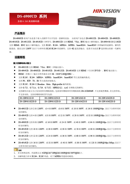
16 路 1080P@30fps 及以下分 32 路 1080P@30fps 及以下 或 64 路 1080P@30fps 及
辨率
分辨率
以下分辨率
画面分割数
1/4/6/8/9/12/16
1/4/6/8/9/12/16/25 1/4/6/8/9/12/16/25/36
外
网络接口
1 个 RJ45 10M/100M/
SXGA:1280*1024@60Hz,
720P:1280*720@60/50Hz,
XVGA:1280*960@60Hz, UXGA:1600*1200@60Hz,
1080p:1920*1080@60/50Hz,
WXGA:1280*800@60Hz/1366*768@60Hz,
输
WXGA+:1440*900@60Hz,
XVGA:1280*960@60Hz, UXGA:1600*1200@60Hz,1080p:1920*1080@60/50Hz,
输
WXGA:1280*800@60Hz/1366*768@60Hz,WXGA+:1440*900@60Hz,
入
WSXGA+:1680*1050@60Hz
参 DVI-I 输入分辨率 XGA:1024*768@60Hz/800*600@60Hz, SXGA:1280*1024@60Hz,720P:1280*720@60/50Hz,
DS-6912UD 支持 12 路 1200W,或 24 路 800W,或 36 路 500W,或 60 路 300W,或 96 路 1080P@30fps 及以下分辨率同 时实时解码;
DS-6916UD 支持 16 路 1200W,或 32 路 800W,或 48 路 500W,或 80 路 300W,或 128 路 1080P@30fps/3Mbps 及以下 分辨率同时实时解码;
推荐十款值得购买的HIFI解码器
推荐十款值得购买的HIFI解码器【HIFI说2015年11月报道】DAC解码器(芯片)又称数模转换器,DAC即Digital to Analog Converter,数字到模拟转换的芯片。
因为音乐是数字信号,而耳机、音箱等音响设备需要模拟信号,所以解码器需要将数字信号转换为模拟信号输出,从而驱动音箱、耳机等音响设备发出声音。
下面HIFI说就为您推荐最值得购买的解码器产品。
一、Monarchy Audio NM24 解码/前级(国外售价:1080美元)Monarchy Audio NM24 解码/前级“Monarchy Audio,是美国的富翁发烧友C.C.Poon于1979年在旧金山创立的Hi-End音响品牌……”二、Aurender Flow解码器(国外售价:1295 美元)Aurender Flow解码器“韩国 Aurender发布了它们首部有具有DAC功能的产品FLOW。
FLOW虽然自带储存装置,但由于本身没有播放器功能,所以播放时需要配合电脑、Android手机或平板等设备一起使用。
它内置mSATA 接口,可增配一个SSD作为储存媒体,最高容量支持1TB。
为了配合高速SSD传输数据,厂商使用USB 3.0的介面。
这款产品配备了ESS 的ES9018K2M芯片,支持最高384kHz/32bit的PCM音乐文件,而DSD档方面,则能够播放高达5.6MHz的DXD,而且还提供滤波器的切换……”三、Wyred 4 Sound DAC-2解码器(国外售价:1499 美元,增加DSD功能另加100美元,使用SE板卡另加1000美元)Wyred 4 Sound DAC-2解码器“老实说这是笔者第一次评测DAC,没想到就过上了很发烧的DAC-2DSD,经过一番研究后,笔者从中认识到许多设计DAC的要点,包含内部线路,以及各种输出入端子的规格,更在试听时实际验收成效。
W4S的设计功力是有目共睹的,他家掌握了电路设计的要点,几乎将成本(时间、金钱)都用在声音上,包括上述提到的全平衡放大电路、精密电阻、充沛电源、性能卓越的DAC芯片,这些对声音都有全面性改善,简直是数字流大补帖……”四、Mytek Stereo192-DSD解码器(国外售价:1595 美元)Mytek Stereo192-DSD解码器“MYTEK DIGITAL的Stereo 192 DSD DAC M与YAMAHA一样,是搭载了ESS制32bit DAC元件的袖珍D/A转换器。
Bryston BDA-2解码器
Bryston BDA-2解码器
无
【期刊名称】《中国电子商情:视听前线》
【年(卷),期】2013(000)001
【摘要】加拿大品牌Bryston(拜事通)继BDA-1后推出了全新的BDA-2解码器,该款解码器采用了双核32位AKMDAC芯片作数模转换,且该芯片是目前最高分辨率的芯片之一,配合Bryston高精度的精密振荡器采样,以减少任何可能的抖动。
输入部分采用最先进的异步USB传输,支持24bit/192kHz格式。
另外还配备有Bryston独特的阻抗配合转换器,以防止讯源流失。
【总页数】1页(P57-57)
【作者】无
【作者单位】不详
【正文语种】中文
【中图分类】TN764
【相关文献】
1.Bryston Model A3落地音箱 [J], 家祺;小路
2.拜事通Bryston Cubed系列4B3后级 [J],
3.Bryston拜事通BLP-1黑胶唱盘 [J],
4.声音精准性价比高 Bryston Mini A书架箱 [J], 司徒耀明;阿毕
5.Bryston家族越来越完整访Bryston总裁BrianW.Russell先生 [J], 本刊记者
因版权原因,仅展示原文概要,查看原文内容请购买。
中衡一款发烧DAC音频解码器的【设计明细】与制作
一款发烧音频解码器的设计与制作摘要:随着数字音频时代的来临,数字音源也不断丰富,然而这些数字音频设备内建的采用一体化设计,易受干扰,解码出来的声音并不尽人意。
一般的数字音源如、、网络机顶盒等都配备了光纤和同轴输出接口,把数字音频信号绕开机内的,直接送到专门的音频解码器,由专门的解码器完成转换,实现声音的高保真重放。
本文本着的设计原则,设计一款立体声音频解码器,由317、431组成多路甲类并联稳压供电,采用经典的高性能的8412负责数字信号的接收与解调、1700P 数字滤波、2R架构的1702做转换、挑选发烧运放担任和,完成数字信号的接收并转换成高保真的音频信号,再通过一级电子管校音线路,输出驱动信号可以直接推动后级的甲类晶体管功放。
实现效果的重放。
关键词:音频解码器 1702 电子管校音高保真甲类并联稳压1. 引言:一些低中档数字音源输出的音频声音生硬,数码声重,音质刺耳烦躁,不耐听,满足不了音响发烧友的听觉需求。
主要是因为这些机器内建的音频性能差,模拟滤波、放大器件普通,供电也过于简单造成。
好在这些机器一般都配有光纤或者同轴输出端口,提供数字音频信号输出,供高档的音频解码还原高保真的声音。
有动手能力的烧友都喜欢一台高性能的音频解码器以重放的音响效果,满足自己的听觉需求。
2. 音频解码器电路的设计2.1 音频解码器电路组成音频解码器由数字信号接收器、数字滤波器、转换器、转换器、滤波器将数字音频还原还原成模拟音频信号,再通过电子管组成的和田茂氏线路校音、开机延迟吸合电路控制输出模拟音频信号推动后级功放。
电路的组成及其信号流如图1:图1 音频解码器组成及信号流程2.2 数字信号接收与音频解码电路数字信号的接收与解码电路关系到音频信号还原的质量,想要得到高保真的声音,必需采用高性能的器件担当音频解码的重任,这是重点部分,电路原理图见图2,下面对其原理作进一步的分析:2.2.1 数字信号接收器数字信号接收采用美国公司的带有的解调芯片8412担任,能自动识别3248K采样率。
中移物联网有限公司CM32M4xxR芯片数据手册说明书
2 功能简介 ............................................................................................................................................................................. 16bit 基础定时计数器
― 1x 24bit SysTick
― 1x 7bit 窗口看门狗(WWDG)
― 1x 12bit 独立看门狗( IWDG)
编程方式
― 支持 2-wire/4-wire JTAG 在线调试接口
― 支持 UART Bootloader
安全特性
― 内置密码算法硬件加速引擎
CM32M4xxR芯片数据手册
中移物联网有限公司
CM32M4xxR系列芯片采用 32 bit RISC-V N308内核,最高工作主频144MHz,支持浮点运算和DSP指 令,集成多达512KB Flash、144KB SRAM、4x12bit 5Msps ADC、4xOPAMP、7xCOMP、2x1Msps 12bit DAC,支持多达24通道电容式触摸按键,集成多路U(S)ART、I2C、SPI、QSPI、CAN通信接口,内置密 码算法硬件加速引擎