Analog clock
Audio术语:Mixer,Mux,DAPM,Clock

Audio术语:Mixer,Mux,DAPM,ClockAudio DAPM widgets fall into a number of types:-o Mixer - Mixes several analog signals into a single analog signal.o Mux - An analog switch that outputs only one of many inputs.Mixer可以混合多个输⼊到输出Mux只能从多个输⼊⾥选择⼀个作为输出Mixer当然也可以只从多个输⼊⾥选择⼀个作为输出————————————————————————————————————Path domain widgets have a ability to control or affect the audio signal or audio paths within the audio subsystem. They have the following form:-SND_SOC_DAPM_PGA(name, reg, shift, invert, controls, num_controls)Any widget kcontrols can be set using the controls and num_controls members.e.g. Mixer widget (the kcontrols are declared first)static const snd_kcontrol_new_t wm8731_output_mixer_controls[] ={ SOC_DAPM_SINGLE("Line Bypass Switch", WM8731_APANA, 3, 1, 0),SOC_DAPM_SINGLE("Mic Sidetone Switch", WM8731_APANA, 5, 1, 0),SOC_DAPM_SINGLE("HiFi Playback Switch", WM8731_APANA, 4, 1, 0),};SND_SOC_DAPM_MIXER("Output Mixer", WM8731_PWR, 4, 1, wm8731_output_mixer_controls,ARRAY_SIZE(wm8731_output_mixer_controls)),Codec⾥有张audio path map,有很多interconnections:3. Codec Widget Interconnections ================================Widgets are connected to each other within the codec and machine by audio paths (called interconnections). Each interconnection must be defined in order to create a map of all audio paths between widgets.This is easiest with a diagram of the codec (and schematic of the machine audio system), as it requires joining widgets together via their audio signal paths.e.g., from the WM8731 output mixer (wm8731.c)The WM8731 output mixer has 3 inputs (sources)1. Line Bypass Input2. DAC (HiFi playback)3. Mic Sidetone InputEach input in this example has a kcontrol associated with it (defined in example above) and is connected to the output mixer via its kcontrol name. We can now connect the destination widget (wrt audio signal) with its source widgets.{"Output Mixer", "Line Bypass Switch", "Line Input"},{"Output Mixer", "HiFi Playback Switch", "DAC"},{"Output Mixer", "Mic Sidetone Switch", "Mic Bias"},So we have :-Destination Widget <=== Path Name <=== Source WidgetOr:-Sink, Path, SourceOr :-"Output Mixer" is connected to the "DAC" via the "HiFi Playback Switch".When there is no path name connecting widgets (e.g. a direct connection) we pass NULL for the path name. Interconnections are created with a call to:-snd_soc_dapm_connect_input(codec, sink, path, source);Finally, snd_soc_dapm_new_widgets(codec) must be called after all widgets and interconnections have been registered with the core. This causes the core to scan the codec and machine so that the internal DAPM state matches the physical state of the machine. ——————————————————————————————————————关于Clock,你只要知道MCLK和DAI的Clock,MCLK相当于整个CODEC的SYSCLK,给CODEC内部数字电路⽤的,⽐如产⽣ADC的采样率,或产⽣DAC的采样率转换⽽DAI的Clock:document⾥说BCLK最好尽可能⼩,以节省功耗,且最好由codec来作为主,这样codec的采样率更准,但不知道为什么In general it is best to configure BCLK to the lowest possible speed (depending on your rate, number of channels and word size) to save on power.It is also desirable to use the codec (if possible) to drive (or master) the audio clocks as it usually gives more accurate samplerates than the CPU.。
Analog Devices ADXL193单轴高g iMEMS加速度计数据手册说明书

Single-Axis, High-g , i MEMS ® AccelerometersADXL193Rev. AInformation furnished by Analog Devices is believed to be accurate and reliable. However, no responsibility is assumed by Analog Devices for its use, nor for any infringements of patents or other rights of third parties that may result from its use. Specifications subject to change without notice. No license is granted by implication or otherwise under any patent or patent rights of Analog Devices. Trademarks and registered trademarks are the property of their respective owners.One Technology Way, P.O. Box 9106, Norwood, MA 02062-9106, U.S.A. Tel: 781.329.4700 Fax: 781.461.3113 ©2005 Analog Devices, Inc. All rights reserved.FEATURESComplete acceleration measurement system on a single monolithic ICAvailable in ±120 g or ±250 g output full-scale ranges Full differential sensor and circuitry for high resistance to EMI/RFIEnvironmentally robust packagingComplete mechanical and electrical self-test on digital commandOutput ratiometric to supplySensitive axes in the plane of the chip High linearity (0.2% of full scale) Frequency response down to dc Low noiseLow power consumption (1.5 mA)Tight sensitivity tolerance and 0 g offset capability Largest available prefilter clipping headroom 400 Hz, 2-pole Bessel filter Single-supply operationCompatible with Sn/Pb and Pb-free solder processesAPPLICATIONSVibration monitoring and control Vehicle collision sensing Shock detectionGENERAL DESCRIPTIONThe ADXL193 is a low power, complete single-axisaccelerometer with signal conditioned voltage outputs that are all on a single monolithic IC. This product measures acceleration with a full-scale range of ±120 g or ±250 g (minimum). It can also measure both dynamic acceleration (vibration) and static acceleration (gravity).The ADXL193 is a fourth-generation surface micromachined i MEMS® accelerometer from ADI with enhanced performance and lower cost. Designed for use in front and side impact airbag applications, this product also provides a complete cost-effective solution useful for a wide variety of other applications. The ADXL193 is temperature stable and accurate over theautomotive temperature range, with a self-test feature that fully exercises all the mechanical and electrical elements of the sensor with a digital signal applied to a single pin. The ADXL193 is available in a 5 mm × 5 mm × 2 mm, 8-terminal ceramic LCC package.FUNCTIONAL BLOCK DIAGRAM05366-001X OUTFigure 1.ADXL193Rev. A | Page 2 of 12TABLE OF CONTENTSSpecifications.....................................................................................3 Absolute Maximum Ratings............................................................4 ESD Caution..................................................................................4 Pin Configuration and Function Descriptions.............................5 Theory of Operation........................................................................7 Applications.......................................................................................8 Power Supply Decoupling............................................................8 Self-Test..........................................................................................8 Clock Frequency Supply Response.............................................8 Signal Distortion...........................................................................8 Outline Dimensions..........................................................................9 Ordering Guide.. (9)REVISION HISTORY5/05—Rev. 0 to Rev. AADXL193Rev. A | Page 3 of 12SPECIFICATIONS 1At T A = −40°C to +105°C, 5.0 V dc ± 5%, acceleration = 0 g ; unless otherwise noted. Table 1.Model No. AD22282Model No. AD22283Parameter Conditions Min Typ Max Min Typ Max Unit SENSOR Output Full-Scale Range I OUT ≤ ±100 μA 120 250 gNonlinearity 0.2 2 0.2 2 %Package Alignment Error 1 1 Degree Cross-Axis Sensitivity −5 +5 −5 +5 % Resonant Frequency24 24 kHz Sensitivity, Ratiometric(Over Temperature) V DD = 5 V, 100 Hz 17.1 18 18.9 7.6 8 8.4 mV/g OFFSETZero-g Output Voltage(Over Temperature)2V OUT − V DD /2, V DD = 5 V −125 +125 −100 +100 mVNOISE Noise Density 10 Hz − 400 Hz, 5 V 3 10 5 15 m g /√Hz Clock Noise 5 5 mV p-p FREQUENCY RESPONSE Two-pole Bessel −3 dB Frequency 360 400 440 360 400 440 Hz−3 dB Frequency Drift 25°C to T MIN or T MAX2 2 Hz SE L F-TESTOutput Change(Cube vs. V DD )3V DD = 5 V 400 500 600 200 250 300 mV Logic Input High V DD = 5 V 3.5 3.5 V Logic Input Low V DD = 5 V 1 1 V Input Resistance Pull-down resistor to GND 30 50 30 50kΩOUTPUT AMP L IFIER Output Voltage Swing I OUT = ±400 μA 0.25 V DD − 0.25 0.25 V DD − 0.25 V Capacitive Load Drive 1000 1000 pF PREFI L TER HEADROOM 800 1400 g CFSR @ 400 kHz 21.5 V/V POWER SUPPLY (V DD ) 4.75 5.25 4.75 5.25 V Functional Range 3.5 6 3.5 6 V Quiescent Supply Current V DD = 5 V 1.5 21.5 2 mA TEMPERATURE RANGE−40 +125−40 +125°C1 All minimum and maximum specifications are guaranteed. Typical specifications are not guaranteed. 2Zero g output is ratiometric. 3Self-test output at V DD = (Self-Test Output at 5 V) × (V DD /5 V)3.ADXL193Rev. A | Page 4 of 12ABSOLUTE MAXIMUM RATINGSTable 2.Parameter RatingAcceleration (Any Axis, Unpowered) 4,000 gAcceleration (Any Axis, Powered) 4,000 gV S −0.3 V to +7.0 VAll Other Pins (COM − 0.3 V) to(V S + 0.3 V) Output Short-Circuit Duration (Any Pin to Common)Indefinite Operating Temperature Range −65°C to +150°CStorage Temperature −65°C to +150°CStresses above those listed under Absolute Maximum Ratings may cause permanent damage to the device. This is a stress rating only; functional operation of the device at these or any other conditions above those indicated in the operational section of this specification is not implied. Exposure to absolute maximum rating conditions for extended periods may affect device reliability.ESD CAUTIONESD (electrostatic discharge) sensitive device. Electrostatic charges as high as 4000 V readily accumulate on the human body and test equipment and can discharge without detection. Although this product features proprietary ESD protection circuitry, permanent damage may occur on devices subjected to high energy electrostatic discharges. Therefore, proper ESD precautions are recommended to avoid performancedegradation or loss of functionality.ADXL193Rev. A | Page 5 of 12PIN CONFIGURATION AND FUNCTION DESCRIPTIONS05366-002NC = NO CONNECTNCNC COM V DD X OUT NCSTVFigure 2. Pin ConfigurationTable 3. Pin Function DescriptionsPin No. Mnemonic Description 1 NC Do Not Connect 2 NCDo Not Connect3 COM Common4 ST Self-Test5 NC Do Not Connect6 X OUT X Channel Output7 V DD 3.5 V to 6 V8 V DD23.5 V to 6 VADXL193Rev. A | Page 6 of 12T E M P E R A T U R ETIMET TFigure 3. Recommended Soldering ProfileTable 4. Recommended Soldering ProfileProfile Feature Sn63/Pb37 Pb-Free AVERAGE RAMP RATE (T L TO T P ) 3°C/s max3°C/s maxPREHEATMinimum Temperature (T SMIN ) 100°C 150°C Maximum Temperature (T SMAX ) 150°C 200°C TIME (T SMIN TO T SMAX ), t S 60 s − 120 s 60 s − 150 s T SMAX TO T L Ramp-Up Rate 3°C/s 3°C/s TIME MAINTAINED ABOVE LIQUIDOUS (T L ) Liquidous Temperature (T L ) 183°C 217°C Time (t L ) 60 s − 150 s60 s − 150 s PEAK TEMPERATURE (T P ) 240°C + 0°C/−5°C 260°C + 0°C/−5°C TIME WITHIN 5°C OF ACTUAL PEAK TEMPERATURE (t P ) 10 s − 30 s 20 s − 40 s RAMP-DOWN RATE 6°C/s max 6°C/s max TIME 25°C TO PEAK TEMPERATURE 6 min max 8 min max05366-004EARTH'S SURFACE= 2.482VXXXXX XXXX22282X OUT = 2.500VX X X X X X X X X22282X X X X X X X X X22282X OUT = 2.500V X OUT = 2.518VX OUT = 2.500VFigure 4. Output Response vs. OrientationADXL193Rev. A | Page 7 of 12THEORY OF OPERATIONThe ADXL193 provides a fully differential sensor structure and circuit path, resulting in the industry’s highest resistance to EMI/RFI effects. This latest generation uses electrical feedback with zero-force feedback for improved accuracy and stability. The sensor resonant frequency is significantly higher than the signal bandwidth set by the on-chip filter, avoiding the signal analysis problems caused by resonant peaks near the signal bandwidth.Figure 5 is a simplified view of one of the differential sensor elements. Each sensor includes several differential capacitor unit cells. Each cell is composed of fixed plates attached to the substrate and movable plates attached to the frame.Displacement of the frame changes the differential capacitance, which is measured by the on-chip circuitry.Complementary 400 kHz square waves drive the fixed plates. Electrical feedback adjusts the amplitudes of the square waves such that the ac signal on the moving plates is 0. The feedback signal is linearly proportional to the applied acceleration. This unique feedback technique ensures that there is no net electrostatic force applied to the sensor. The differentialfeedback control signal is also applied to the input of the filter, where it is filtered and converted to a single-ended signal. 05366-005UNIT SENSINGCELLUNITFORCING CELLFigure 5. Simplified View of Sensor Under AccelerationADXL193Rev. A | Page 8 of 12APPLICATIONSPOWER SUPPLY DECOUPLINGFor most applications, a single 0.1 μF capacitor, C DC , adequately decouples the accelerometer from noise on the power supply. However, in some cases, particularly where noise is present at the 400 kHz internal clock frequency (or any harmonic thereof), noise on the supply can cause interference on the ADXL193’s output. If additional decoupling is needed, a 50 Ω (or smaller) resistor or ferrite bead can be inserted in the supply line. Additionally, a larger bulk bypass capacitor (in the 1 μF to 4.7 μF range) can be added in parallel to C DC .SELF-TESTThe fixed fingers in the forcing cells are normally kept at the same potential as that of the movable frame. When the self-test digital input is activated, the voltage on the fixed fingers on one side of the moving plate in the forcing cells is changed. This creates an attractive electrostatic force, which causes the frame to move toward those fixed fingers. The entire signal channel is active; therefore, the sensor displacement causes a change in V OUT . The ADXL193’s self-test function is a comprehensive method of verifying the operation of the accelerometer. Because electrostatic force is independent of the polarity of the voltage across capacitor plates, a positive voltage is applied in half of the forcing cells, and its complement in the other half of the forcing cells. Activating self-test causes a step function force to be applied to the sensor, while the capacitive coupling term is canceled. The ADXL193 has improved self-test functionality, including excellent transient response and high speed switching capability. Arbitrary force waveforms can be applied to the sensor by modulating the self-test input, such as test signals to measure the system frequency response, or even crash signals to verify algorithms within the limits of the self-test swing. The ST pin should never be exposed to voltages greater than V S + 0.3 V . If this cannot be guaranteed due to the systemdesign (for instance, if there are multiple supply voltages), then a low V F clamping diode between ST and V S is recommended.CLOCK FREQUENCY SUPPLY RESPONSEIn any clocked system, power supply noise near the clock frequency may have consequences at other frequencies. An internal clock typically controls the sensor excitation and the signal demodulator for micromachined accelerometers. If the power supply contains high frequency spikes, they may be demodulated and interpreted as an acceleration signal. A signal appears as the difference between the noise frequency and the demodulator frequency. If the power supply spikes are 100 Hz away from the demodulator clock, there is an output term at 100 Hz. If the power supply clock is at exactly the same frequency as the accelerometer clock, the term appears as an offset.If the difference frequency is outside of the signal bandwidth, the filter attenuates it. However, both the power supply clock and the accelerometer clock may vary with time or temperature, which can cause the interference signal to appear in the output filter bandwidth.The ADXL193 addresses this issue in two ways. First, the high clock frequency eases the task of choosing a power supply clock frequency such that the difference between it and the accelero-meter clock remains well outside of the filter bandwidth.Second, the ADXL193 is the only micromachined accelerometer to have a fully differential signal path, including differential sensors. The differential sensors eliminate most of the power supply noise before it reaches the demodulator. Good highfrequency supply bypassing, such as a ceramic capacitor close to the supply pins, also minimizes the amount of interference. The clock frequency supply response (CFSR) is the ratio of the response at V OUT to the noise on the power supply near the accelerometer clock frequency. A CFSR of 3 means that the signal at V OUT is 3× the amplitude of an excitation signal at V DD near the accelerometer internal clock frequency. This is analogous to the power supply response, except that the stimulus and the response are at different frequencies. The ADXL193’s CFSR is 10× better than a typical single-ended accelerometer system.SIGNAL DISTORTIONSignals from crashes and other events may contain high amplitude, high frequency components. These components contain very little useful information and are reduced by the 2-pole Bessel filter at the output of the accelerometer. However, if the signal saturates at any point, the accelerometer output does not look like a filtered version of the acceleration signal. The signal may saturate anywhere before the filter. For example, if the resonant frequency of the sensor is low, the displacement per unit acceleration is high. The sensor may reach the mechanical limit of travel if the applied acceleration is high enough. This can be remedied by locating the accelerometer where it does not see high values of acceleration and by using a higher resonant frequency sensor, such as the ADXL193.Also, the electronics may saturate in an overload condition between the sensor output and the filter input. Ensuring that internal circuit nodes operate linearly to at least several times the full-scale acceleration value can minimize electricalsaturation. The ADXL193 circuit is linear to approximately 8× full scale.ADXL193Rev. A | Page 9 of 12OUTLINE DIMENSIONSBOTTOM VIEWFigure 6. 8-Terminal Ceramic Leadless Chip Carrier [LCC](E-8)Dimensions shown in millimetersADXL193 ORDERING GUIDEModel 1Parts per Reel MeasurementRange SpecifiedVoltage (V) TemperatureRange PackageDescription Package Option AD22282-A-R2 250 ±120 g 5 −40°C to +125°C 8-Terminal Ceramic Leadless Chip Carrier E-8 AD22282-A 3000 ±120 g 5 −40°C to +125°C 8-Terminal Ceramic Leadless Chip Carrier E-8 AD22283-B-R2 250 ±250 g 5 −40°C to +125°C 8-Terminal Ceramic Leadless Chip Carrier E-8 AD22283-B 3000 ±250 g5 −40°C to +125°C 8-Terminal Ceramic Leadless Chip Carrier E-81All models are on tape and reel and are Pb-free parts.ADXL193NOTESRev. A | Page 10 of 12ADXL193 NOTESRev. A | Page 11 of 12ADXL193NOTES©2005 Analog Devices, Inc. All rights reserved. Trademarks andregistered trademarks are the property of their respective owners.D05366–0–5/05(A)Rev. A | Page 12 of 12。
Analog and Digital(模拟电子和数字电子)电子信息专业英语文章

Analog and Digital(模拟电子和数字电子)英文原稿:Analog and DigitalIdeal Operational Amplifiers and Practical Limitations In order to discuss the ideal parameters of operational amplifiers, we must firstdefine the terms, and then go on to describe what we regard as the ideal values forthose terms. At first sight, the specification sheet for an operational amplifier seems to list a large number of values, some in strange units, some interrelated, and often confusing to those unfamiliar with the subject. The approach to such a situation is to be methodical, and take the necessary time to read and understand each definition in the order that it is listed. Without a real appreciation of what each means, the designer is doomed to failure. The objective is to be able to design a circuit from the basis of the published data, and know that it will function as predicted when the prototype is constructed.1It is all too easy with linear circuits, which appear relatively simple when compared with today’s complex logic arrangements, to ignore detailed performance parameters which can drastically reduce the expected performance.Let us take a very simple but striking example. Consider a requirement for anamplifier having a voltage gain of 10 at 50 kHz driving into a 10 k load. A commonlow-cost, internally frequency-compensated op amp is chosen; it has the requiredbandwidth at a closed-loop gain of 10, and it would seem to meet the bill. The deviceis connected, and it is found to have the correct gain. But it will only produce a fewvolts output swing when the data clearly shows that the output should be capable ofdriving to within two or three volts of the supply rails. The designer has forgotten thatthe maximum output voltage swing is severely limited by frequency, and that themaximum low-frequency output swing becomes limited at about 10 kHz. Of course,the information is in fact on the data sheet, but its relevance has not been appreciated.This sort of problem occurs regularly for the inexperienced designer. So the moral isclear: always take the necessary time to write down the full operating requirementsbefore attempting a design. Attention to the detail of the performance specificationwill always be beneficial. It is suggested the following list of performance details beconsidered:1. Closed loop gain accuracy, stability with temperature, time and supply voltage2. Power supply requirements, source and load impedances, power dissipation3. Input error voltages and bias currents. Input and output resistance, drift withtime and temperature4. Frequency response, phase shift, output swing, transient response, slew rate,frequency stability, capacitive load driving, overload recovery5. Linearity, distortion and noise6. Input, output or supply protection required. Input voltage range,common-mode rejection7. External offset trimming requirementNot all of these terms will be relevant, but it is useful to remember that it is better to consider them initially rather than to be forced into retrospective modifications.All parameters are subject to wide variationsNever forget this fact. How many times has a circuit been designed using typical values, only to find that the circuit does not work because the device used is not typical? The above statement thus poses a tricky question: when should typical values and when should worst-case values be used in the design? This is where the judgment of the experienced designer must be brought to bear. Clearly, if certain performance requirements are mandatory, then worst-case values must be used. In many cases, however, the desirability of a certain defined performance will be a compromise between ease of implementation, degree of importance, and economic considerations. Do not over-specify or over-designIn the end, we are all controlled by cost, and it is really pointless taking a sledgehammer to crack a nut, Simplicity is of the essence since the low parts count implementation is invariably cheaper and more reliable.As an example of this judgment about worst-case design, consider a low-gain DC transducer amplifier required to amplify 10 mV from a voltage source to produce an output of .l V with an accuracy of ±1% over a temperature range of 0~70︒C. Notice that the specification calls for an accuracy of ±1%. This implies that the output should be 1 V ±10 mV from 0 ~ 70︒C. The first step is, of course, to consider our list above, and decide which of the many parameters are relevant. Two of the most important to this (very limited) specification are offset voltage drift and gain stability with temperature. We will assume that all initial errors are negligible (rarely the case in practice). The experienced designer would know that most op amps have a very large open-loop gain, usually very much greater than 10000. A closed-loop gain change of ±1% implies that the loop gain (as explained later) should change by less than ±100% for a closed-loop gain of 100. This is clearly so easily fulfilled that the designer knows immediately that he can use typical open-loop gain values in his calculations. However, offset voltage drift is another matter. Many op amp specifications include only typical values for offset voltage drift; this may well be in the order of 5 μV/︒C, with an unquoted maximum for any device of 30 μV/︒C. If by chance we use a device which has this worst-case drift, then the amplifier error could be 30×70=2100 μV=2.1 mV over temperature, which is a significant proportion of our total allowable error from all sources.Here is a case, then, where one can be confident that the typical value of open-loop gain can be used, but where the maximum value of drift may well cause significant errors. This sort of judgment is essential in careful design, and great care is required in interpreting manufacturers’ data. This consideration must be extended toall the details listed above apart from the fact that worst-case values are often not quoted. It is often found that values given are not 100% tested. Statistical testing is employed which, for example, guarantees that 90% of all devices fall within the range specified. It could be very inconvenient for the user who relies on the specified performance and then finds that he has several of the ‘other’ 10% actually plugged into his circuit.Data Registers and CountersData registerThe simplest type of register is a data register, which is used for the temporary storage of a “word” of data. In its simplest form, it consists of a set of N D flip-flops, all sharing a common clock. All of the digits in the N bit data word are connected to the data register by an N-line “data bus”. Figure 1.1 shows a 4 bit data register, implemented with four D flip-flops. The data register is said to be a synchronous device, because all the flip-flops change state at the same time.Shift registersAnother common form of register used in computers and in many other types of logic circuits is a shift register. It is simply a set of flip-flops (usually D latches or RS flip-flops) connected together so that the output of one becomes the input of the next, and so on in series. It is called a shift register because the data is shifted through the register by one bit position on each clock pulse. Figure 1.2 shows a 4 bit shift register, implemented with D flip-flops.On the leading edge of the first clock pulse, the signal on the DATA input is latched in the first flip-flop. On the leading edge of the next clock pulse, the contents of the first flip-flop is stored in the second flip-flop, and the signal which is present at the DATA input is stored in the first flip-flop, etc. Because the data is entered one bit at a time, this called a serial-in shift register. Since there is only one output, and data leaves the shift register one bit at a time, then it is also a serial out shift register. (Shift registers are named by their method of input and output; either serial or parallel.) Parallel input can be provided through the use of the preset and clear inputs to the flip-flop. The parallel loading of the flip-flop can be synchronous (i.e., occurs with the clock pulse) or asynchronous (independent of the clock pulse) depending on the design of the shift register. Parallel output can be obtained from the outputs of each flip-flop as shown in Figure 1.3.Communication between a computer and a peripheral device is usually done serially, while computation in the computer itself is usually performed with parallel logic circuitry. A shift register can be used to convert information from serial form to parallel form, and vice versa. Many different kinds of shift registers are available, depending upon the degree of sophistication required.Counters — weighted coding of binary numbersIn a sense, a shift register can be considered a counter based on the unary numbersystem. Unfortunately, a unary counter would require a flip-flop for each number in the counting range. A binary weighted counter, however, requires only flip-flops to count to N. A simple binary weighted counter can be made using T flip-flops. The flip-flops are attached to each other in a way so that the output of one acts as the clock for the next, and so on. In this case, the position of the flip-flop in the chain determines its weight; i.e., for a binary counter, the “power of two” it corresponds to.A 3-bit (modulo 8) binary counter could be configured with T flip-flops as shown in Figure 1.4. A timing diagram corresponding to this circuit is shown in Figure 1.5.Note that a set of lights attached to O0, O1, O2 would display the numbers of full clock pulses which had been completed, in binary (modulo 8), from the first pulse. As many T flip-flops as required could be combined to make a counter with a large number of digits.Note that in this counter, each flip-flops changes state on the falling edge of the pulse from the previous flip-flop. Therefore there will be a slight time delay, due to the propagation delay of the flip-flops between the time one flip-flop changes state and the time the next one changes state, i.e., the change of state ripples through the counter, and these counters are therefore called ripple counters. As in the case of a ripple carry adder, the propagation delay can become significant for large counters.It is possible to make, or buy in a single chip, counters which will count up, count down, and which can be preset to any desired number. Counters can also be constructed which count in BCD and base 12 or any other number base.A count down counter can be made by connecting the Q output to the clock input in the previous counter. By the use of preset and clear inputs, and by gating the output of each T flip- flop with another logic level using AND gates (say logic 0 for counting down, logic 1 for counting up), then a presetable up-down binary counter can be constructed. Figure 1.6 shows an up-down counter, without preset or clear.Synchronous countersThe counters shown previously have been “asynchronous counters”; so called because the flip-flops do not all change state at the same time, but change as a result of a previous output. The output of one flip-flop is the input to the next; the state changes consequently “ripple through” the flip-flops, requiring a time proportional to the length of the counter. It is possible to design synchronous counters, using JK flip-flops, where all flip-flops change state at the same time; i.e., the clock pulse is presented to each JK flip-flop at the same time. This can be easily done by nothing that, for a binary counter, any given digit changes its value (from 1 to 0 or from 0 to 1) whenever all the previous digits have a value of 1. A count down timer can be made by connecting the Q output to the J and K, through the AND gates. Preset and clear could also be provided, and the counter could be made “programmable” as in the previous case.The timing diagram is similar to that shown for the asynchronous (ripple) counters, except that the ripple time is now zero; all counters clock at the same time. It is common for synchronous counters to trigger on the positive edge of the clock,rather than the trailing edge.Nature of Phase LockThe phase detector compares the phase of a periodic input signal against the phase of the VCO. Output of PD is a measure of the phase difference between its two inputs. The difference voltage is then filtered by the loop filter and applied to the VCO. Control voltage on the VCO changes the frequency in a direction that reduces the phase difference between the input signal and the local oscillator.When the loop is locked, the control voltage is such that the frequency of the VCO is exactly equal to the average frequency of the input signal. For each cycle of input there is one, and only one, cycle of oscillator output. One obvious application of phase lock is in automatic frequency control (AFC). Perfect frequency control can be achieved by this method, whereas conventional AFC techniques necessarily entail some frequency error.To maintain the control voltage needed for lock it is generally necessary to have a nonzero output from the phase detector. Consequently, the loop operates with some phase error present. As a practical matter, however, this error tends to be small in a well-designed loop.A slightly different explanation may provide a better understanding of loop operation. Let us suppose that the incoming signal carries information in its phase or frequency; this signal is inevitably corrupted by additive noise. The task of a phase lock receiver is to reproduce the original signal while removing as much of the noise as possible.To reproduce the signal the receiver makes use of a local oscillator whose frequency is very close to that expected in the signal. Local oscillator and incoming signal waveforms are compared with one another by a phase detector whose error output indicates instantaneous phase difference. To suppress noise the error is averaged over some length of time, and the average is used to establish frequency of the oscillator.If the original signal is well behaved (stable in frequency), the local oscillator will need very little information to be able to track, and that information can be obtained by averaging for a long period of time, thereby eliminating noise that could be very large. The input to the loop is a noisy signal, whereas the output of the VCO is a cleaned-up version of the input. It is reasonable, therefore, to consider the loop as a kind of filter that passes signals and rejects noise.Two important characteristics of the filter are that the bandwidth can be very small and that the filter automatically tracks the signal frequency. These features, automatic tracking and narrow bandwidth, account for the major uses of phase lock receivers. Narrow bandwidth is capable of rejecting large amounts of noise; it is not at all unusual for a PLL to recover a signal deeply embedded in noise.History and applicationAn early description of phase lock was published by de Bellescize in 1932 and treated the synchronous reception of radio signals. Superheterodyne receivers hadcome into use during the 1920s, but there was a continual search for a simpler technique; one approach investigated was the synchronous, or homodyne, receiver. In essence, this receiver consists of nothing but a local oscillator, a mixer, and an audio amplifier. To operate, the oscillator must be adjusted to exactly the same frequency as the carrier of the incoming signal, which is then converted to an intermediate frequency of exactly 0 Hz. Output of the mixer contains demodulated information that is carried as sidebands by the signal. Interference will not be synchronous with the local oscillator, and therefore mixer output caused by an interfering signal is a beat-note that can be suppressed by audio filtering.Correct tuning of the local oscillator is essential to synchronous reception; any frequency error whatsoever will hopelessly garble the information. Furthermore, phase of the local oscillator must agree, within a fairly small fraction of a cycle, with the received carrier phase. In other words, the local oscillator must be phase locked to the incoming signal.For various reasons the simple synchronous receiver has never been used extensively. Present-day phase lock receivers almost invariably use the superheterodyne principle and tend to be highly complex. One of their most important applications is in the reception of the very weak signals from distant spacecraft. The first widespread use of phase lock was in the synchronization of horizontal and vertical scan in television receivers. The start of each line and the start of each interlaced half-frame of a television picture are signaled by a pulse transmitted with the video information. As a very crude approach to reconstructing a scan raster on the TV tube, these pulses can be stripped off and individually utilized to trigger a pair of single sweep generators.A slightly more sophisticated approach uses a pair of free-running relaxation oscillators to drive the sweep generators. In this way sweep is present even if synchronization is absent.Free-running frequencies of the oscillators are set slightly below the horizontal and vertical pulse rates, and the stripped pulses are used to trigger the oscillators prematurely and thus to synchronize them to the line and half-frame rates (half-frame because United States television interlaces the lines on alternate vertical scans).In the absence of noise this scheme can provide good synchronization and is entirely adequate. Unfortunately, noise is rarely absent, and any triggering circuit is particularly susceptible to it. As an extreme, triggered scan will completely fail at a signal-to-noise ratio that still provides a recognizable, though inferior, picture.Under less extreme conditions noise causes starting-time jitter and occasional misfiring far out of phase. Horizontal jitter reduces horizontal resolution and causes vertical lines to have a ragged appearance. Severe horizontal misfiring usually causes a narrow horizontal black streak to appear.Vertical jitter causes an apparent vertical movement of the picture. Also, the interlaced lines of successive half-frames would so move with respect to one another that further picture degradation would result.Noise fluctuation can be vastly reduced by phase locking the two oscillators to the stripped sync pulses. Instead of triggering on each pulse a phase-lock techniqueexamines the relative phase between each oscillator and many of its sync pulses and adjusts oscillator frequency so that the average phase discrepancy is small.Because it looks at many pulses, a phase lock synchronizer is not confused by occasional large noise pulses that disrupt a triggered synchronizer. The flywheel synchronizers in present day TV receivers are really phase-locked loops. The name “flywheel” is used because the circuit is able to coast through periods of increased noise or weak signal. Substantial improvement in synchronizing performance is obtained by phase-lock.In a color television receiver, the color burst is synchronized by a phase-lock loop.Space flight requirements inspired intensive application of phase lock methods. Space use of phase lock began with the launching of the first American artificial satellites. These vehicles carried low-power (10 mW) CW transmitters; received signals were correspondingly weak. Because of Doppler shift and drift of the transmitting oscillator, there was considerable uncertainty about the exact frequency of the received signal. At the 108 MHz frequency originally used, the Doppler shift could range over a ±3 kHz interval.With an ordinary, fixed-tuned receiver, bandwidth would therefore have to be at least 6 kHz, if not more. However, the signal itself occupies a very narrow spectrum and can be contained in something like a 6 Hz bandwidth.Noise power in the receiver is directly proportional to bandwidth. Therefore, if conventional techniques were used, a noise penalty of 1000 times (30 dB) would have to be accepted. The numbers have become even more spectacular as technology has progressed; transmission frequencies have moved up to S-band, making the Doppler range some ±75 kHz, whereas receiver bandwidths as small as 3 Hz have been achieved. The penalty for conventional techniques would thus be about 47 dB. Such penalties are intolerable and that is why narrowband, phase-locked, tracking receivers are used.Noise can be rejected by a narrowband filter, but if the filter is fixed the signal almost never will be within the pass-band. For a narrow filter to be usable it must be capable of tracking the signal. A phase-locked loop is capable of providing both the narrow bandwidth and the tracking that are needed. Moreover, extremely narrow bandwidths can be conveniently obtained (3 to 1000 Hz are typical for space applications); if necessary, bandwidth is easily changed.For a Doppler signal the information needed to determine vehicle velocity is the Doppler shift. A phase-lock receiver is well adapted to Doppler recovery, for it has no frequency error when locked.Other applicationsThe following applications, further discussed elsewhere in the book, represent some of the current uses of phase-lock.1. One method of tracking moving vehicles involves transmitting a coherentsignal to the vehicle, offsetting the signal frequency, and re-transmitting back to the ground. The coherent transponder in the vehicle must operate so that the input and output frequencies are exactly related in the ratio m/n, where m and nare integers. Phase-lock techniques are often used to establish coherence.2. A phase-locked loop can be used as a frequency demodulator, in which it hassuperior performance to a conventional discriminator.3. Noisy oscillators can be enclosed in a loop and locked to a clean signal. If theloop has a wide bandwidth, the oscillator tracks out its own noise and its output is greatly cleaned up.4. Frequency multipliers and dividers can be built by using PLLs.5. Synchronization of digital transmission is typically obtained by phase-lockmethods.6. Frequency synthesizers are conveniently built by phase-lock loops.中文翻译:模拟电子和数字电子理想运算放大器和实际限制为了讨论运算放大器的理想参数,我们必须首先定义一些指标项,然后对这些指标项讲述我们所认为的理想值。
ICL7139数字万用表电路
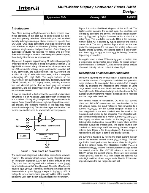
It may be beneficial to first review the concept of dual-slope conversion. It is an Analog to Digital conversion technique that is a subclass of integrating/charge-balancing conversion techniques. Some typical features are: high input impedance, excellent linearity, and excellent rejection to line-frequency noise (normal mode rejection). Two disadvantages are the slow conversion rate and the need for several external components.
最全Proteus元件库元件名称及中英对照

最全Proteus元件库元件名称及中英对照Proteus元件库元件名称及中英对照AND 与门ANTENNA 天线BA TTERY 直流电源BELL 铃,钟BVC 同轴电缆接插件BRIDEG 1 整流桥(二极管) BRIDEG 2 整流桥(集成块) BUFFER 缓冲器BUZZER 蜂鸣器CAP 电容CAPACITOR 电容CAPACITOR POL 有极性电容CAPV AR 可调电容CIRCUIT BREAKER 熔断丝COAX 同轴电缆CON 插口CRYSTAL 晶体整荡器DB 并行插口DIODE 二极管DIODE SCHOTTKY 稳压二极管DIODE VARACTOR 变容二极管DPY_3-SEG 3段LEDDPY_7-SEG 7段LEDDPY_7-SEG_DP 7段LED(带小数点) ELECTRO 电解电容FUSE 熔断器INDUCTOR 电感INDUCTOR IRON 带铁芯电感INDUCTOR3 可调电感JFET N N沟道场效应管JFET P P沟道场效应管LAMP 灯泡LAMP NEDN 起辉器LED 发光二极管METER 仪表MICROPHONE 麦克风MOSFET MOS管MOTOR AC 交流电机MOTOR SERVO 伺服电机NAND 与非门NOR 或非门NOT 非门NPN NPN三极管NPN-PHOTO 感光三极管OPAMP 运放OR 或门PHOTO 感光二极管PNP 三极管NPN DAR NPN三极管PNP DAR PNP三极管POT 滑线变阻器PELAY-DPDT 双刀双掷继电器RES1.2 电阻RES3.4 可变电阻RESISTOR BRIDGE ? 桥式电阻RESPACK ? 电阻SCR 晶闸管PLUG ? 插头PLUG AC FEMALE 三相交流插头SOCKET ? 插座SOURCE CURRENT 电流源SOURCE VOLTAGE 电压源SPEAKER 扬声器SW ? 开关SW-DPDY ? 双刀双掷开关SW-SPST ? 单刀单掷开关SW-PB 按钮THERMISTOR 电热调节器TRANS1 变压器TRANS2 可调变压器TRIAC ? 三端双向可控硅TRIODE ? 三极真空管V ARISTOR 变阻器ZENER ? 齐纳二极管DPY_7-SEG_DP 数码管SW-PB 开关元件名称中文名说明7407 驱动门1N914 二极管74Ls00 与非门74LS04 非门74LS08 与门74LS390 TTL 双十进制计数器7SEG 4针BCD-LED 输出从0-9 对应于4 根线的BCD码7SEG 3-8译码器电路BCD-7SEG转换电路AlterNATOR 交流发电机AMMETER-MILLI mA安培计AND 与门BA TTERY 电池/电池组BUS 总线CAP 电容CAPACITOR 电容器CLOCK 时钟信号源CRYSTAL 晶振Compim 串口D-FLIPFLOP D触发器FUSE 保险丝GROUND 地LAMP 灯LED-RED 红色发光二极管LM016L 2行16列液晶可显示2行16列英文字符,有8位数据总线D0-D7,RS,R/W,EN三个控制端口(共14线),工作电压为5V。
ANALOG DEVICES EE-248 数据手册

Engineer-to-Engineer NoteEE-248aTechnical notes on using Analog Devices DSPs, processors and development tools**********************************************************************************Or visit our on-line resources /ee-notes and /processorsInterfacing AD7676 ADCs to ADSP-21365 SHARC® ProcessorsContributed by Aseem Vasudev Prabhugaonkar and Jagadeesh RayalaRev 1 – October 7, 2004Copyright 2004, Analog Devices, Inc. All rights reserved. Analog Devices assumes no responsibility for customer product design or the use or application of customers’ products or for any infringements of patents or rights of others which may result from Analog Devices assistance. All trademarks and logos are property IntroductionThis application note explains how to interface AD7676 ADCs in master serial mode (internal discontinuous clock) to ADSP-21365 SHARC® processors. This application note also provides example code to demonstrate how the ADSP-21365 processor’s Serial Port (SPORT) can be programmed to receive data from the AD7676 converter when the AD7676 is configured in master serial mode, supplying a discontinuous serial data clock to the processor’s SPORT interface.About AD7676 ADCsAD7676 ADCs are 16-bit, 500 kSPS, charge-redistribution SAR, fully differential analog-to-digital converters (ADCs) that operates from a single 5-V power supply. In addition to the high-speed 16-bit sampling ADC, these parts also contain an internal conversion clock, error correction circuits, and serial and parallel system interface ports.AD7676 ADCs are factory-calibrated and are comprehensively tested, ensuring that they meet or exceed their AC parameters such as signal-to-noise ratio (SNR) and total harmonic distortion (THD), in addition to the more traditional DC parameters of gain, offset, and linearity. AD7676 applications include:CT ScannersData AcquisitionInstrumentation Spectrum Analysis Medical Instruments Battery-Powered SystemsProcess ControlAD7676 ADCs can operate in serial mode as well as parallel mode. In serial data mode, they can be configured to supply a serial data clock (master serial interface – internal clock) or they can take serial data clock externally (slave serial interface). In master serial mode, AD7676 converters provide a discontinuous bit clock. This guarantees that the conversion performance is not degraded because there are no voltage transients on the digital interface during the conversion process.AD7676 Product HighlightsThe AD7676 A/D converter provides:Excellent INLThe AD7676 has a maximum integral non-linearity (INL) of 1.0 LSB with no missing 16-bit code.Superior AC performancesThe AD7676 has a minimum dynamic of 92 dB (94 dB typical).Fast throughputThe AD7676 is a 500 kSPS, charge-redistribution, 16-bit SAR ADC with internalerror correction circuitry.Single-supply operationThe AD7676 operates from a single 5 Vsupply and typically dissipates only 67 mW.It consumes 7 µW maximum in power-down.Serial or Parallel interfaceVersatile parallel (8 or 16 bits) or 2-wireserial interface arrangement compatible with3 V or 5 V logic.About ADSP-21365 ProcessorsThe third generation of SHARC processors, which includes the ADSP-21262, ADSP-21266, ADSP-21267, ADSP-21364, and ADSP-21365 derivatives, offers increased performance, audio and application-focused peripherals, and new memory configurations capable of supporting the latest surround-sound decoder algorithms. All devices are pin compatible and are completely code compatible with all prior SHARC processors. The newest members of the SHARC family are based on a single-instruction, multiple-data (SIMD) core, which supports both 32-bit fixed-point and 32-/40-bit floating-point arithmetic formats, making them particularly suitable for high-performance audio applications. The ADSP-21365 derivative offers the highest performance – 300 MHz / 1800 MFLOPs – within the third generation SHARC processor family. This level of performance makes the ADSP-21365 particularly well suited to address the increasing requirements of the professional and automotive audio market segments. In addition to its high-performance core, the ADSP-21365 includes additional value-added peripherals such as an S/PDIF transmitter/ receiver, 8-channel asynchronous sample rate converter, and hardware digital transmission content protection (DTCP) encryption/ decryption block. Third-generation SHARC processors also integrate application-specific peripherals that simplify hardware design, minimize design risks, and ultimately reduce time to market. Grouped together and broadly named the digital audio interface (DAI), these functional blocks may be connected to each other or to external pins via the software programmable signal routing unit (SRU). The SRU is an innovative architectural feature that enables complete and flexible routing among DAI blocks. Peripherals connected through the SRU include (but are not limited to) SPORTs, SPI ports, S/PDIF Tx/Rx, DTCP accelerator, and an 8-channel asynchronous sample rate converter block.ADSP-21365 Serial PortsThe ADSP-21365 processor has six independent, synchronous serial ports (SPORTs) that provide an I/O interface to a wide variety of peripheral devices. They are called SPORT0, SPORT1, SPORT2, SPORT3, SPORT4, and SPORT5. Each serial port has its own set of control registers and data buffers. With a range of clock and frame synchronization options, the SPORTs allow a variety of serial communication protocols and provide a glueless hardware interface to many industry-standard data converters and codecs.The ADSP-21365 SPORTs are four-wire interfaces with two data pins (SPORTx_DA and SPORTx_DB) each, one serial clock (SPORTx_CLK), and a frame sync (SPORTx_FS) pin. The two bi-directional channels (A and B) per serial port are configurable as either transmitters or receivers. Each SPORT can also be configured as two receivers or two transmitters, permitting two unidirectional streams into or out of the same serial port.This interface uses the SPORT in core driven mode.Figure 1. ADSP-21365 SPORT Block DiagramAD7676-to-ADSP-21365 Interface AD7676 ADCs can be configured in serial mode or in parallel mode to transfer 16-bit digitized data to the processor or micro-controller. In serial mode, the ADC can be configured to provide a serial bit clock for transferring data to a processor (this mode of operation is called master serial mode). In this mode, the serial clock is discontinuous (OR gated) and is present only while transferring the data, providing better noise immunity. This application note discusses an interface in master serial mode only since the serial clock supplied by the ADC is gated and this requires a specific sequence to receive data over serial port.The serial interface of the AD7676 that are used with processor's serial port interface comprise the following signals:/CNVST This convert start signal starts conversion. A falling edge on this signal puts the internal sample-and-hold into hold state and initiates a conversion.SDOUT The AD7676 drives out conversion results on this pin. The data bits are clocked out on the rising edge or falling edge of theserial clock, based on the state of the INVSCLK pin.SCLK The converter clocks the data bits out on the serial clock edges. This can be an input (slave serial mode) or an output (masterserial mode).SYNC This signal is used as digital output frame synchronization with the internal data clock. This can be configured as an active high or an active low signal from the converter.Figure 2 shows the timing for the serial interface protocol.Figure 2. AD7676 Serial Interface Timing Diagram in Master Serial Mode – Read After ConversionRefer to the AD7676 data sheet for detailed information about the timing specifications.ADSP-21365 SPORT to AD7676SPORT0 and SPORT1 are used for this interface. The SPORT0 frame sync (FS) is used to generate /CNVST for the ADC. The SPORT0 frame sync is configured to be active low and an early frame sync. Also, the frame sync is configured as data independent frame sync so that the frame sync is generated periodically.SPORT1 is used to read samples from AD7676. The SPORT1 clock and frame sync are configured as external. The SPORT1 frame sync is configured to be active low and a late frame sync. The A/D converter is configured to strobe data bits on the clock's falling edges; thus, theAppendixThe project files are included in a ZIP file attached to this application note.ADSP-21365_SerialPort_with_AD7676.asm/******************************************************************************/ //// Name: Interfacing ADSP-21365 with AD7676///****************************************************************************** (C) Copyright 2004 - Analog Devices, Inc. All rights reserved.File Name: ADSP-21365_SerialPort_with_AD7676.asm1.0RevDate08/20/04Modified:Software: VisualDSP++3.5 (July update)Purpose: To receive data from AD7676*******************************************************************************/#include <def21365.h>#include <SRU.h>#define FRAMED_MODE//#define UNFRAMED_MODE.section/dm seg_dmda;adc_data;.var.var counter = 0;.section/pm seg_rth;nop;nop;nop;nop;nop;jump start;// Sport 1 receive interrupt.section/pm seg_sp;nop;jump isr; rti;rti;.section/pm seg_pmco;start:// Route the serial port signals to DAI pinsSRU_Init;call// Configure TFS (CONVST) to be generated continuouslyr0 = 0x0;dm(SPCTL0) = r0;r0 = 0x120012;dm(DIV0) = r0;r0 = DITFS | SPEN_A | SLEN32 | LFS | ICLK | IFS | FSR | SPTRAN;dm(SPCTL0) = r0;r0 = 0x12345678;dm(TXSP0A) = r0;// Enable interruptsbit set mode1 IRPTEN;bit set imask P3I; // By default SPORT 1 interrupt is mapped to// Peripheral interrupt 3r0 = 0x0;dm(SPCTL1) = r0;r1 = 0x0;r7 = 0x2;#ifdef UNFRAMED_MODEr0 = SPEN_A|SLEN15|LFS|LAFS|CKRE;#endif#ifdef FRAMED_MODEr0 = SPEN_A|SLEN15|LFS|LAFS|FSR|CKRE;#endifdm(SPCTL1) = r0;nop;nop;jump(pc,0);.section/pm seg_pmco;isr:r3 = dm(RXSP1A);// If it is the first word received, reconfigure the sport for// 16 bitsr0 = dm(counter);comp(r0,r1);if eq jump reconfigure;// Incrementing the counterr6 = dm(counter);r6 = r6 + 1;dm(counter) = r6;comp(r6,r7);if eq rti;dm(adc_data) = r3;rti;.section/pm seg_pmco;reconfigure:// Reconfiguring the serial port for 16 bits.#ifdef UNFRAMED_MODEr0 = SPEN_A|SLEN16|LFS|LAFS|CKRE;#endif#ifdef FRAMED_MODEr0 = SPEN_A|SLEN16|LFS|LAFS|FSR|CKRE;dm(SPCTL1) = r0;r2 = 1;dm(counter) = r2;rti;.section/pm seg_pmco;SRU_Init:// Route SPORT0_FS signal to DAI pin 5SRU(SPORT0_FS_O,DAI_PB05_I);G H,PBEN05_I);SRU(HI// Route SPORT1_CLK signal to DAI pin 7SRU(DAI_PB07_O,SPORT1_CLK_I);SRU(LOW,PBEN07_I);// Route SPORT1_FS signal to DAI pin 9SRU(DAI_PB09_O,SPORT1_FS_I);SRU(LOW,PBEN09_I);// Route SPORT1_DA signal to DAI pin 11SRU(DAI_PB11_O,SPORT1_DA_I);SRU(LOW,PBEN11_I);rts;References[1]ADSP-21365 DSP Hardware Reference Manual. Preliminary – Not yet released. Analog Devices, Inc.[2]AD7676 Preliminary Technical Data Sheet. Rev B. Analog Devices, Inc.[3]ADSP-21365 DSP Evaluation System Board Schematics. Analog Devices, Inc.Document HistoryRevision DescriptionRev 1 – October 07, 2004Initial Releaseby Aseem Vasudev Prabhugaonkar。
电子技术基本词汇中英文对照
电子技术基本词汇Chapter 7 analog signals 模拟信号digital signals 数字信号Sequential Logic Circuits 时序逻辑电路Combinatorial Logic Circuits 组合逻辑电路Chip 芯片Integrated circuits (IC) 集成电路Boolean algebra 布尔代数Boolean variables 布尔变量Synthesis of Logic Circuits组合逻辑电路综合analysis of Logic Circuits组合逻辑电路分析De Morgan’s Laws德摩根律Gate circuit 门电路Minterms 最小项Maxterms 最大项Sum-of-Products 与或表达式Product-of-Sums 或与表达式Logic diagram 逻辑电路图Logic function 逻辑函数Truth table 真值表Encoders 编码器Decoders 译码器Karnaugh Maps 卡诺图Flip-flop 触发器Clock Signal 时钟信号Synchronous 同步Asynchronous 异步positive-edge-triggered 上升沿触发negative-edge-triggered下降沿触发Shift Register 移位寄存器Counter 计数器Binary counter 二进制计数器Decimal counter十进制计数器Chapter 8 Carriers 载流子Diode 二极管Semiconductor 半导体pn junction pn结hole 空穴electron 电子Saturation current 饱和电流Thermal voltage 热电压Anode 阳极Cathode 阴极Forward/ reverse bias 前向/反向偏置Zener Diode 齐纳/稳压二极管operating point 工作点Rectifier circuits 整流电路Filter circuits 滤波电路Half-wave rectifier 半波整流电路Full-wave rectifier 全波整流电路Clipper Circuits 限幅/削波电路Clamp Circuits钳位电路Small-signal Equivalent Circuits 小信号等效电路Chapter 9 Amplifiers 放大器/放大电路Cascaded Amplifiers 级联放大器Amplitude 幅值Phase 相位Inverting amplifiers 反相放大电路Noninverting amplifiers 同相放大电路Voltage-Amplifier 电压放大电路Current-Amplifier 电流放大电路Transconductance -Amplifier 跨导放大电路Transresistance-Amplifier 互阻放大电路Gain 增益Current/voltage/power gain 电流/电压/功率增益Input/output resistance 输入/输出电阻Loading Effects 负载效应AC Coupling 交流耦合Direct Coupling 直接(直流)耦合Phase/Waveform Distortion 相位/波形失真(畸变)Transfer Characteristic 转移特性Differential Amplifiers 差分放大电路inverting input 反相输入端noninverting input 同相输入端Differential Signal 差分(模)信号Common-mode Signal 共模信号Common Mode Rejection Ratio (CMRR)共模抑制比Bias Current 偏置电流Offset Voltage 失调电压Offset Current 失调电流Complementary symmetry power amplifiers 互补对称功率放大电路Feedback 反馈Half-power Frequency 半功率频率Low frequency region 低频区Midband frequency region 中频区high frequency region 高频区Pulse Response 脉冲响应Harmonic Distortion 谐波失真Chapter 10Transistors 晶体管Field-Effect Transistors (FET) 场效应晶体管Metal-oxide-semiconductor MOSFET 金属氧化物半导体场效应晶体管n-Channel Enhancement n沟道增强型Grid 栅极Source源极Drain漏极Base 衬底Cutoff Region 截止区Triode Region 三角区/可变电阻区Saturation Region 饱和区Bias Circuits 偏置电路The Fixed- Plus Self-Bias Circuit 固定增益自偏置电路Transconductance 跨导Drain Resistance 漏极电阻Common-source Amplifiers 共源极放大电路bypass capacitor 旁通电容coupling capacitor 耦合电容Source Followers 源极跟随器CMOS 互补对称MOS管Chapter 11Bipolar Junction Transistors (BJT) 双极型晶体管Triode Tube 三极管base collector p-n junction 基集pn结(集电结)base emitter p-n junction 基射pn结(发射结)fixed base bias circuit 固定偏置电路Four-Resistor bias Circuit 四电阻偏置电路/分压偏置电路Active region 线性放大区Common-Emitter 共发射极Emitter Followers 射极跟随器nonlinear distortion 非线性畸变Chapter 12Operational Amplifiers 运算放大器Infinite gain 无穷大增益Summing-point Constraint 结点约束(加和点约束) Virtual short 虚短Virtual open 虚断negative feedback 负反馈positive feedback 正反馈Serial/parallel feedback 串联/并联反馈Bandwidth 带宽open-loop gain 开环增益closed-loop gain 闭环增益Output Voltage Swing 输出电压幅值限制Output Current Limits 输出电流限制Slew-Rate Limitation 转换速率限制Full-power bandwidth 全功率带宽Integrators 积分器Differentiators 微分器。
ADC0803中文资料
元器件交易网IMPORTANT NOTICETexas Instruments and its subsidiaries (TI) reserve the right to make changes to their products or to discontinueany product or service without notice, and advise customers to obtain the latest version of relevant informationto verify, before placing orders, that information being relied on is current and complete. All products are soldsubject to the terms and conditions of sale supplied at the time of order acknowledgement, including thosepertaining to warranty, patent infringement, and limitation of liability.TI warrants performance of its semiconductor products to the specifications applicable at the time of sale inaccordance with TI’s standard warranty. Testing and other quality control techniques are utilized to the extentTI deems necessary to support this warranty. Specific testing of all parameters of each device is not necessarilyperformed, except those mandated by government requirements.CERTAIN APPLICATIONS USING SEMICONDUCTOR PRODUCTS MAY INVOLVE POTENTIAL RISKS OFDEATH, PERSONAL INJURY, OR SEVERE PROPERTY OR ENVIRONMENTAL DAMAGE (“CRITICALAPPLICATIONS”). TI SEMICONDUCTOR PRODUCTS ARE NOT DESIGNED, AUTHORIZED, ORWARRANTED TO BE SUITABLE FOR USE IN LIFE-SUPPORT DEVICES OR SYSTEMS OR OTHERCRITICAL APPLICATIONS. INCLUSION OF TI PRODUCTS IN SUCH APPLICATIONS IS UNDERSTOOD TOBE FULLY AT THE CUSTOMER’S RISK.In order to minimize risks associated with the customer’s applications, adequate design and operatingsafeguards must be provided by the customer to minimize inherent or procedural hazards.TI assumes no liability for applications assistance or customer product design. TI does not warrant or representthat any license, either express or implied, is granted under any patent right, copyright, mask work right, or otherintellectual property right of TI covering or relating to any combination, machine, or process in which suchsemiconductor products or services might be or are used. TI’s publication of information regarding any thirdparty’s products or services does not constitute TI’s approval, warranty or endorsement thereof.Copyright © 1998, Texas Instruments Incorporated。
ANALOG DEVICES ADCLK946 英文产品 数据手册 Rev A
Six LVPECL Outputs,Rev. AInformation furnished by Analog Devices is believed to be accurate and reliable. However, noresponsibility is assumed by Analog Devices for its use, nor for any infringements of patents or other rights of third parties that may result from its use. Specifications subject to change without notice. No license is granted by implication or otherwise under any patent or patent rights of Analog Devices. T rademarks and registered trademarks are the property of their respective owners. One Technology Way, P.O. Box 9106, N orwood, MA 02062-9106, U.S.A. Tel: 781.329.4700 Fax: 781.461.3113 ©2009-2010 Analog Devices, Inc. All rights reserved.FEATURES4.8 GHz operating frequency75 fs rms broadband random jitterOn-chip input terminations3.3 V power supplyAPPLICATIONSLow jitter clock distributionClock and data signal restorationLevel translationWireless communicationsWired communicationsMedical and industrial imagingATE and high performance instrumentationGENERAL DESCRIPTIONThe ADCLK946 is an ultrafast clock fanout buffer fabricated on the Analog Devices, Inc., proprietary XFCB3 silicon germanium (SiGe) bipolar process. This device is designed for high speed applications requiring low jitter.The device has a differential input equipped with center-tapped, differential, 100 Ω on-chip termination resistors. The input accepts dc-coupled LVPECL, CML, 3.3 V CMOS (single ended), and ac-coupled 1.8 V CMOS, LVDS, and LVPECL inputs. A V REF pin is available for biasing ac-coupled inputs.The ADCLK946 features six full-swing emitter-coupled logic (ECL) output drivers. For LVPECL (positive ECL) operation, bias V CC to the positive supply and V EE to ground. For ECL operation, bias V CC to ground and V EE to the negative supply. The ECL output stages are designed to directly drive 800 mV each side into 50 Ω terminated to V CC − 2 V for a total differen-tial output swing of 1.6 V.The ADCLK946 is available in a 24-lead LFCSP and is specified for operation over the standard industrial temperature range of −40°C to +85°C. FUNCTIONAL BLOCK DIAGRAM853-1Figure 1.Rev. A | Page 2 of 12TABLE OF CONTENTSFeatures .............................................................................................. 1 Applications ....................................................................................... 1 General Description ......................................................................... 1 Functional Block Diagram .............................................................. 1 Revision History ............................................................................... 2 Specifications ..................................................................................... 3 Electrical Characteristics ............................................................. 3 Absolute Maximum Ratings ............................................................ 5 Determining Junction Temperature .......................................... 5 ESD Caution .................................................................................. 5 Thermal Performance ...................................................................5 Pin Configuration and Function Descriptions ..............................6 Typical Performance Characteristics ..............................................7 Functional Description .....................................................................9 Clock Inputs ...................................................................................9 Clock Outputs ................................................................................9 PCB Layout Considerations ...................................................... 10 Input Termination Options ....................................................... 11 Outline Dimensions ....................................................................... 12 Ordering Guide .. (12)REVISION HISTORY5/10—Rev. 0 to Rev. AChanges to Table 1, DC Output Characteristics ........................... 3 4/09—Revision 0: Initial VersionRev. A | Page 3 of 12SPECIFICATIONSELECTRICAL CHARACTERISTICSTypical (typ) values are given for V CC − V EE = 3.3 V and T A = 25°C, unless otherwise noted. Minimum (min) and maximum (max) values are given over the full V CC − V EE = 3.3 V ± 10% and T A = −40°C to +85°C variation, unless otherwise noted.1 The output skew is the difference between any two similar delay paths while operating at the same voltage and temperature. 2Measured at the rising edge of the clock signal; calculated using the SNR of the ADC method. 3The amount of added jitter measured at the output while two related, asynchronous, differential frequencies are applied to the inputs.1 Change in t PD per change in V CC.2 Change in output swing per change in V CC.Rev. A | Page 4 of 12Rev. A | Page 5 of 12ABSOLUTE MAXIMUM RATINGSStresses above those listed under Absolute Maximum Ratings may cause permanent damage to the device. This is a stress rating only; functional operation of the device at these or any other conditions above those indicated in the operationalsection of this specification is not implied. Exposure to absolute maximum rating conditions for extended periods may affect device reliability.DETERMINING JUNCTION TEMPERATURETo determine the junction temperature on the application printed circuit board (PCB), use the following equation:T J = T CASE + (ΨJT × P D )where:T J is the junction temperature (°C).T CASE is the case temperature (°C) measured by the customer at the top center of the package. ΨJT is as indicated in Table 5. P D is the power dissipation.Values of θJA are provided for package comparison and PCB design considerations. θJA can be used for a first-order approx-imation of T J by the equationT J = T A + (θJA × P D )where T A is the ambient temperature (°C).Values of θJB are provided in Table 5 for package comparison and PCB design considerations.THERMAL PERFORMANCE1Results are from simulations. The PCB is a JEDEC multilayer type. Thermal performance for actual applications requires careful inspection of the conditions in the application to determine if they are similar to those assumed in these calculations.Rev. A | Page 6 of 12PIN CONFIGURATION AND FUNCTION DESCRIPTIONS1V EE 2CLK 3CLK 4V REF 5V T 6V EE15Q316Q217Q218V CC 14Q313V CC7V E E 8Q 59Q 511Q 412V E E10Q 41Q 12Q 03Q 04V C C 0Q 19V E ENOTES:1. EXPOSED PADDLE MUST BE CONNECTED TO V EE .8053-002Figure 2. Pin ConfigurationRev. A | Page 7 of 12TYPICAL PERFORMANCE CHARACTERISTICSV CC = 3.3 V , V EE = 0.0 V , V ICM = V REF , T A = 25°C, clock outputs terminated at 50 Ω to V CC − 2 V , unless otherwise noted.08053-003Figure 3. LVPECL Output Waveform @ 200 MHz1.80.40.50.60.70.80.91.01.11.21.31.41.51.61.710002000300040005000D I F FE R E N T I A L O U T P U T V O L T A G E (V )FREQUENCY (MHz)08053-004Figure 4. Differential Output Swing vs. Frequency2051601651701751801851901952000 1.81.61.41.21.00.80.60.40.2P R O P A G A T I O N D E L A Y (p s )DIFFERENTIAL INPUT VOLTAGE SWING (V)08053-005Figure 5. Propagation Delay vs. Differential Input Voltage08053-006Figure 6. LVPECL Output Waveform @ 1000 MHz189188187186185184183182–40806040200–20P R O P A G A T I O N D E L A Y (p s )TEMPERATURE (°C)08053-007Figure 7. Propagation Delay vs. Temperature2051651751851950.93.12.92.72.52.32.11.91.71.51.31.1P R O P A G A T I O N D E L A Y (p s )DC COMMON-MODE VOLTAGE (V)08053-008Figure 8. Propagation Delay vs. Common-Mode Voltage vs. Temperature,Input Slew Rate > 25 V/nsRev. A | Page 8 of 121.561.541.521.501.481.461.441.422.752.85 2.953.05 3.15 3.25 3.35 3.45 3.55 3.65 3.75D I F FE R E N T I A L O U T P U T V O L T A G E S W I N G (V )POWER SUPPLY (V)08053-009Figure 9. Differential Output Swing vs. Power Supply Voltage vs. Temperature,V ID = 1.6 V p-p300250200150100503.633.302.97C U R R E N T (m A )POWER SUPPLY (V)08053-010Figure 10. Power Supply Current vs. Power Supply Voltage vs. Temperature,All Outputs Loaded (50 Ω to V CC − 2 V)–90–170–160–150–140–130–120–110–100101001k10k100k1M10M100MP H A S E N O I S E(d B c /H z )FREQUENCY OFFSET (Hz)08053-011Figure 11. Absolute Phase Noise Measured @1 GHz with Agilent E5052300250200150100500252015105R A N D O MJ I T T E R (f S r m s )INPUT SLEW RATE (V/ns)08053-012Figure 12. RMS Jitter vs. Input Slew Rate, V ID MethodRev. A | Page 9 of 12FUNCTIONAL DESCRIPTIONCLOCK INPUTSThe ADCLK946 accepts a differential clock input and distributes it to all six LVPECL outputs. The maximum specified frequency is the point at which the output voltage swing is 50% of the standard LVPECL swing (see Figure 4).The device has a differential input equipped with center-tapped, differential, 100 Ω on-chip termination resistors. The input accepts dc-coupled LVPECL, CML, 3.3 V CMOS (single ended), and ac-coupled 1.8 V CMOS, LVDS, and LVPECL inputs. A V REF pin is available for biasing ac-coupled inputs (see Figure 1). Maintain the differential input voltage swing from approximately 400 mV p-p to no more than 3.4 V p-p. See Figure 14 through Figure 17 for various clock input termination schemes. Output jitter performance is degraded by an input slew rate below 1 V/ns, as shown in Figure 12. The ADCLK946 is specifically designed to minimize added random jitter over a wide input slew rate range. Whenever possible, clamp excessively large input signals with fast Schottky diodes because attenuators reduce the slew rate. Input signal runs of more than a few centimeters should be over low loss dielectrics or cables with good high frequency characteristics.CLOCK OUTPUTSThe specified performance necessitates using proper trans-mission line terminations. The LVPECL outputs of theADCLK946 are designed to directly drive 800 mV into a 50 Ω cable or into microstrip/stripline transmission lines terminated with 50 Ω referenced to V CC − 2 V , as shown in Figure 14. The LVPECL output stage is shown in Figure 13. The outputs are designed for best transmission line matching. If high speed signals must be routed more than a centimeter, either the microstrip or the stripline technique is required to ensureproper transition times and to prevent excessive output ringingand pulse-width-dependent, propagation delay dispersion.V EEQ Q08053-013Figure 13. Simplified Schematic Diagram ofthe LVPECL Output StageFigure 14 through Figure 17 depict various LVPECL output termination schemes. When dc-coupled, V CC of the receiving buffer should match the VS_DRV .Thevenin-equivalent termination uses a resistor network to provide 50 Ω termination to a dc voltage that is below V OL of the LVPECL driver. In this case, VS_DRV on the ADCLK946 should equal V CC of the receiving buffer. Although the resistor combination shown in Figure 15 results in a dc bias point of VS_DRV − 2 V , the actual common-mode voltage is VS_DRV − 1.3 V because there is additional current flowing from the ADCLK946 LVPECL driver through the pull-down resistor. LVPECL Y-termination is an elegant termination scheme that uses the fewest components and offers both odd- and even-mode impedance matching. Even-mode impedance matching is an important consideration for closely coupled transmission lines at high frequencies. Its main drawback is that it offers limited flexibility for varying the drive strength of the emitter-follower LVPECL driver. This can be an important consideration when driving long trace lengths but is usually not an issue.08053-014Figure 14. DC-Coupled, 3.3 V LVPECL08053-015Figure 15. DC-Coupled, 3.3 V LVPECL Far-End Thevenin Termination08053-016Figure 16. DC-Coupled, 3.3 V LVPECL Y-Termination08053-017Figure 17. AC-Coupled, LVPECL with Parallel Transmission LineRev. A | Page 10 of 12PCB LAYOUT CONSIDERATIONSThe ADCLK946 buffer is designed for very high speedapplications. Consequently, high speed design techniques must be used to achieve the specified performance. It is critically important to use low impedance supply planes for both the negative supply (V EE ) and the positive supply (V CC ) planes as part of a multilayer board. Providing the lowest inductance return path for switching currents ensures the best possible performance in the target application.The following references to the ground plane assume that the V EE power plane is grounded for LVPECL operation. Note that, for ECL operation, the V CC power plane becomes the ground plane.It is also important to adequately bypass the input and output supplies. Place a 1 µF electrolytic bypass capacitor within several inches of each V CC power supply pin to the ground plane. In addition, place multiple high quality 0.001 µF bypass capacitors as close as possible to each of the V CC supply pins, and connect the capacitors to the ground plane with redundant vias.Carefully select high frequency bypass capacitors for minimum inductance and ESR. To improve the effectiveness of the bypass at high frequencies, minimize parasitic layout inductance. Also, avoid discontinuities along input and output transmission lines that can affect jitter performance.In a 50 Ω environment, input and output matching have asignificant impact on performance. The buffer provides internal 50 Ω termination resistors for both CLK and CLK inputs.Normally, the return side is connected to the reference pin that is provided. Carefully bypass the termination potential using ceramic capacitors to prevent undesired aberrations on the input signal due to parasitic inductance in the terminationreturn path. If the inputs are dc-coupled to a source, take care to ensure that the pins are within the rated input differential and common-mode ranges.If the return is floated, the device exhibits a 100 Ω cross-termination, but the source must then control the common-mode voltage and supply the input bias currents.There are ESD/clamp diodes between the input pins to prevent the application from developing excessive offsets to the input transistors. ESD diodes are not optimized for best ac perfor-mance. When a clamp is required, it is recommended that appropriate external diodes be used.Exposed Metal PaddleThe exposed metal paddle on the ADCLK946 package is both an electrical connection and a thermal enhancement. For the device to function properly, the paddle must be properly attached to the V EE pin.When properly mounted, the ADCLK946 also dissipates heat through its exposed paddle. The PCB acts as a heat sink for the ADCLK946. The PCB attachment must provide a good thermal path to a larger heat dissipation area. This requires a grid of vias from the top layer down to the V EE power plane (see Figure 18). The ADCLK946 evaluation board (ADCLK946/PCBZ) provides an example of how to attach the part to the PCB.VIAS TO V EE POWERPLANE08053-018Figure 18. PCB Land for Attaching Exposed PaddleRev. A | Page 11 of 12INPUT TERMINATION OPTIONSCONNECT V T TO V CC .08053-019Figure 19. Interfacing to CML InputsCONNECT V T TO V CC − 2V.08053-020Figure 20. Interfacing to PECL Inputs CONNECT V T TO V REF .08053-021Figure 21. AC-Coupling Differential Signals Inputs, Such as LVDSCONNECT V T , V REF , AND CLK. PLACE A BYPASS CAPACITOR FROM V T TO GROUND.ALTERNATIVELY, V T , V REF , AND CLK CAN BE CONNECTED, GIVING A CLEANER LAYOUT AND A 180° PHASE SHIFT.08053-022Figure 22. Interfacing to AC-Coupled Single-Ended InputsRev. A | Page 12 of 12OUTLINE DIMENSIONS*COMPLIANT TO JEDEC STANDARDS MO-220-VGGD-2EXCEPT FOR EXPOSED PAD DIMENSION080808-AFigure 23. 24-Lead Lead Frame Chip Scale Package [LFCSP_VQ]4 mm × 4 mm Body, Very Thin QuadCP-24-2Dimensions shown in millimeters1Z = RoHS Compliant Part.©2009-2010 Analog Devices, Inc. All rights reserved. Trademarks and registered trademarks are the property of their respective owners. D08053-0-5/10(A)。
PCM1803中文资料
PCM1803
SLES125 – NOVEMBER 2004
SINGLE-ENDED, ANALOG-INPUT 24-BIT, 96-kHz STEREO A/D CONVERTER
FEATURES
• 24-Bit Delta-Sigma Stereo A/D Converter • Single-Ended Voltage Input: 3 Vp-p • Oversampling Decimation Filter:
APPLICATIONS
• AV Amplifier Receiver • MD Player • CD Recorder • Multitrack Receiver • Electric Musical Instrument
DESCRIPTION
The PCM1803 is high-performance, low-cost, single-chip stereo analog-to-digital converter with single-ended analog voltage input. The PCM1803 uses a delta-sigma modulator with 64-, 128-times oversampling, and includes a digital decimation filter and high-pass filter which removes the DC component of the input signal. For various applications, the PCM1803 supports master and slave modes and four data formats in serial interface. The PCM1803 is suitable for a wide variety of cost-sensitive consumer applications where good performance and operation from a 5-V analog supply and 3.3-V digital supply are required. The PCM1803 is fabricated using a highly advanced CMOS process and is available in a small 20-pin SSOP package.
- 1、下载文档前请自行甄别文档内容的完整性,平台不提供额外的编辑、内容补充、找答案等附加服务。
- 2、"仅部分预览"的文档,不可在线预览部分如存在完整性等问题,可反馈申请退款(可完整预览的文档不适用该条件!)。
- 3、如文档侵犯您的权益,请联系客服反馈,我们会尽快为您处理(人工客服工作时间:9:00-18:30)。
#include "stdafx.h"
#include
#include
#include
#include
#include
#include
#include
int _tmain(int argc, _TCHAR* argv[])
{
int gd=DETECT,gm,h1=9,m1=0,s1=1;
unsigned long i,n;
char t[1000];
float sec=-1.57,m=-1.57,h=-3.14;
initgraph(&gd,&gm,"c:\\tc\\bgi");
settextstyle(2,0,26);
for(i=1;i<=20;i++)//introduction
{
setcolor(i);
outtextxy(80,80,"W A L L C L O C K");
delay(300);
outtextxy(180,180,"Developed by");
outtextxy(180,240,"Sandeep");
outtextxy(60,300,"coolsandy3@icqmail.com");
}
clearviewport(); //clock body creation
for(i=1;i<=10;i+=3){
setcolor(BLUE);
setlinestyle(0,0,2);
circle(320,240,190+i);
setcolor(GREEN);
circle(320,240,210+i);
}
setfillstyle(SOLID_FILL,BLACK);
setcolor(YELLOW);//initialize the sec,hr,and min hands
setlinestyle(0,0,3);
line(320,240,320+130*cos(-m),240-130*sin(-m));
fillellipse(320+130*cos(-m),240-130*sin(-m),4,4);
setcolor(MAGENTA);
setlinestyle(0,0,3);
line(320,240,320+100*cos(-h),240-100*sin(-h));
fillellipse(320+100*cos(-h),240-100*sin(-h),4,4);
setlinestyle(0,0,2);
settextstyle(2,0,4);
float angle=-1.571428;//printing the hours -1,2,3,...12
for(i=1;i<=12;i++)
{
setcolor(i);
angle=angle+5*0.104666; //since 3.14/180=0.104666 = 1 degree
sprintf(t,"%d",i);
float x= 320+180*cos(-angle);//(-angle) so as to rotate clockwise
float y= 240-180*sin(-angle);
outtextxy(x,y,t);
}
outtextxy(10,10,"Press any key to quit... ") ;
//start the clock
i=0;
do
{
sound(3800);//tick tick tick.......
delay(50);
nosound();
setcolor(YELLOW);
fillellipse(320,240,6,6);
fillellipse(320,240,3,3);
setcolor(BLUE);
line(320,240,320+180*cos(-sec),240-180*sin(-sec));
delay(800);
setcolor(0);
line(320,240,320+180*cos(-sec),240-180*sin(-sec));
setfillstyle(SOLID_FILL,BLACK);
bar(260,465,380,490); //for the small digital clock
if(i%60==0)//minute hand movement
{
setcolor(BLACK);
setlinestyle(0,0,3);
m=m-.10466666;//radian to degree => 3.14/180 =0.1046666
line(320,240,320+130*cos(-m),240-130*sin(-m));
fillellipse(320+130*cos(-m),240-130*sin(-m),4,4);
m=m+.10466666;
setcolor(YELLOW);
setlinestyle(0,0,3);
line(320,240,320+130*cos(-m),240-130*sin(-m));
fillellipse(320+130*cos(-m),240-130*sin(-m),4,4);
setlinestyle(0,0,2);
m=m+.10466666;
}
if(i%720==0&&i!=0)//hour hand movement
{
setcolor(BLACK);
setlinestyle(0,0,3);
h=h-.10466666;
line(320,240,320+100*cos(-h),240-100*sin(-h));
fillellipse(320+100*cos(-h),240-100*sin(-h),4,4);
h=h+.10466666;
setcolor(MAGENTA);
setlinestyle(0,0,3);
line(320,240,320+100*cos(-h),240-100*sin(-h));
fillellipse(320+100*cos(-h),240-100*sin(-h),4,4);
setlinestyle(0,0,2);
h=h+.10466666;
}
sec=sec+.1046666;
i++;
sprintf(t," %d : %d : %d",h1,m1,s1);
setcolor(YELLOW);
outtextxy(290,465,t);
s1=s1+1;
if(s1==60)
{m1=m1+1;s1=0;}
if(m1==60)
{h1=h1+1;m1=0;}
setfillstyle(11,gd+1);
} while(!kbhit());
outtextxy(240,280,"T I M E -- U P");
getch();
return 0;
}