基于硅基硼掺金刚石电极的电化学-原位核磁共振波谱电解池的设计、制备与可行性研究
Mg_(2)SiSi雪崩光电二极管的设计与模拟

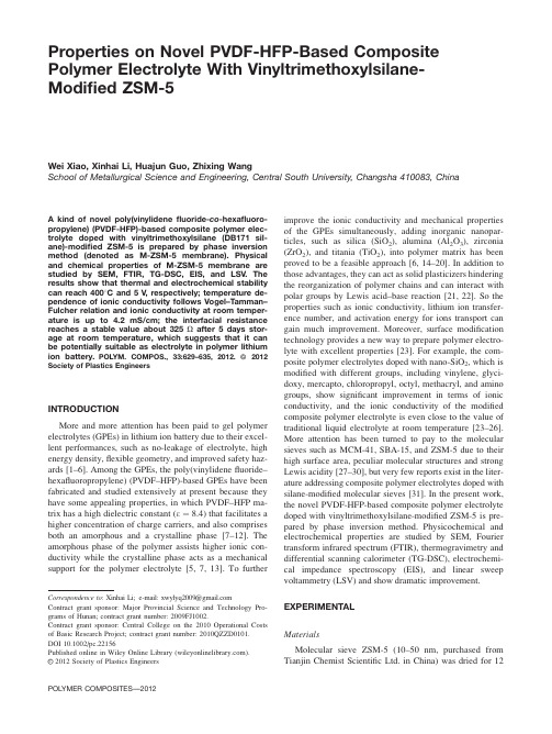
Mg2Si/Si雪崩光电二极管的设计与模拟*王傲霜 肖清泉† 陈豪 何安娜 秦铭哲 谢泉(贵州大学大数据与信息工程学院, 新型光电子材料与技术研究所, 贵阳 550025)(2020 年11 月16日收到; 2020 年12 月17日收到修改稿)Mg2Si作为一种天然丰富的环保材料, 在近红外波段吸收系数高, 应用于光电二极管中对替代市面上普遍使用的含有毒元素的红外探测器具有重要意义. 采用Silvaco软件中Atlas模块构建出以Mg2Si为吸收层的吸收层、电荷层和倍增层分离结构Mg2Si/Si雪崩光电二极管, 研究了电荷层和倍增层的厚度以及掺杂浓度对雪崩光电二极管的内部电场分布、穿通电压、击穿电压、C-V特性和瞬态响应的影响, 分析了偏置电压对I-V特性和光谱响应的影响, 得到了雪崩光电二极管初步优化后的穿通电压、击穿电压、暗电流密度、增益系数(M n)和雪崩效应后对器件电流的放大倍数(M). 当入射光波长为1.31 µm, 光功率为0.01 W/cm2时, 光电二极管的穿通电压为17.5 V, 击穿电压为50 V, 在外加偏压为47.5 V (0.95倍击穿电压)下, 器件的光谱响应在波长为1.1 µm处取得峰值25 A/W, 暗电流密度约为3.6 × 10⁻⁵ A/cm2, M n为19.6, 且M n在器件击穿时有最大值为102, M为75.4. 根据模拟计算结果, 优化了器件结构参数, 为高性能的器件结构设计和实验制备提供理论指导.关键词:SACM-APD, Mg2Si/Si异质结, 光谱响应, 增益系数PACS:85.30.–z, 73.40.Lq, 85.60.Gz, 42.60.Lh DOI: 10.7498/aps.70.202019231 引 言市面上的红外光电探测器普遍使用了铟镓砷(InGaAs)[1]、碲镉汞(HgCdTe)[2,3]材料, 这些原材料具有吸收系数高、带隙可调、增益系数高和电子迁移率高等优点[3,4], 但其含量在地壳中不多, 并且均含有重金属元素, 将其大量应用于红外光电探测器将会出现原材料匮乏, 且对环境造成的污染也不容忽视[5,6], 因此寻找其他合适的材料制备红外器件已成为解决上述问题的关键[7].Mg2Si是红外光电探测器最理想的原材料之一, 具有天然丰富、环境友好、载流子迁移率高、在近红外波段光吸收系数高[8,9]、与Si的晶格失配小(< 5%)[10,11]、与成熟的Si工艺兼容[12]、与n型Si有良好的欧姆接触[13]、高纯的单晶Mg2Si是n 型半导体[10]而掺杂银或铜后能成为p型半导体[14]等优点. 但目前对Mg2Si用于光电子器件的文献报导不多, 大多数研究组都是对其基本性质进行研究. Udono等[15]和El-Amir等[16]先后通过热扩散制作了Mg2Si光电二极管, 表明其具有良好的整流特性, 在波长为0.95—1.8 µm范围内有良好的光谱响应, 在零偏压下, 波长为1.4 µm处光谱响应达到峰值为0.014 A/W, 展示了其作为红外光电探测器的应用前景, 对替代市面上含有毒元素的红外光电探测器具有重要研究意义.为了开发基于Mg2Si薄膜的红外探测器, 此前我们研究组已经围绕Mg2Si/Si异质结光电二极管设计了pn型和pin型的器件模型[17], 所模拟的pin型器件要优于pn型器件, 光谱响应峰值为* 贵州省留学回国人员科技活动择优资助项目(批准号: [2018]09)、贵州省高层次创新型人才培养项目(批准号: [2015]4015)和贵州省研究生科研基金(批准号: [2020]035)资助的课题.† 通信作者. E-mail: qqxiao@© 2021 中国物理学会 Chinese Physical Society 0.742 A/W, 但暗电流密度略大, 约为1×10⁻⁶ A/cm2.而研究发现雪崩光电二极管(APD)具有高增益、宽带宽、响应快等[18,19]诸多优点, Nishida等[20]将吸收层和倍增层分离而提出的吸收层、电荷层和倍增层分离(SACM)结构成为当前APD普遍所采用的结构. 因此本文考虑到Mg2Si/Si异质生长的晶格失配度, 在保证Mg2Si/Si异质结能良好生长的前提下, 采用Silvaco软件中Atlas模块构建出以Mg2Si为吸收层的Mg2Si/Si SACM-APD, 为高性能的器件制备提供指导, 降低器件研制经费, 提高器件性能, 使高性能Mg2Si红外探测器件的制备成为可能, 从而解决红外探测器原材料匮乏及不环保的问题.2 SACM-APD的结构设计理论模型采用Silvaco中的Atlas模块对Mg2Si/Si异质结SACM-APD的结构进行设计. Nishida等[20]将吸收层和倍增层分离而提出的SACM型结构成为当前APD普遍所采用的结构,此结构可以通过调节电荷层的结构参数来调节器件内部场强. 本文设计的SACM-APD如图1所示, 器件衬底采用重掺杂n型Si, 衬底上生长一层n型Si作为缓冲层, 接着是弱p型掺杂的Si作为倍增层, 较高掺杂的p型Si电荷层位于倍增层与Mg2Si吸收层之间, 以调节器件内部电场分布, 最后采用较薄且掺杂浓度高的p型Mg2Si薄膜作为接触层. 为形成欧姆接触, n型Si衬底通常需要高的掺杂浓度[12].图 1 SACM-APD结构示意图Fig. 1. Schematic diagram of SACM-APD.图2为Mg2Si/Si SACM-APD的能带结构示意图, 图中建立一维的坐标系, p-Mg2Si接触层顶位置设为坐标原点, W p, W a, W c, W m, W b与W s分别为器件接触层、吸收层、电荷层、倍增层、缓冲层和衬底的厚度, 参数见表1.Energy/eVThickness/m m图 2 APD的能带结构图Fig. 2. Energy band structure diagram of the APD.表 1 APD的结构参数Table 1. Structural parameters of the APD.层名符号厚度/µm符号浓度掺杂/× 1016 cm–3金属电极层—0.1—0Mg2Si接触层W p0.15N p500Mg2Si吸收层W a0.6—4N a0.1Si电荷层W c0.1—0.3N c6—14Si倍增层W m1N m0.01—1Si缓冲层W b0.5N b100Si衬底W s 3.5N s1000物理模型中的材料参数均来自最近的文献[9, 15, 21, 22]与本研究组的测试结果, 表2为Mg2Si 与c-Si的一些基础的材料参数.表 2 模拟计算中采用的各层基本参数Table 2. The parameters of different layers in the simu-lation.参数Mg2Si c-Si[21]相对介电常数20[21]11.9电子迁移率/(cm2·V–1·S–1)550[21]1350空穴迁移率/(cm2·V–1·S–1)70[15]500材料带隙/eV0.77[9,21] 1.12导带有效态密度/cm–37.8 × 1018 2.8 × 10¹⁹价带有效态密度/cm–3 2.06 × 10¹⁹ 1.04 × 10¹⁹电子亲和力/eV 4.37[21,22] 4.05对于光电器件的模拟, 为了使仿真结果更接近实际, 材料表面折射率情况被考虑到, 吸收系数是光电器件模拟中重要的参数, 对光生载流子的产生率以及光生电流起着主导的作用, 文中Mg 2Si [9]与c-Si [23]中的吸收系数与折射率均来自于近期文献中实验测量到的, 如图3所示.1010101010106543210A b s o r p t i o n c o e f f i c i e n t /c m -1Photon energy/eVR e f r a c t i v e i n d e xWavelength/m m图 3 Mg 2Si 与c-Si 的光学特性 (a) Mg 2Si 与c-Si 的吸收系数(cm –1)与入射能量的关系; (b) Mg 2Si 与c-Si 的折射率与波长的关系Fig. 3. Optical properties of Mg 2Si and c-Si: (a) Absorption coefficient(cm –1) of the poly-Mg 2Si and c-Si; (b) refractiveIndex of the poly-Mg 2Si and c-Si.3 Mg 2Si/Si SACM-APD 的性能仿真与分析3.1 内部电场与载流子分布图4(a)给出了Mg 2Si/Si SACM-APD 在电荷层厚度为0.1 µm 时随外加电压升高的内部电场分布图. 由图4(a)可知, 当电荷层太薄时, 对器件的倍增层与吸收层的场强分布调控能力不足, 倍增层电场将会延伸至吸收层中, 即无法使倍增层与吸收层完全分离开来, 会使雪崩倍增效应在吸收层中加剧, 器件的隧穿电流增大, 影响器件性能. 如图4(b)所示, 当电荷层厚度增加为0.2 µm 时, 吸收层与倍增层分离开来, 使雪崩效应主要在倍增层中产生, 光生载流子的产生则几乎在吸收层中, 这种情况下将能显著地降低器件的暗电流, 因此电荷层厚度设置不应太薄.图5揭示了不同外加偏压下的器件内部的载流子生成率, 由图5可知, 在偏压小于20 V 时, 器件内部载流子生成率几乎只发生在倍增层中, 对应的此时暗电流增加较为平稳. 但当偏压为40 V 时,倍增层中的载流子生成率上升了两个数量级, 部分耗尽区中也存在载流子生成, 此时器件处于穿通状态. 当偏压增大至60 V 时, 倍增层中载流子生成率达到1026 cm 3·s 数量级, 电流快速增加, 器件已处于雪崩击穿状态.0123451234E l e c t r i c f i e l d /(105 V S c m -1)Thickness/m m0 V 20 V 40 V 60 V(a)01234501234E l e c t r i c f i e l d /(105 V S c m -1)Thickness/m m0 V 20 V 40 V 60 V(b)图 4 (a) 电荷层厚度为0.1 µm 时器件的电场分布; (b) 电荷层厚度为0.2 µm 时器件的电场分布Fig. 4. (a) Electric field distribution of the device with charge layer thickness of 0.1 µm; (b) electric field distribu-tion of the device with charge layer thickness of 0.2 µm.012345Thickness/m m0 V 20 V 40 V 60 VI m p a c t g e n r a t e /(c m 3S s )10241016108100图 5 Mg 2Si/Si SACM-APD 器件在不同偏压下内部的载流子生成率Fig. 5. The influence of the different Bias voltage on the carrier generation rate.图6为在外加偏压为40 V 时, 倍增层不同掺杂浓度下倍增层的电场分布关系, 在掺杂浓度为1 × 1014 cm –3, 其内部电场分布均匀, 当掺杂浓度继续增加至1 × 1015 cm –3时, 整体的电场强度增加有限, 其分布呈现出较小程度的倾斜, 继续增高掺杂浓度, 倍增层整体电场强度上升很快, 且不均匀程度加剧, 此时会导致器件产生较大的暗电流,降低器件的增益系数. 所以在器件制备中, 为保证倍增区的电场相对稳定, 倍增层的掺杂浓度一般不宜超过1 × 1015 cm –3. 另一方面接触层采用重掺杂方式, 可提高内部整体电场, 使得吸收层电场起伏变小.3.23.64.0E l e c t r i c f i e l d /(105 V S c m -1)Thickness/m m0.20.40.61T 1014 cm -34T 1014 cm -31T 1015 cm -35T 1015 cm -31T 1016 cm -3图 6 倍增层不同掺杂浓度时倍增层的电场分布Fig. 6. Electric field distribution of the multiplier layer un-der different doping concentrations.3.2 穿通电压与击穿电压穿通电压[20]和击穿电压均会受到APD 结构参数的影响, 如各层掺杂浓度、厚度等. 在模拟中,设置这些参数为变量以获得穿通电压和击穿电压的变化趋势, 对后续工艺设计具有至关重要的作用.∆(V b −V p )如图7所示, 图中上半部分呈下降趋势的四条曲线V b 为不同电荷层厚度的击穿电压, 下半部分呈上升趋势的四条曲线V p 为不同电荷层厚度下的穿通电压. 若电荷层厚度一定时, 当其掺杂浓度升高, 穿通电压呈线性上升趋势, 而击穿电压呈线性下降趋势, 且下降趋势较为明显. 当电荷层厚度为0.1 µm 时, 穿通电压随掺杂浓度的变化趋势为1.2 V/2 × 1016 cm –3, 击穿电压随掺杂浓度的变化趋势4 V/2 × 1016 cm –3, 击穿电压和穿通电压之差 随掺杂浓度升高而降低, 在掺杂浓度为6 × 1016 cm –3时, 有最大值64 V. 当厚度增加至0.25 µm 时, 穿通电压随掺杂浓度的变化趋势∆(V b −V p )∆(V b −V p )为2 V/2 × 1016 cm –3, 击穿电压随掺杂浓度的变化趋势15 V/2 × 1016 cm –3, 在掺杂浓度为6 ×1016 cm –3时, 有最大值37 V. 在设计雪崩光电二极管的结构参数时, 如果电荷层厚度设计的较薄且掺杂浓度较低, 在小偏压情况下, 器件中的吸收层会产生耗尽, 器件提前处于穿通状态. 同时电荷层对器件中倍增层的电场调控作用力度较弱, 需要外加极大的偏压才能使倍增层中形成足够大的电场产生雪崩倍增效应, 这都极大地影响器件的性能. 若选用较厚且高掺杂的电荷层时, 此时电荷层对器件倍增层与吸收层电场调控作用较强, 会使倍增层中的电场加强, 吸收层中的电场削弱, 此时需要较大的外加电压才能使器件处于穿通状态,但需要不大的外加电压就会使器件处于击穿状态.例如当电荷层厚度为0.25 µm 、掺杂浓度为1 ×1017 cm –3, 仅为3 V, 若再增加电荷层厚度与掺杂浓度时, 会导致器件中耗尽区尚未完全耗尽时就已处于击穿状态, 在器件制备过程中应极力避免此情况, 电荷层的设计要结合实际进行综合考虑.w m w m w m 当电荷层掺杂浓度为8 × 1016 cm –3、厚度为0.2 µm 时, 图8揭示了倍增层厚度 的增加对APD 穿通电压与击穿电压的影响. 如图8所示, 击穿电压随 的增大出现先减小后增大的现象, 从0.2到0.6 µm 时总体呈下降趋势, 在0.6到1.2 µm 时呈上升趋势, 在0.6 µm 时V b 取得最小值53 V,且总体呈现非线性变化规律, 而穿通电压呈线性增加, 上述变化趋势可由APD 的增益系数公式[24]来V o l t a g e /VDoping concentration/(1016 cm -3)图 7 电荷层厚度、掺杂浓度与击穿电压和穿通电压之间的关系Fig. 7. The relation between the thickness and doping con-centration of charge layer and the breakdown voltage, the punch-through voltage.解释. 若倍增区厚度太薄, 会产生较大的击穿电压与很小的穿通电压. 因此在实际制作中可适当提高倍增层厚度, 提升载流子在倍增层中碰撞电离的几率, 提高器件的增益系数.图9揭示了雪崩光电二极管中的倍增层不同掺杂浓度对器件的击穿电压与穿通电压的影响. 当倍增层掺杂浓度升高, 击穿电压逐渐下降, 且下降趋势微弱, 掺杂浓度从1 × 1014 cm –3上升至1 ×1015 cm –3时, 击穿电压仅从56 V 下降至53 V, 穿通电压则几乎没变.Doping concentration/cm -3b /Vp /V图 9 倍增层不同掺杂浓度与穿通电压和击穿电压关系Fig. 9. Breakdown voltage and penetration voltage at differ-ent doping concentration of the multiplier layer.3.3 I -V特性与光谱响应APD 的内部增益机制一般为雪崩倍増, 本工作中的电子在高电场作用下的倍增层碰撞电离的几率是随机的, 因此倍增后生成的电流分布不均匀, 雪崩光电二极管产生一个附加噪音机制, 称为倍增噪音, 是雪崩光电二极管主要的噪音来源.Si 中电子的碰撞电离系数比空穴高, 因此采用电子作为雪崩光电二极管的倍增机制. 一般由电子倍增产生的噪音F n 为[25]k 其中代表倍増区域内有效空穴与电子的离化系数的比值; M n 为增益系数, 是APD 中最基本的参数之一. 增益系数一般定义为光照下产生的电流I P 减去黑暗下的暗电流I D 之差与有效光电流I A 之比. 在计算过程中一般如下公式:如图10所示, 黑色曲线与红色曲线分别代表雪崩光电二极管在黑暗与光照下(l = 1.31 µm,光功率 = 0.01 W/cm 2)下的I-V 曲线. APD 在偏压为12 V 左右耗尽区开始逐渐向Mg 2Si 吸收层扩散, 提升了入射光被Mg 2Si 薄膜层吸收形成光生载流子的几率, 耗尽区的场强分布提高, 自由载流子越过吸收层与电荷层到达倍增层的概率升高, 暗电流会有较大幅度的提升. 当偏压为18 V 左右时吸收层被完全耗尽, 器件处于穿通状态. 随着偏压的继续增大, 此时耗尽区会向p 区与n 区延伸, 倍增层雪崩效应开始显现, 此时器件的电流增加较为平缓. 在50 V 左右时, 器件倍增层中的电子在高电场情况下雪崩碰撞离化明显, 暗电流与光电流几乎呈指数增长, 发生击穿. 当器件工作处于线性模式下(V p < V < V b ), M n 从0.75增加至最大值102,电压为0.95V b 时的M n 为19.6, 与传统的Si 基雪崩光电二极管接近. 此时器件的暗电流密度为3.6 × 10⁻⁵ A/cm 2, 该Mg 2Si/Si SACM-APD 与pn 型和pin 型Mg 2Si/Si 光电二极管相比, 具有略大的暗电流密度[17], 与目前国际上商用的红外探测器性能对比见表3, 在器件制备时, 要注意严格控制各层的参数从而控制暗电流密度.Thickness/m mb /Vp /V图 8 不同倍增层厚度时的击穿电压与穿通电压Fig. 8. Breakdown voltage and penetration voltage at differ-ent thicknesses of the multiplier layer.C u r r e n t /AVoltage/VG a i n c o e f f i c i e n t10101010101010101010图 10 APD 的I-V 特性与增益系数Fig. 10. I-V characteristics and gain coefficient of APD.表 3 模拟结果与目前国际水平对比Table 3. Comparison of simulation results with current international level.材料暗电流密度/(A·cm –2)光谱响应/(A·W –1)InGaAs 5 × 10⁻⁴[26] 1.2[26]InGaAs/InP 7 × 10⁻¹⁰[26]—HgCdTe/CdTe/Si 0.007[26]—HgCdTe/CdZnTe2.7 × 10–5[27] 1.45[27]Mg 2Si 0.04[14,16]0.014[14,16]Mg 2Si/Si-pn 6 × 10⁻⁷[17]0.32[17]Mg 2Si/Si-pin 1 × 10⁻⁶[17]0.742[17]Mg 2Si/Si-SACM3.6 × 10–525图11为外加偏置电压对APD 光谱响应的影响, 由图可知器件的光谱响应波长能扩展至1.6 µm,因此选用Mg 2Si 作为吸收层能有效地扩展Si 基APD 的光谱响应波段. 在47.5 V(0.95V b )偏压下,波长为1.1 µm 时光谱响应达到峰值, 为25 A/W,在1.31 µm 处也有较高的响应度, 所以此APD 可适用于光通信等光电设备领域中. 总体而言, 随着偏置电压的增大, APD 的光谱响应不断增强, 但其随波长的变化趋势保持了较好的一致性. 越接近击穿电压, 增强的幅度越大. 当在偏压为17.5 V 时, APD 的吸收层被完全耗尽, 器件被穿通, 此时倍增效应还未产生, 因此选取17.5 V 为器件的穿通电压.I MP 与I MD I P 与I D 若设 分别是雪崩倍增效应后的光电流与暗电流, 是未发生雪崩倍增效应的光电流与暗电流, 仿真计算时取器件穿通前光电流与暗电流之差的平均值代表倍增效应前的电流, 两者之比M 如下式所示:I MP 与I MD 上式中M 可表示雪崩效应后对电流的放大倍数. 通过先前的工作确定17.5 V 为器件的穿通电压, 取17.5 V 以前光电流与暗电流之差的平均电流为倍增前的电流, 17.5 V 以后为倍增后的电流.如图10所示, M 在偏压大于46 V 时迅速增加, 在50.8 V 时有最大值1660. 若取 之差的平均电流为倍增后的电流, 经计算此时M 为75.4, 证明该结构对电流的增益效果较好.3.4 器件的C-V 特性与开关特性C j C j C τC d C j 图12为APD 在频率为1 MHz 下的C-V 仿真曲线随倍增层厚度的变化. 当外加偏压一定时,随着倍增层厚度的增加, 器件电容减小. 当厚度一定时, 随着外加偏压的减小, 器件电容增大. 从理论上分析时, APD 中由于电极与衬底介电性产生的电容和管壳电容是由器件工艺来决定的, 在这里不做讨论, 只考虑结电容 , 可等效为pn 结处理,如果外部交流小信号频率很高时, 电容 以耗尽电容 为主, 可忽略 [28], 当外加交流偏置电压V 时得到 关系式为[28,29]由(4)式可推知, 当倍增层厚度和偏置电压变大时, 耗尽层宽度会相应展宽, 器件电容减小, 与Wavelength/m mR e s p o n s i v i t y /(A S W -1)图 11 不同的偏置电压对APD 光谱响应的影响Fig. 11. Effect of different bias voltages on the spectral re-sponse of APD.-4-2024681.21.11.0Voltage/V0.3 m m 0.6 m m 1.0 m mC a p a c i t a n c e d e n s i t y /(10-15 F S m m -1)图 12 倍增层厚度对器件电容的影响Fig. 12. The influence of the thickness of multiplication lay-er on the capacitance of the device.模拟变化结果相一致. 探测器带宽与RC 关系是呈负相关[25]:根据(5)式可知合理降低器件电容是有必要的. 当倍增区厚度为1 µm 时, 在5 V 偏置电压下,器件电容密度约为1 × 10–15 F/µm.图13为不同倍增层厚度时器件的瞬态响应曲线, 增加倍增层厚度, 对器件的响应时间影响微弱,但器件的稳态光电流却是先减小后增大, 可能是因为倍增层厚度的增加会调控器件内部场强分布, 使击穿电压出现先降低后升高的趋势. 本例中得到的瞬态响应曲线的偏压均为37 V, 因此倍增层厚度的不同导致了不同的稳态光电流.0.3 m m 0.6 m m 1.0 m m101550654321C a t h o d e c u r r e n t /(10-6 A )Transient time/(10-9 s)图 13 不同倍增层厚度时器件的瞬态响应Fig. 13. Transient response of the device for different thick-ness of the multiplication layer.4 结 论考虑到Mg 2Si/Si 异质生长的晶格失配度, 建立了Mg 2Si/Si SACM-APD 模型, 研究了电荷层和倍增层的厚度以及掺杂浓度对雪崩光电二极管的内部电场分布、穿通电压(V p )、击穿电压(V b )、C-V 特性和瞬态响应的影响, 分析了偏置电压对I-V 特性和光谱响应的影响, 得到了Mg 2Si/Si SACM-APD 初步优化后的V p , V b 、暗电流密度、增益系数(M n )和雪崩效应后对器件电流的放大倍数(M ), 为高性能的器件制备奠定了良好的基础.根据模拟结果可知: 器件的光谱响应波长能扩展至1.6 µm, 选用Mg 2Si 作为吸收层的APD 能有效地扩展Si 基APD 的光谱响应波段. 随着电荷层厚度与掺杂浓度的升高, 器件的V p 呈线性上升趋势,而V b 呈线性下降趋势, 且下降趋势较为明显, 因此电荷层能较好地调节器件内部电场分布. 当倍增层掺杂浓度大于1 × 1015 cm –3后, 倍增层电场分布出现较大程度的不均衡, 会产生较大的暗电流,因此为保证倍增区的电场相对稳定, 倍增层的掺杂浓度不宜超过1 × 1015 cm –3. 在器件结构参数优化后, SACM-APD 的V p 为17.5 V, V b 为50 V; 当偏压为47.5 V (0.95V b )时, 器件的光谱响应在波长为1.1 µm 时达到峰值25 A/W, 与先前的研究中pin 型Mg 2Si/Si 光电二极管的光谱响应峰值0.742 A/W 相比, 光谱响应得到了很大程度的提高; 暗电流密度约为3.6 × 10⁻⁵ A/cm 2, 该Mg 2Si/Si SACM-APD 与pn 型和pin 型Mg 2Si/Si 光电二极管暗电流密度1 × 10⁻⁶ A/cm 2相比, 暗电流密度略大; M n 为19.6, 且M n 在器件击穿时取得最大值为102, M 为75.4, 器件具有较好的增益效果. 在器件制备过程中, 考虑到Mg 2Si/Si 异质生长的晶格失配度, 界面态密度应控制在1 × 1011 cm –2以内, 并且可以通过在器件表面加设保护环[30]来提高器件的反向耐压性能.参考文献M o Q Y, Zhao Y L 2011 Acta Phys. Sin. 60 072902 (inChinese) [莫秋燕, 赵彦立 2011 物理学报 60 072902][1]P ark S M, Grein C H 2019 J. Electron. Mater. 48 8163[2]R ogalski A 2005 Rep. Prog. Phys. 68 2267[3]X u S J, Chua S J, Mei T, Wang X C, Zhang X H, KarunasiriG, Fan W J, Wang C H, Jiang J, Wang S, Xie X G 1998Appl. Phys. Lett. 73 3153[4]R ogalski A 2002 Infrared. Phys. Technol. 43 187[5]R ogalski A 2011 Infrared. Phys. Technol. 54 136[6]H u W D, Li Q, Chen X S, Lu W 2019 Acta Phys. Sin. 68120701 (in Chinese) [胡伟达, 李庆, 陈效双, 陆卫 2019 物理学报 68 120701][7]L aBotz R 1963 J. Electrochem. Soc. 110 127[8]K ato T, Sago Y, Fujiwara H 2011 J. Appl. Phys. 110 063723[9]B orisenko V E 2000 Semiconducting Silicides (New York:Springer) pp137−179[10]A u-Yang M Y, Cohen M L 1969 Phys. Rev. 178 1358[11]L iao Y F, Fan M H, Xie Q, Xiao Q Q, Xie J, Yu H, Wang SL, Ma X Y 2018 Appl. Surf. Sci. 403 302[12]J anega P L, McCaffrey J, Landheer D, Buchanan M, DenhoffM, Mitchel D 1988 Appl. Phys. Lett. 53 2056[13]U dono H, Tajima H, Uchikoshi M, Itakura M 2015 Jpn. J.Appl. Phys. 54 07JB06[14]U dono H, Yamanaka Y, Uchikoshi M, Isshiki M 2013 J. Phys.Chem. Solids. 74 311[15]E l-Amir A A M, Ohsawa T, Nabatame T, Ohia A, Wadaa Y,Nakamuraa M, Fua K, Shimamuraa K, Ohashia N 2019Mater. Sci. Semicond. Process. 91 222[16]C hen H, Xiao Q Q, Xie Q, Wang K, Shi J N, 2019 Mater.Rep. 33 3358 (in Chinese) [陈豪, 肖清泉, 谢泉, 王坤, 史娇娜2019 材料导报 33 3358][17]F orrest S R, Kim O K, Smith RG 1982 Appl. Phys. Lett. 4195[18]Z hang H Y, Wang L L, Wu C Y, Wang Y R, Yang L, PangH F, Liu Q L, Guo X, Tang K, Zhang Z P, Wu G 2020 Acta Phys. Sin. 69 074204 (in Chinese) [张海燕, 汪琳莉, 吴琛怡, 王煜蓉, 杨雷, 潘海峰, 刘巧莉, 郭霞, 汤凯, 张忠萍, 吴光 2020 物理学报 69 074204][19]N ishida K, Taguchi K, Matsumoto Y 1979 Appl. Phys. Lett.35 251[20]D eng Q, Wang Z, Wang S, Shao G D 2017 Sol. Energy 158654[21]S ekino K, Midonoya M, Udono H, Yamada Y Udono H 2011Phys. Procedia 11 171[22]M artin A G 2008 Sol. Energy Mater. Sol. Cells 92 1305[23]P ark C Y, Hyun K, Kang S G, Kim H M 1995 Appl. Phys.Lett. 67 3789[24]S metona S, Matukas J, Palenskis V, Olechnovicius M, A.Kaminskas K, Mallard R 2004 Proceedings of SPIE-Photonics North 2004: Optical Components and Devices Ottawa,[25]Canada, September 26–29, 2004 p834X ie T, Ye X H, Xia H, Li J Z, Zhang S J, Jiang X Y, Deng W J, Wang W J, Li Y Y, Liu W W, Li X, Li T X 2020 J.Infrared Millim. W. 39 0583 (in Chinese) [谢天, 叶新辉, 夏辉,李菊柱, 张帅君, 姜新洋, 邓伟杰, 王文静, 李玉莹, 刘伟伟, 李翔, 李天信 2020 红外与毫米波学报 39 0583][26]Y uan H, Zhang J, Kim J, Meyer C, Laquindanum J, Kimchi J, Lei J 2018 Proceedings of SPIE -Infrared Sensors, Devices,and Applications VIII San Diego, United States, August 22–23, 2018 p107660 J-1[27]W ang Y D, Chen J, Xu J D, Li X Y 2018 Infrared Phys.Technol. 89 41[28]S ze S M, K. Ng K (translated by Geng L, Wu G J) 2008Physics of Semiconductor Devices (3rd Ed.) (Xi’an: Xi’an Jiaotong University Press) pp514−523 (in Chinese) [施敏, 伍国珏 著 (耿莉, 张瑞智 译) 2008 半导体器件物理 (第3版) (西安: 西安交通大学出版社) 第514−523页][29]L ee M J, Rucker H, Choi W Y 2012 IEEE Electron Device Lett. 33 80[30]Design and simulation of Mg2Si/Si avalanche photodiode*Wang Ao -Shuang Xiao Qing -Quan † Chen Hao He An -NaQin Ming -Zhe Xie Quan(Institute of Advanced Optoelectronic Materials and Technology, College of Big Data andInformation Engineering, Guizhou University, Guiyang 550025, China)( Received 16 November 2020; revised manuscript received 17 December 2020 )AbstractInGaAs and HgCdTe materials are widely used in short wave infrared photodetectors, which contain heavy metal elements. The massive use of the heavy metal elements naturally results in their scarcity, and the nonnegligible environmental pollution. Searching for other suitable materials for infrared devices becomes a key to solving the above problems. As a kind of abundant and eco-friendly material, Mg2Si has a high absorption coefficient in the near-infrared band. Its application in infrared detector makes it possible to replace the infrared devices containing toxic elements on the market in the future. The Mg2Si/Si avalanche photodiode(APD) with separation structure of absorption layer, charge layer and multiplication layer, with Mg2Si serving as the absorption layer, is constructed by using the Atlas module in Silvaco software. The effects of the thickness and doping concentration of the charge layer and multiplier layer on the distribution of internal electric field, punch-through voltage, breakdown voltage (V b), C-V characteristics, and transient response of Mg2Si/Si SACM-APD are simulated. The effects of bias voltage on the I-V characteristics and spectral response are analyzed. The punch-through voltage, breakdown voltage, dark current density, gain coefficient (M n) and the current amplification factor (M) after avalanche effect of APD are obtained after the structure optimization. According to the simulation results, the spectral response wavelength of the device is extended to 1.6 µm, so the selection of Mg2Si as the absorption layer effectively extends the spectral response band of Si based APD. When the wavelength of incident light is 1.31 µm and the optical power is 10 mW/cm2, the obtained punch-through voltage is 17.5 V, and the breakdown voltage is 50 V. When the bias voltage is 47.5 V (0.95V b), the peak value of spectral response is 25 A/W at a wavelength of 1.1 µm, a density of dark current is about 3.6 × 10⁻⁵ A/cm2, a multiplication factor M n is 19.6, and M n achieves a maximum value of 102 when the device is broken down. Meanwhile, the current amplification factor M after avalanche effect is 75.4, and the current gain effect of the SACM structure is obvious. The peak value of spectral response for the pin-type photodiode in the previous study is only 0.742 A/W. Comparing with the pin-type photodiode, the spectral response of Mg2Si/Si SACM-APD is greatly improved. In this work, the structure parameters of the device are optimized, which lays a nice foundation for fabricating the high-performance devices.Keywords: SACM-APD, Mg2Si/Si heterojunction, spectral response, gain coefficientPACS: 85.30.–z, 73.40.Lq, 85.60.Gz, 42.60.Lh DOI: 10.7498/aps.70.20201923* Project supported by the Foundation for Sci-tech Activities for the Overseas Chinese Returnees in Guizhou Province, China (Grant No. [2018]09), the High-level Creative Talent Training Program in Guizhou Province of China (Grant No.[2015]4015), and the Graduate Research Fund in Guizhou Province of China (Grant No. [2020]035).† Corresponding author. E-mail: qqxiao@。
polymer composite
Properties on Novel PVDF-HFP-Based Composite Polymer Electrolyte With Vinyltrimethoxylsilane-Modified ZSM-5Wei Xiao,Xinhai Li,Huajun Guo,Zhixing WangSchool of Metallurgical Science and Engineering,Central South University,Changsha410083,ChinaA kind of novel poly(vinylidenefluoride-co-hexafluoro-propylene)(PVDF-HFP)-based composite polymer elec-trolyte doped with vinyltrimethoxylsilane(DB171sil-ane)-modified ZSM-5is prepared by phase inversion method(denoted as M-ZSM-5membrane).Physical and chemical properties of M-ZSM-5membrane are studied by SEM,FTIR,TG-DSC,EIS,and LSV.The results show that thermal and electrochemical stability can reach4008C and5V,respectively;temperature de-pendence of ionic conductivity follows Vogel–Tamman–Fulcher relation and ionic conductivity at room temper-ature is up to 4.2mS/cm;the interfacial resistance reaches a stable value about325O after5days stor-age at room temperature,which suggests that it can be potentially suitable as electrolyte in polymer lithium ion POS.,33:629–635,2012.ª2012 Society of Plastics EngineersINTRODUCTIONMore and more attention has been paid to gel polymer electrolytes(GPEs)in lithium ion battery due to their excel-lent performances,such as no-leakage of electrolyte,high energy density,flexible geometry,and improved safety haz-ards[1–6].Among the GPEs,the poly(vinylidenefluoride–hexafluoropropylene)(PVDF–HFP)-based GPEs have been fabricated and studied extensively at present because they have some appealing properties,in which PVDF–HFP ma-trix has a high dielectric constant(e¼8.4)that facilitates a higher concentration of charge carriers,and also comprises both an amorphous and a crystalline phase[7–12].The amorphous phase of the polymer assists higher ionic con-ductivity while the crystalline phase acts as a mechanical support for the polymer electrolyte[5,7,13].To further improve the ionic conductivity and mechanical properties of the GPEs simultaneously,adding inorganic nanopar-ticles,such as silica(SiO2),alumina(Al2O3),zirconia (ZrO2),and titania(TiO2),into polymer matrix has been proved to be a feasible approach[6,14–20].In addition to those advantages,they can act as solid plasticizers hindering the reorganization of polymer chains and can interact with polar groups by Lewis acid–base reaction[21,22].So the properties such as ionic conductivity,lithium ion transfer-ence number,and activation energy for ions transport can gain much improvement.Moreover,surface modification technology provides a new way to prepare polymer electro-lyte with excellent properties[23].For example,the com-posite polymer electrolytes doped with nano-SiO2,which is modified with different groups,including vinylene,glyci-doxy,mercapto,chloropropyl,octyl,methacryl,and amino groups,show significant improvement in terms of ionic conductivity,and the ionic conductivity of the modified composite polymer electrolyte is even close to the value of traditional liquid electrolyte at room temperature[23–26]. More attention has been turned to pay to the molecular sieves such as MCM-41,SBA-15,and ZSM-5due to their high surface area,peculiar molecular structures and strong Lewis acidity[27–30],but very few reports exist in the liter-ature addressing composite polymer electrolytes doped with silane-modified molecular sieves[31].In the present work, the novel PVDF-HFP-based composite polymer electrolyte doped with vinyltrimethoxylsilane-modified ZSM-5is pre-pared by phase inversion method.Physicochemical and electrochemical properties are studied by SEM,Fourier transform infrared spectrum(FTIR),thermogravimetry and differential scanning calorimeter(TG-DSC),electrochemi-cal impedance spectroscopy(EIS),and linear sweep voltammetry(LSV)and show dramatic improvement. EXPERIMENTALMaterialsMolecular sieve ZSM-5(10–50nm,purchased from Tianjin Chemist Scientific Ltd.in China)was dried for12Correspondence to:Xinhai Li;e-mail:xwylyq2009@Contract grant sponsor:Major Provincial Science and Technology Pro-grams of Hunan;contract grant number:2009FJ1002.Contract grant sponsor:Central College on the2010Operational Costs of Basic Research Project;contract grant number:2010QZZD0101.DOI10.1002/pc.22156Published online in Wiley Online Library().V C2012Society of Plastics EngineersPOLYMER COMPOSITES—-2012h at1208C prior to use.Poly(vinylidenefluoride-co-hexa-fluoropropylene)(PVDF-HFP,Atofina,Kynar Flex,12 wt%HFP)was used as polymer matrix in the experiment and dried under vacuum for12h at808C prior to use. Analytical grade N,N-dimethylformamide(DMF)and poly(ethylene glycol)with low molecular weight of200 (PEG-200)were directly used as solvent and pore-forming agent,respectively,without further purification. Preparation of Silane-Modified Molecular SieveA certain amount of molecular sieve ZSM-5was added into5%DB171silane–ethanol mixed solution(5:95,v/v) with continuous vigorous stirring for48h at408C,then the above homogeneous solution was centrifuged at 15,000rpm and dried in vacuum at1008C for24h to fur-ther remove residual organic solvents.For the sake of convenience,the modified ZSM-5is denoted as M-ZSM-5in the following exposition.Preparation of Polymer ElectrolyteA certain content of as-prepared M-ZSM-5was dis-persed in DMF solution,and a certain mass of PVDF-HFP and PEG-200were added to the well-dispersed solu-tion with continuous stirring for3–4h at408C to form homogeneous and viscous slurry,in which the mass ratio between the M-ZSM-5and the PVDF-HFP is about1:10. The casting solution was cast onto a glass plate with a doctor blade to form the wet membrane after leaving still for2h at408C,followed by being immersed into deion-ized water at room temperature for12h to obtain the polymer electrolyte membrane.The resulting membranes were further dried under vacuum at608C for24h to remove the residual solvent.The membranes prepared were about120–150l m in thickness.Then the desirable polymer electrolytes were prepared by immersing the as-prepared membranes into the1.0M LiPF6-ethylene car-bonate(EC)/dimethyl carbonate(DMC)/ethylmethyl car-bonate(EMC)(1:1:1,w/w/w)liquid electrolyte solution (provided by Dongguan Shanshan Battery Materials Co. Ltd.in China)at room temperature for1h,which was carried out in a dry-box under argon gas atmosphere to avoid moisture.The PVDF-HFP-based composite polymer electrolytes modified with and without ZSM-5were also prepared in our work as control samples according to the above-mentioned experimental steps.Properties CharacterizationA scanning electron microscope(SEM,JSM6301F) with an accelerating voltage of20kV was used to exam-ine the membrane surface sputter coated with gold under vacuum atmosphere.The PEPARAGN1000instrument with a wave number resolution of2cm21in the fre-quency of4000to400cm21was used to record the FTIR of M-ZSM-5.TG-DSC measurements were carried out on a Perkin-Elmer Pyris-1analyzer.The measurements were performed at a heating rate of108C/min from20to 4008C.Aflow of nitrogen gas was maintained over the perforated pan to avoid any contact with atmospheric moisture.The weights of samples were maintained in the range of12–15mg and an empty aluminum pan was used as a reference.The liquid electrolyte uptake(A)was cal-culated using the following relation Eq.1,where,w1and w0are the weights of the wet and dry membranes,respec-tively.A%¼w1Àw0w03100%(1)The ionic conductivity of the composite polymer elec-trolyte was determined by EIS.The as-prepared electro-lyte membranes were sandwiched between two stainless steel(SS)blocking electrodes to form the SS/composite polymer electrolyte/SS model cells.The EIS tests were measured over an AC oscillation10mV frequency range of1to105Hz at various temperatures(293–363K,the cells were thermostated during measurements)using a CHI660b frequency response analyzer(Shanghai Chen-hua,China).Electrochemical stability window of the polymer electrolyte was determined by running LSV in three-electrode cell using stainless steel as the blocking working electrode,lithium as both the counter,and the reference electrode and polymer electrolyte as the electro-lyte.The LSV tests were carried out using the same sys-tem as those in EIS at a scan rate of5mV/s.In addition, the interfacial stability was studied by investigating the resistance change with different storage times of the blocking model cell Li/composite polymer electrolyte/Li.RESULTS AND DISCUSSIONSurface Morphology AnalysisFigure1presents SEM images of three kinds of differ-ent polymer electrolyte membranes with different adulter-ants.It can be obviously seen that adding molecular sieve into polymer matrix plays a major role in the surface morphology of fabricating polymer electrolyte mem-branes,no matter molecular sieve is modified with DB171silane or pared with Fig.1A,the size and the amount of micro-pores on the surface and inner decreases gradually and increases distinctly in Fig.1B and C,respectively,which may be partly attributed to the Lewis acid–base interaction between polymer matrix PVDF-HFP and molecular sieve,partly to molecular sieve as a cross-linking center during recrystallization of PVDF-HFP.On one hand,with molecular sieves added into polymer matrix,the inner-layer has more micropores and demonstrates better connectivity,which can further promote more electrolyte entrapment ratio;on the other hand,the more uniform surface morphology demonstrated in Fig.1C implies it has best compatibility between the630POLYMER COMPOSITES—-2012DOI10.1002/pcpolymer matrix and electrode,which can be well con-firmed in the following experiments.It can be seen that M-ZSM-5modified PVDF-HFP membrane not only shows most uniform surface morphology,but also presents most plentiful interconnected micropores.FTIR Analysis ResultsThe direct evidence for the reaction mechanism is pro-vided by FTIR recorded for the DB171and M-ZSM-5showed in Fig.2.The CH 3asymmetric stretching vibra-tion occurs at 2,975–2,950cm 21while the CH 2absorp-tion occurs at about 2,930cm 21.The symmetric CH 3vibration occurs at 2,885–2,865cm 21while the CH 2absorption occurs at about 2,870–2,840cm 21.The absorption bands appearing at 1,193,1,090,1,010,and 968cm 21are ascribed to IR vibrating absorption of ÀÀSi ÀÀO ÀÀCH 3bonds,and the 1,600–1,650cm 21is to C ¼¼C stretching absorption in the IR spectrum of DB171[32].A problem worthy to be pointed out is that the cor-responding band showing red shift observed at 945–1,100cm 21is ascribed to IR vibrating absorption of ÀÀSi ÀÀO ÀÀSi bonds,and the 1,600–1,650cm 21represent-ing C ¼¼C stretching absorption becomes weak in the of the spectrum of DB171-modified ZSM-5,which can be explained that silanol (Si ÀÀOH)from hydrolysis of DB171silane interacts with free hydroxyl (ÀÀOH)on the surface of the molecular sieve ZSM-5.The distinct differ-ences between the mentioned spectra indicate that molec-ular sieve is successfully modified by DB171silane.The two IR absorption peaks near 3,428and 1,639cm 21in Fig.2may be assigned to the presence of the oxygen–hydrogen single bond (O ÀÀH)from the samples contain-ing absorbable impurity water [24,25].Thermal and Electrochemical StabilityThermal and electrochemical stability are considered as the most important two factors in practicalapplicationsFIG.1.SEM images of different polymer electrolyte membranes [(A)PVDF-HFP membrane,(B)ZSM-5modified PVDF-HFP membrane,and (C)M-ZSM-5modified PVDF-HFPmembrane].FIG.2.FTIR spectra of DB171and DB171modified ZSM-5.[Color figure can be viewed in the online issue,which is available at .]DOI 10.1002/pcPOLYMER COMPOSITES—-2012631of polymer lithium ion battery.Figure 3presents the TG-DSC plots of polymer electrolyte membranes prepared by phase inversion method.Obviously,Fig.3A about the TG plots reveals that the pure PVDF-HFP electrolyte mem-brane is inferior to the ZSM and M-ZSM modified mem-brane in term of thermal stability,and the thermal stabil-ity of the membrane with M-ZSM-5can even reach 4008C with little decomposition,which can well meet the practical demands about the thermal property of lithium ion battery.Fig.3B shows the DSC plots of the three kinds of membranes.The crystallinity of the membranes can be calculated according to the following relation x %¼D H f /D H H mf from the DSC curves,where,D H Hmf is the standard enthalpy of fusion of pure PVDF,104.7J/g,and D H f is enthalpy of fusion of the PVDF-HFP-based poly-mer electrolyte membrane [10,33,34].The crystallinity of the membranes with the uptake ratio and ionic conduc-tivity at room temperature is listed in the Table 1.It is obviously seen that the values of uptake ratio and ionic conductivity increase with decreasing of the crystal-linity,indicating that molecular sieve plays a critical role in properties of the electrolyte membrane,which is ac-cordance with the above experimental results.The effects of the M-ZSM-5to enhance uptake ratio and ionic con-ductivity at room temperature may be due to abundant interconnected micro-pores in the polymer electrolyte membranes and interfacial reaction between the polymer matrix and molecular sieves.The plots of electrochemical stability window about the three kinds of electrolyte membranes at room temper-ature are demonstrated in pared with the three curves,the M-ZSM-5membrane displays the highest electrochemical stability window about 5V,which can meet practical applications requirements and implies that the M-ZSM-5plays a positive role in term of electro-chemical stability.Based on both excellent thermal and electrochemical stability,the M-ZSM-5membrane would be used as the most promising polymer electrolyte mem-brane candidate in the rechargeable polymer lithium ion battery in the future.Ionic ConductivityThe effect of M-ZSM-5on the ionic conductivity of polymer electrolyte membrane is further investigated by temperature-dependent ionic conductivity.As demon-strated in Fig.5,the ionic conductivity increases with temperature increase and the ionic conductivity of the membranes doped with molecular sieve is higher thantheFIG.3.Plots of TG (A)and DSC (B)about three kinds of polymer electrolyte membranes by phase inversion method.[Color figure can be viewed in the online issue,which is available at .]TABLE 1.Results of crystallinity,ionic conductivity,and uptake ratio about the three kinds of polymer electrolyte membranes.Crystallinity(/%)Ionic conductivity/(mS/cm)Uptake ratio (%)PVDF-HFP membrane 100.0 2.01276.52ZSM-5doped PVDF-HFP membrane50.02 3.64792.99M-ZSM-5doped PVDF-HFP membrane31.264.23598.21FIG.4.Results of LSV about the three kinds of polymer electrolyte membranes.[Color figure can be viewed in the online issue,which is available at .]632POLYMER COMPOSITES—-2012DOI 10.1002/pcpure PVDF-HFP membrane,whether it is modified by sil-ane or not,which suggests that increase temperature low-ering the activation energy for the ions transfer between the micropores in the polymer matrix can improve ionic conductivity and molecular sieves with their unique mole-cule space structure not only can provide more passage-ways for the ionic migration,but also as Lewis acid inter-act with polymer matrix to decrease the crystallinity degree for forming more amorphous areas.Furthermore,the ionic conductivity is not related linearly to the recip-rocal temperature,which is different from the reported composite polymer electrolyte doped by some other inor-ganic fillers and maybe obeys the Vogel–Tamman–Fulcher (VTF)relation [35,36].As the temperature increases,the polymer can expand easily and produce free volume.In other words,as temperature increases,the free volume increases.The resulting conductivity,represented by the overall mobility of ions and the polymer,is deter-mined by the free volume around the polymer chains,which leads to an increase in ion mobility andsegmentalFIG.5.Temperature dependence of ionic conductivity of the three kinds of different polymer electrolyte membranes.[Color figure can be viewed in the online issue,which is available at wileyonlinelibrary.com.]FIG.6.Nyquist plots of three kinds of Li/as-prepared electrolyte/Li cells with various times [(A)Pure PVDF-HFP membrane;(B)ZSM-5modified PVDF-HFP membrane;and (C)M-ZSM-5modified PVDF-HFP membrane].[Color figure can be viewed in the online issue,which is available at .]DOI 10.1002/pc POLYMER COMPOSITES—-2012633mobility that will assist ion transport and virtually com-pensate for the retarding effect of the ion clouds[36]. Interfacial PropertiesInterfacial compatibility between the polymer electro-lyte and the electrode is another important factor to ensure an acceptable performance in practical applica-tions.In the polymer electrolyte system,the passive layer between the electrode and the electrolytes grows with the time,but the uncontrolled layer plays a vital role in prac-tical applications[8].To understand the interfacial stabil-ity between electrode and electrolyte membranes,Nyquist plots of three kinds of Li/as-prepared electrolyte/Li sym-metric cells at open circle are monitored with various times.It is quite obvious from Fig.6that the resistances R i of electrolyte membranes modified by molecular sieves reach a stable value of730O(ZSM-5modified mem-brane)and325O(M-ZSM-5modified membrane)respec-tively after5days storage,however,the resistance R i of the pure PVDF-HFP membrane presents the tendency to keep growing with time under the same conditions.The results indicate that,on one hand,the passivefilm forms between the electrolyte and electrode at the beginning and reaches a stable value when adding the molecular sieve ZSM-5into the polymer matrix,thus the membranes modified by ZSM-5present lower resistances and exhibit better compatibility with the electrode[22];on the other hand,the addition of the ZSM-5can trap any impurities such as water and trace organic solvent,inhibiting the de-structive reaction on the electrode,which can improve the compatibility between the electrode and electrolyte mem-brane[10,37,38].Moreover,the M-ZSM-5modified membrane shows the best compatibility among these membranes,in the view of the authors,which can be attributed to the special surface reaction activity groups formed during the reaction of ZSM-5modified by DB171 silane.And the research on the reaction and ionic conduc-tion mechanisms about the novel polymer electrolyte are in progress in our group.CONCLUSIONSThis work introduces preparation and performances of the novel PVDF-HFP-based polymer electrolyte with DB171-modified molecular sieve ZSM-5.The practical applications such as high ionic conductivity,excellent thermal and electrochemical stability and good interfacial properties with electrode of the novel M-ZSM-5electro-lyte ensure it as the most promising polymer electrolyte for the new rechargeable lithium ion battery. REFERENCES1.F.Croce,S.Sacchetti,and B.Scrosati,J.Power Sources,162,685(2006).2.A.Manuel Stephan,Eur.Polym.J.,42,21(2006).3.J.Y.Song,Y.Y.Wang,and C.C.Wan,J.Power Sources,77,183(1999).4.V.Di Noto,vina,G.A.Giffin,E.Negro,and B.Scro-sati,Electrochim.Acta,57,4(2011).5.N.H.Idris,M.M.Rahman,J.Z.Wang,and H.K.Liu,J.Power Sources,201,294(2012).6.P.Zhang,L.C.Yang,L.L.Li,M.L.Ding,Y.P.Wu,and R.Holze,J.Memb.Sci.,379,80(2011).7.G.B.Appetecchi, F.Croce,and B.Scrosati,Electrochim.Acta,40,991(1995).8.Z.Ren,Y.Liu,K.Sun,X.Zhou,and N.Zhang,Electro-chim.Acta,54,1888(2009).9.Q.Xiao,X.Wang,W.Li,Z.Li,T.Zhang,and H.Zhang,J.Memb Sci.,334,117(2009).10.D.Saikia,H.Y.Wu,Y.C.Pan,C.P.Lin,K.P.Huang,K.N.Chen,G.T.K.Fey,and H.M.Kao,J.Power Sources,196, 2826(2011).11.A.Zalewska,M.Walkowiak,L.Niedzicki,T.Jesionowski,and ngwald,Electrochim.Acta,55,1308(2010).12.S.Ferrari, E.Quartarone,P.Mustarelli, A.Magistris,M.Fagnoni,S.Protti,C.Gerbaldi,and A.Spinella,J.Power Sources,195,559(2010).13.R.Miao,B.Liu,Z.Zhu,Y.Liu,J.Li,X.Wang,and Q.Li,J.Power Sources,184,420(2008).14.K.M.Kim,N.G.Park,K.S.Ryu,and S.H.Chang,Polymer,43,3951(2002).15.K.M.Kim,N.G.Park,K.S.Ryu,and S.H.Chang,Electro-chim.Acta,51,5636(2006).16.M.Caillon-Caravanier,B.Claude-Montigny,D.Lemordant,and G.Bosser,J.Power Sources,107,125(2002).17.P.Raghavan,J.W.Choi,J.H.Ahn,G.Cheruvally,G.S.Chauhan,H.J.Ahn,and C.Nah,J.Power Sources,184,437 (2008).18.P.Raghavan,X.Zhao,J.K.Kim,J.Manuel,G.S.Chauhan,J.H.Ahn,and C.Nah,Electrochim.Acta,54,228(2008). 19.X.L.Wang,Q.Cai,L.Z.Fan,T.Hua,Y.H.Lin,and C.W.Nan,Electrochim.Acta,53,8001(2008).20.Y.J.Kim, C.H.Ahn,M.B.Lee,and M.S.Choi,Mater.Chem.Phys.,127,137(2011).21.Z.Chen,L.Z.Zhang,R.West,and K.Amine,Electrochim.Acta,53,3262(2008).lia,N.Yoshimoto,M.Egashira,and M.Morita,J.Power Sources,194,531(2009).23.M.Walkowiak,D.Waszak,G.Schroeder,and B.Gierczyk,mun.,10,1676(2008).24.M.Walkowiak, A.Zalewska,T.Jesionowski,and M.Pokora,J.Power Sources,173,721(2007).25.M.Walkowiak,A.Zalewska,T.Jesionowski,D.Waszak,and B.Czajka,J.Power Sources,159,449(2006).26.C.Shen,J.Wang,Z.Tang,H.Wang,H.Lian,J.Zhang,and C.N.Cao,Electrochim.Acta,54,3490(2009).27.J.Xi,X.Qiu,and L.Chen,Solid State Ionics,177,709(2006).28.J.Xi,X.Qiu,X.Ma,M.Cui,J.Yang,X.Tang,W.Zhu,and L.Chen,Solid State Ionics,176,1249(2005).29.J.Xi,X.Qiu,J.Wang,Y.Bai,W.Zhu,and L.Chen,J.Power Sources,158,627(2006).634POLYMER COMPOSITES—-2012DOI10.1002/pc30.J.Xi and X.Tang,Electrochim.Acta,51,4765(2006).31.X.L.Wang,A.Mei,M.Li,Y.Lin,and C.W.Nan,SolidState Ionics,177,1287(2006).32.P.Verma,P.Maire,and P.Nova´k,Electrochim.Acta,55,6332(2010).33.B.A.Rozenberg and R.Tenne,Prog.Polym.Sci.,33,40(2008).34.M.J.Reddy and P.P.Chu,J.Power Sources,135,1(2004).35.S.Bandyopadhyay,R.F.Marzke,R.K.Singh,and N.New-man,Solid State Ionics,181,1727(2010).36.Y.Tominaga,T.Shimomura,and M.Nakamura,Polymer,51,4295(2010).37.J.Xi and X.Tang,Electrochim.Acta,50,5293(2005).38.Y.X.Jiang,Z.F.Chen,Q.C.Zhuang,J.M.Xu,Q.F.Dong,L.Huang,and S.G.Sun,J.Power Sources,160,1320 (2006).DOI10.1002/pc POLYMER COMPOSITES—-2012635。
吹响“等电子体”的集结号

典 型 考 题 :2 0 ( 0 7年 北 京 瑾 综 第 2 6题 ) 周 期 元 短
素 的 单 质 x、 、 在 通 常 状 况 下 均 为 气 态 , 有 下 列 Y z 并 转 化 关 系 ( 应 条 件 略 去 ) 反 :
已 知 :a 常 见 双 原 子 单 质 分 子 中 , 分 子 含 共 价 . X
种 投 料 方 式 相 等 即 可 达 到 等 效 平 衡 若 - 不 等 于 3 z , 则 须 满 足 第 2种 投 料 方 式 通 过 可 逆 反 应 的 化 学 汁 量 数 比换 算 成 平 衡 式 左 右 两 边 同 一 边 物 质 的 物 质 的 量 与 第 1种 投 料 方 式 完 全 相 等 , 能 使 二 平 衡 等 效 。 才
人 人 好 公 , 天 下 太平 ; 人 营私 , 天 下 大 乱 . 则 人 则 一
H Ci 、H 2 S、 PH 3 Si 4 F2 H 2 、 C2 6、CH 3 H 、 、 l 、 、 O2 H O
小 , 到 平 衡 状 态 时 转 化 为 状 态 丙 . 设 乙 中 的 活 塞 达 假 不 移 动 由 于 甲 、 2 个 容 器 的 体 积 、 度 相 同 , 到 乙 温 达 平 衡 时 甲 、 两 容 器 中 存 在 的 平 衡 是 等 效 平 衡 , 中 乙 其 S O 的 转 化 率 也 相 等 . 于 乙 和 丙 2 个 状 态 , 中 压 对 乙 强小 于丙 中压强 , 此丙 中 S 因 O 转 化 率 大 于 乙 中 S Oz
键 最 多
b 甲分 子 中含 有 1 个电子 , 分 子 含 有 1 . 0 乙 8个 电 子 。
( ) 的 电子 式 是 1X .
() 验室 可用 下 图所示装 置 ( 少 收集 装 置 , 2实 缺 夹
固体化学复习题及答案

第一章绪论1、固体化学的研究内容是什么?基本内容包括:固体物质的合成,固体的组成和结构,固相中的化学反应,固体中的缺陷,固体表面化学,固体的性质与新材料等。
固体化学主要是研究固体物质(包括材料)的合成、反应、组成和性能及相关现象、规律和原因的科学。
固体化学的研究内容十分广泛。
它与固体物理及其他许多学科相互交叉渗透,因此很难给出明确的,全面的研究范围。
它着重于研究固态物质(包括单晶、多晶、玻璃、陶瓷、薄膜、超微粒子等)的合成、反应、组成、结构和各种宏观和微观性质。
2、假如你是从事无机材料方面的研究者,你的研究成果可以在哪些国内外期刊上投稿,试列举出其中的20种期刊。
《中国稀土学报》《功能材料》《无机材料学报》《无机化学学报》《人工晶体学学报》《硅酸盐通报》《材料科学与工艺》《SCI》《材料科学技术学报(英文版)》《材料工程》《材料导报》《纳米科技》《Chemistry of Materials》《Crystal Growth & Design》《Inorganic Chemistry》《ACS Nano》《NANO letter》《Solar energy materials and solar cells》《Rare Earth Bulletin 》《Journal of Applied Crystallography 》《Journal of the Energy Institute 》《半导体学报》《玻璃与搪瓷》《无机硅化合物》《材料研究学报》;(10)《crystal growth and disign》;(11)《internatianal journal of inorganic materials》;(12)《inorganic materials 》;(13)《crystal research and techonolgy》;(14);《journal of crystal growth 》;(15)《inorganic chemistry》;(16)《advanced founctional materials》;(17)《chemistry of materials》;(18)《japanese new materials》;(19)《journal of materials chemistry》;(20)《advanced materials》。
二氧化锰-三维结构石墨烯电极材料制备及电化学性能共3篇

二氧化锰-三维结构石墨烯电极材料制备及电化学性能共3篇二氧化锰/三维结构石墨烯电极材料制备及电化学性能1二氧化锰/三维结构石墨烯电极材料制备及电化学性能随着能源需求的不断增长和环境问题的日益突出,新型高性能电化学储能设备受到越来越广泛的关注。
二氧化锰/三维结构石墨烯电极材料作为一种新型的电化学储能材料,具有较高的比电容和循环性能,在超级电容器和锂离子电池中都有广泛的应用。
本文主要介绍二氧化锰/三维结构石墨烯电极材料的制备与电化学性能。
一、制备方法二氧化锰/三维结构石墨烯电极材料的制备一般采用两步法,首先制备石墨烯泡沫材料,再利用化学气相沉积技术将二氧化锰负载在石墨烯泡沫材料表面,最终得到二氧化锰/三维结构石墨烯电极材料。
1. 制备石墨烯泡沫材料制备石墨烯泡沫材料的方法有多种,如化学气相沉积法、物理气相沉积法、化学氧化还原法等。
本文介绍一种干法化学剥离法制备石墨烯泡沫材料的方法。
将天然石墨在高温下处理,使其表面产生氧化物,然后将氧化后的天然石墨和聚乙烯醇溶液混合,并通过超声波剥离得到石墨烯泡沫材料。
最后将石墨烯泡沫材料热处理,得到具有三维结构的石墨烯泡沫材料。
2. 负载二氧化锰将制备好的石墨烯泡沫材料浸泡在含有二氧化锰前体溶液的乙醇中,然后通过化学气相沉积技术将二氧化锰沉积在石墨烯泡沫材料表面。
最终得到二氧化锰/三维结构石墨烯电极材料。
二、电化学性能二氧化锰/三维结构石墨烯电极材料的电化学性能一般通过循环伏安法、电化学阻抗谱等测试手段进行测试。
1. 循环伏安法测定循环伏安法是一种常用的电化学测试方法,可以用于测试电化学反应的物理化学特性和电化学反应动力学特性。
将测试样品放置于电极中,在特定电位范围内进行循环伏安扫描,记录扫描图像。
通过扫描图像可以获得电极的片儿式容量、比电容、电化学反应动力学特性等数据。
2. 电化学阻抗谱测试电化学阻抗谱测试是一种可以获得电极电化学行为信息的测试方法。
将测试样品放置于电极中,施加一定的交流电压,记录阻抗谱。
《无机化学》 高教版 课后答案
11-1用氧化数法配平下列方程式。
(1)KClO3→KClO4+KCl(2)Ca5(PO4)F+C+SiO2→CaSiO3+CaF2+P4+CO(3)NaNO2+NH4Cl→N2+NaCl+H2O(4)K2Cr2O7+FeSO4+H2SO4→Cr2(SO4)3+Fe2(SO4)3+K2SO4+H2O(5)CsCl+Ca→CaCl2+Cs↑11-2 将下列水溶液化学反应的方程式先改写为离子方程式,然后分解为两个半反应式(答案见附表电极电势表):(1)2H2O2=2H2O+O2(2)Cl2+2H2O=HCl+HClO(3)3Cl2+6KOH=KClO3+5KC+3H2O(4)2KMnO4+10FeSO4+8H2SO4=K2SO4+5Fe2(SO4)3+5MnSO4+8H2O(5)K2Cr2O7+3H2O2+4H2SO4= K2SO4+Cr2(SO4)3+3O2+7H2O11-3 用半反应法(离子-电子法)配平下列方程式:(1)K2Cr2O7+H2S+H2SO4→K2SO4+Cr2(SO4)3+S+H2O (2)MnO42-+H2O2→O2+Mn2-(酸性溶液)(3)Zn+NO3-+OH-→NH3+Zn(OH)4-(4)Cr(OH) 42-+H2O2→CrO 42-(5)Hg+NO3-+H+→Hg22++NO11-4将下列反应设计成原电池,用标准电极电势判断标准下电池的正极和负极,电子传递的方向,正极和负极的电极反应,电池的电动势,写出电池符号。
(1)Zn+2Ag+= Zn2++2Ag g(2)2Fe3++Fe+=3 Fe2+(3)Zn+2H+= Zn2++H2(4)H2+Cl2=2HCl(5)3I2+6KOH=KIO3+5KI+3H2O11-5 写出下列各对半反应组成的原电池的电极反应电池符号,并计算标准电动势。
(1)Fe3++е-= Fe2+;I2+2е-=2I-(2)Cu2++I-+е-= CuI2; I2+2е-=2I-(3)Zn2++2е-= Zn;2H++2е-=H2(4)Cu2++2е-= Cu;2H++2е-=H2(5)O2+2H2O+4е-=4OH-;2H2O+2е-= H2+2OH-11-6 以标准电极电势举例来说明以下说法并非一般规律:元素的氧化态越高,氧化性就越强。
2012年西安交通大学本科生科研训练和实践创新基金项目结题验收结果

王威、胡志勇、轩杨、李卓强
王晶
合格
2012040
机械学院
利用细胞打印技术体外构建三维平滑肌微组织
刘俊聪
黄熠文
徐峰
合格
2012068
机械学院
节能汽车壳体设计及制造
汪洋
丁宝庆、丁文朝、高飞、于罗钦
王晶
合格
2012037
机械学院
倾转三涵道风扇多功能垂直起降飞行器
徐廷中
杨亚军、金博龙、陈立功、姚团结
赵立波、张安峰
孙勍铉
曹旭、王来升、夏广辉、俞亦钊
王江峰
优秀
2012020
电信学院
3+1式直升机设计及对其摄像等功能的实现
张辉
万日栋、石勇义、张弛、段泽能
杜清河
优秀
2012005
电信学院
基于CAN总线的多电机智能控制系统
董奭
杨志宇、谢磊、杨昂、吴彝丹
冯祖仁
优秀
2012006
电信学院
电磁诱导透明光开关及路由器
封玮康
黄高坪、元佳敏
苏旭
秦远智、张峰、邵栋
李景银
合格
2012058
能动学院
滤涂工艺制备基于共离子传导复相电解质低温固体氧化物燃料电池的研究
洪海峰
王峰、朱旭东
黄建兵
合格
2012002
电气学院
基于激光雷达的目标识别与随动系统研究
孙力
李卓强、胡志勇、吴彝丹、魏潇然
牟轩沁
合格
2012007
电信学院
自平衡小车的研究与制作
李维启
徐希楠、刘峰、程思婧、王映周
樊亚萍
合格
2012090
人文学院
实验一溶解热的测定

实验⼀溶解热的测定实验⼀溶解热的测定⼀、⽬的1、了解电热补偿法测定热效应的基本原理及仪器使⽤。
2、测定硝酸钾在⽔中的积分溶解热,并⽤作图法求得其微分稀释热、积分稀释热和微分溶解热。
3、初步了解计算机采集处理实验数据、控制化学实验的⽅法和途径。
⼆、基本原理1、物质溶解于溶剂过程的热效应称为溶解热。
它有积分(或变浓)溶解热和微分(或定浓)溶解热两种。
前者是1 mol 溶质溶解在n 0 mol 溶剂中时所产⽣的热效应,以Q s 表⽰。
后者是1 mol 溶质溶解在⽆限量某⼀定浓度溶液中时所产⽣的热效应,即0,,s T p n Q n。
溶剂加到溶液中使之稀释时所产⽣的热效应称为稀释热。
它也有积分(或变浓)稀释热和微分(或定浓)稀释热两种。
前者是把原含1 mol 溶质和n 01 mol 溶剂的溶液稀释到含溶剂n 02 mol 时所产⽣的热效应,以Q d 表⽰,显然,Q d = Q s,n02 – Q s ,n01。
后者是1 mol 溶剂加到⽆限量某⼀定浓度溶液中时所产⽣的热效应,即0,,s T p nQ n ??。
2、积分溶解热由实验直接测定,其它三种热效应则需通过作图来求:设纯溶剂、纯溶质的摩尔焓分别为H *m ,A 和H *m ,B ,⼀定浓度溶液中溶剂和溶质的偏摩尔焓分别为H m ,A 和H m ,B ,若由n A mol 溶剂和n B mol 溶质混合形成溶液,则混合前的总焓为 H = n A H *m ,A + n B H *m ,B 混合后的总焓为 H ? = n A H m ,A + n B H m ,B此混合(即溶解)过程的焓变为 ΔH = H ? – H = n A (H m ,A – H *m ,A )+ n B (H m ,B – H *m ,B ) = n A ΔH m,A + n B ΔH m ,B根据定义,ΔH m ,A 即为该浓度溶液的微分稀释热,ΔH m ,B 即为该浓度溶液的微分溶解热,积分溶解热则为: ,,0,,As m A m Bm AmBB Bn H Q H H n HHn n ?==?+?=?+? 故在Q s ~ n 0图上,某点切线的斜率即为该浓度溶液的微分稀释热,截距即为该浓度溶液的微分溶解热。
- 1、下载文档前请自行甄别文档内容的完整性,平台不提供额外的编辑、内容补充、找答案等附加服务。
- 2、"仅部分预览"的文档,不可在线预览部分如存在完整性等问题,可反馈申请退款(可完整预览的文档不适用该条件!)。
- 3、如文档侵犯您的权益,请联系客服反馈,我们会尽快为您处理(人工客服工作时间:9:00-18:30)。
基于硅基硼掺金刚石电极的电化学-原位核磁共振波谱电解池
的设计、制备与可行性研究
彭浩;孙惠军;周志有;申琳璠;黄龙;曹烁晖;孙世刚
【期刊名称】《电化学》
【年(卷),期】2021(27)3
【摘 要】电化学与核磁共振波谱联用技术(EC-NMR)可以实时监测电化学反应过
程,从分子水平阐释反应机理,是一种非常有前景的无损在线检测技术。本文首次报
道以硅基硼掺金刚石(Si/BDD)作为工作电极的原位EC-NMR三电极单室电解池的
设计和制作。研究表明,由于尺寸12.5 mm×1.2 mm×0.5 mm的Si/BDD电极在
核磁检测区的体积较小且电极材料厚度较薄,因此该电极对射频场的阻碍较小,对磁
场均匀性破坏也相应较小。运用自制的EC-NMR电解池并以经典的对苯二酚
(QH2)电氧化生成对苯二醌(Q)作为模型体系,原位研究了该电化学反应的整个动态
过程。在1.2 V恒电位下电解0.1 mol·L^(-1) QH264分钟,监测到位于位于6.83
ppm处的Q特征峰逐渐生成,反应过程中核磁谱峰未发生裂分或明显的展宽。结
果表明,应用本文所设计并制备的原位EC-NMR电解池,可有效对电化学反应物和
产物进行定性、定量分析,将可在后续的电化学原位核磁波谱研究中发挥重要作用。
【总页数】7页(P332-338)
【关键词】硅基硼掺金刚石;原位电化学核磁波谱联用技术;EC-NMR电解池;电氧
化;对苯二酚
【作 者】彭浩;孙惠军;周志有;申琳璠;黄龙;曹烁晖;孙世刚
【作者单位】厦门大学化学化工学院;厦门大学电子科学与技术学院;昆明贵金属研
究所
【正文语种】中 文
【中图分类】O64
【相关文献】
1.掺硼金刚石膜/碳膜平面式复合电极的制备及电化学性能2.掺硼金刚石纳米棒电
极的制备及电化学性质3.掺硼金刚石膜电极表面产生羟基自由基的原位ESR研究
4.掺硼金刚石膜电极制备及其电化学性能研究5.镍催化多孔掺硼金刚石薄膜电极的
制备及其电化学氧化降解染料废水实验研究
因版权原因,仅展示原文概要,查看原文内容请购买