ESwitchingFinal - FT 1
300w开关电源设计(图纸)

TND313/DRev 3, Sep-11High-Efficiency305 W ATX Reference Design Documentation Package© 2011 ON Semiconductor.Disclaimer: ON Semiconductor is providing this reference design documentation package “AS IS” and the recipient assumes all risk associated with the use and/or commercialization of this design package. No licenses to ON Semiconductor’s or any third party’s Intellectual Property is conveyed by the transfer of this documentation. This reference design documentation package is provided only to assist the customers in evaluation and feasibility assessment of the reference design. The design intent is to demonstrate that efficiencies beyond 80% are achievable cost effectively utilizing ON Semiconductor provided ICs and discrete components in conjunction with other inexpensive components. It is expected that users may make further refinements to meet specific performance goals.Table of Contents1.Overview (6)2.Specifications (7)3.Architecture Overview (8)4.Performance Results (13)5.Evaluation Guidelines (23)6.Schematics (24)7.Parts List (29)8.Critical Component Information (35)9.Resources/Contact Information (35)10.Appendix (36)List of TablesTable 1: Target Specifications (7)Table 2: Load matrix for efficiency measurements (13)Table 3: Load matrix for cross regulation measurements (15)Table 4: Transient load conditions (18)List of FiguresFigure 1: Reference Design Architecture Block Diagram (7)Figure 2: One switch forward topology and associated waveform (9)Figure 3: Active clamp forward topology and associated waveform (11)Figure 4: Efficiency vs percentage load from 20% to full load (13)Figure 5: Power factor vs percentage load (14)Figure 6: Efficiency vs percentage load from 5% to full load (14)Figure 7: 5 V and 5 V SBY outputs cross regulation vs load conditions (16)Figure 8: 3.3 V output cross regulation vs load conditions (16)Figure 9: 12 V1 and 12 V2 outputs cross regulation vs load conditions (17)Figure 10: -12 V output cross regulation vs load conditions (17)Figure 11: 5 V output transient load response (18)Figure 12: 12 V1 output transient load response (18)Figure 13: 12 V2 output transient load response (19)Figure 14: 3.3 V output transient load response (19)Figure 15: 5 V output voltage ripple at full load (20)Figure 16: 3.3 V output voltage ripple at full load (20)Figure 17: 12 V1 output voltage ripple at full load (20)Figure 18: 12 V2 output voltage ripple at full load (21)Figure 19: -12 V output voltage ripple at full load (21)Figure 20: 5 V SBY output voltage ripple at full load (21)Figure 21: Holdup time at full load (22)Figure 22: Input inrush current (22)Figure 23: ATX solution boards in ATX enclosure (24)Figure 24: PFC controller PCB board schematic (25)Figure 25: EMC component board (25)Figure 26: Active clamp controller PCB board schematic (26)Figure 27: Supervisory and 3.3 V post regulator controller PCB board schematic (27)Figure 28: Main PCB board schematic PFC and standby section (27)Figure 29: Main PCB board schematic active clamp stage section (28)Figure 30: Main PCB board schematic 3.3 V post regulator section (28)1. OverviewON Semiconductor was the first Semiconductor company to provide an 80 PLUS open reference design for an ATX Power Supply in 2005. This 1st generation reference design, was certified and met all the requirements of the 80 PLUS program. Following on this successful 1st generation design, ON Semiconductor is introducing its improved 2nd Generation reference design. This 2nd generation design utilizes newer ICs from ON Semiconductor that enable this design to exceed 80% efficiency starting at 20% load across different line conditions with ample margin to spare.This reference document provides the details behind this 2nd generation design. The design manual provides a detailed view of the performance achieved with this design in terms of efficiency, performance, thermals and other key parameters. In addition, a detailed list of the bill-of-materials (BOM) is also provided. ON Semiconductor will also be able to provide technical support to help our customers design and manufacture a similar ATX power supply customized to meet their specific requirements.The results achieved in this 2nd generation design were possible due to the use of advanced new components from ON Semiconductor. These new ICs not only speeded up the overall development cycle for this new design, but also helped achieve the high efficiencies while at the same time keeping a check on the overall cost. With the use of these new ICs, ON Semiconductor has proven again that the emerging requirements for high efficiency desktop power supplies can be met and further, can be optimized to meet specific performance vs. cost goals.This 2nd generation design consists of a single PCB designed to fit into the standard ATX enclosure along with a fan. Figure 1 below presents the overall architecture employed in this design – detailed schematics are included later in this design manual. As seen in figure 1, this design employed an Active Clamp forward topology using the new, highly integrated Active Clamp Controller IC from ON Semiconductor – NCP1562. A Continuous Conduction Mode (CCM) Power Factor Correction (PFC) IC was employed for the active PFC circuit. This IC, the NCP1653 provides an integrated, robust and cost-effective PFC solution. The standby controller, NCP1027, is an optimized IC for the ATX power supply and incorporates a high-voltage MOSFET. On the secondary side, this architecture employs a post regulator approach for generating the 3.3 V output. This is an alternative approach to the traditional magnetic amplifier (Mag Amp) approach. Though ON Semiconductor believes that this post regulator approach provides the highest efficiency amongst the different means of generating these outputs in the power supply, it is important to note that if the customer desires to use a different approach, that is possible – i.e. a similar design can be developed that utilizes all the other pieces of this architecture without the post regulator and still achieve very good results.With the introduction of this 2nd generation, high-efficiency ATX Power Supply, ON Semiconductor has shown that with judicious choice of design tradeoffs, optimum performance is achieved at minimum cost.Figure 1: Reference Design Architecture Block Diagram2. SpecificationsThe design closely follows the ATX12V version 2.2 power supply guidelines and specifications available from , unless otherwise noted. For instance, our reference design had a target of +/- 5% tolerance for both the 5 V and 5 Vstandby outputs. Further, the efficiency targets for the 80 PLUS program and the EPA’s Energy Star specification – Energy Star Program Requirements for Computers, version 4.0 that is set to take effect from July 20, 2007 – were targeted. Key specifications are included in Table 1 below.Output Current Tolerance (%) Ripple/Noise(mV) Min. (A) Max (A)5 V 0.3 22 ± 3.350 5 V standby 0.0 2.5 ± 3.350 12 V 1.0 18 ± 5.0120 - 12 V 0.0 1 ± 10120 Table 1: Target SpecificationsTarget specifications for other key parameters of the reference design include: -Efficiency: Minimum efficiency of 80% for 20%, 50% and 100% of rated output load conditions as defined by the 80 PLUS requirements as well as the Energy Star specification.-Power Factor: Power factor of 0.9 or greater at 100 % load.-Input Voltage: Universal Mains – 90 Vac to 265 Vac, 47 – 63 M Hz.-Output Power: Total maximum output power is 305 W.-Safety Features: As per the ATX12V specification, this design includes safety features such as OVP, UVP, and OCP.-This design meets the IEC1000-3-2 requirements over the input line range and under full load conditions.-This converter was designed for a 20 ms minimum Hold-up time.-Physical dimensions: This converter is designed to fit into the standard ATX enclosure with dimensions of 150 mm x 140 mm x 86 mm.3. Architecture OverviewBefore discussing the power supply architecture of the Generation 2 design, it is worth reiterating the design goals. We are tasked with providing a flexible power platform, which is required to have the lowest cost and highest efficiency that can be packaged in a small volume. The architecture must deliver a minimum of 80% efficiency over a wide range of operating conditions (high-line and low-line) as well as rated output load conditions (20% load and above). In addition we require a robust design solution having low parts count to provide the same performance on a unit to unit basis in a high volume manufacturing environment.The architecture selected follows a traditional two stage conversion approach as illustrated in Figure 1. It is worth noting that in order to achieve 80% efficiency overall, the efficiency of each of the two conversion stages must exceed 90 %. The front-end is a universal input, active power factor boost stage delivering a constant output voltage of 385 V to the active clamp stage. The second stage consists of two, dc-dc converters. The first down-stream converter processes 290 W required by the system in the form of tightly regulated +/-12 V, +5 V and +3.3 V outputs. The second converter delivers 15 W of standby power to another isolated 5 V rail.ON Semiconductor has developed multiple power management controllers and MOSFET devices in support of the ATX program. Web based data sheets, design tools and technical resources are available to assist design optimization. The ICs, supporting the ATX Generation 2 platform, are the NCP1653 PFC controller, the NCP1562 active clamp controller, the NCP4330 post regulator, the NCP1027 standby controller, and the NTP48xx family of MOSFET synchronous rectifiers. It is not possible to discuss the tradeoffs involved in each conversion stage at length, but the selection of the activeclamp forward converter topology is a key one and will be covered in depth. Each controller is highly integrated and offers the lowest external parts count available.PFC StageThere are a variety of PFC topologies available. These include discontinuous conduction mode (DCM), critical conduction mode (CRM) and continuous conduction mode (CCM). At this power level, CCM is the preferred choice and the NCP1653 will implement a IEC1000-3-2 compliant, fixed frequency, peak current mode PFC boost converter with very few external components.DC to DC (Main) ConverterThe selection of the dc-dc down stream converter is at the heart of the 80% solution. The traditional work horse of the ATX market has been the single switch forward converter operating at a switching frequency of 100 kHz. The converter and its associated drain waveform are illustrated in Figure 2. This topology is robust and delivers good full load efficiency performance at minimal cost. However, as power levels increase and regulatory requirements and energy conservation agencies drive for higher efficiency under all load conditions, the single switch forward topology in its simplest form is reaching its limit.Figure 2: One switch forward topology and associated waveformThere are several technical reasons for this. First, because the main transformer is reset via an auxiliary winding across the input bus, the duty cycle is limited below 50%. Second, because of this reset mechanism there is always a dead time interval, during each converter cycle, when no power is flowing. These two constraints have negative implications on the silicon utilization of the primary switch requiring a costly, large area die to be selected. The primary switch’s conduction loss is given by (1))(*2*)(on DS R P I D conduction loss P =(1)where, D is the duty cycle, I P is the primary current and R DS(on) is the switch on resistance. The topology is a hard switched topology with the primary switch being driven on with 385 V across it each switching cycle. The capacitive switch loss are given by (2),f DS V OSS C capacitive loss P *2*21)(= (2)where, C OSS is the switch output capacitance, V DS is the drain to source voltage and f is the operating frequency. Capacitive losses dominate at light load. Hence a switch selected for full load performance will suffer at light load because of its large drain source capacitance. Reviewing these two loss equations, it becomes apparent for efficiency enhancement under both full load and light load operation, a topology is required that allows the primary switch to operate at lower current and voltage stress. As the loss terms appear as current and voltage squared, small reductions in primary current I P and switch voltage V DS significantly improve performance.The active clamp forward converter illustrated in Figure 3 represents the ultimate extension of the single switch converter and provides these benefits. Instead of using an auxiliary winding, transformer reset is achieved using a clamp capacitor and an auxiliary switch. The reset period, controlled by the auxiliary switch now extends to the interval ()S T D *1−, completely eliminating the previous dead time interval. To maintain flux balance in the main transformer core, the reset voltage across the clamp capacitor isdetermined by the expression ()D D in V −1*. The duty cycle D of the single switch forwardconverter can extend beyond 50%, limited only by the primary switch’s maximum voltage rating.Figure 3: Active clamp forward topology and associated waveformFor a given set of conditions and power throughput, operating at extended duty cycles allows for a lower primary current. This in turn allows the selection of a smaller, lower cost die. Let’s look at a design example to illustrate this point.To reduce cost, a 150 μF bulk capacitor (instead of a 470 μF conventional value) is selected to provide 20 ms of hold up time. Using the energy storage equation given by (3),()ηtime up Hold Delivered Power V V C Energy f i **2122=−= (3)where, V i and V f are the initial and final voltages of the input capacitor, respectively. The initial voltage is 385 V and converter efficiency is 90%, allows us to calculate the final voltage V f to be 250 V. In the case of a conventional single switch design, the maximum duty cycle we can practically select and avoid transformer saturation is 0.45. The switch voltage stress is 2 x 250 V. With the active clamp single switch forward, the duty cycle can be extended to 0.67 and the voltage stress on the switch is Vin / (1-D) or 3.03 x 250 V. Each converter has to process 290 / 0.9 or 322 W from the primary bulk source. At nominal 385 V bulk, the average primary current is 0.84 A. Factoring in the primary switch duty cycle D, the peak current I P in the traditional forward converter is 0.65 / 0.45 or 1.44 times larger than the active clamp approach. Based on the conduction loss equation given by (1), we see that the 1.44 ratio holds true for conduction loss in the primary switch. Put another way, we can choose a MOSFET with 44% higher R DS(on) in the active clamp topology and have the same conduction loss. This is significant, as we can achieve better silicon utilization, lower cost and lower drain capacitance. By reviewing the data sheets from high voltage MOSFET vendors, it is possible to compare output capacitance C OSS versus R DS(on) as a function of die size. For example as MOSFET resistance increases from 3.6 Ω to 4.8 Ω, the output capacitance reduces from100 pF to 70 pF. The resonant nature of the active clamp allows the switch be turned on at 300 V instead of the conventional 400 V. These two effects allow a reduction in capacitive switching loss of 39% over a conventional design. Again, a significant improvement remembering that light load efficiency is determined predominately by switching loss. The example above illustrates how small changes in switch stress can impact overall cost and performance.The same argument relating to increased duty cycle operation extends to the secondary by proportionally reducing output rectifier loss. Since the secondary loss is a dominant factor at full load, an additional efficiency improvement/ cost benefit is realized. To achieve the ultimate efficiency, synchronous rectification is required on the +12 V and +5 V outputs. The single switch active clamp forward is very suitable to drive synchronous rectifiers directly from the secondary windings without the need for expensive gate drivers or additional delay timing circuitry.To allow designers to capitalize on the benefits inherent in the active clamp topology, the NCP1562 has been developed to capture all the necessary control features within a 16 pin package. The full featured controller has been designed for tight tolerance on all parameters, including the maximum duty cycle limit and the important soft stop function. To boost efficiency and maintain tight regulation, instead of the conventional magnetic amplifier post regulated approach, the 3.3 V output is derived from the 5 Volt winding of the main transformer. The MOSFET drivers, timing, synchronization and control functions to support this output are provided by the NCP4330 controller. A 6 W improvement in the loss budget is achieved when this approach is adopted. Gate charge and R DS(on) have been optimized in the NTP48xx family of MOSFETs and provide synchronous rectification for both the 3.3 V and 5 V outputs.Standby PowerThe NCP1027 integrates a fixed frequency current mode controller and a 700 volt MOSFET. The NCP1027 is an ideal part to implement a flyback topology delivering 15 W to an isolated 5 V output. At light loads the IC will operate in skip cycle mode, thereby reducing its switching losses and delivering high efficiency throughout the load range.4. Performance ResultsThe evaluation of the reference design focused on several areas including efficiency, power factor, cross regulation and transient load response. Design optimizations may be needed to customize this reference design to meet specific requirements.The converter efficiency is measured according to the operating conditions detailed in Table 2. The converter efficiency is measured at 100 Vac, 115 Vac and 230 Vac at 50 Hz. The converter achieves over 80% efficiency with room to spare over all load conditions as shown in Figure 4. The output voltages used for the efficiency calculations are measured at the end of the power cables. The fan is disabled for measurements at or below 20% load. The fan is automatically enabled once the load exceeds 60 W or 20%. The fan is operational for 50% and 100% load measurements. Further increases in the efficiency can be obtained for 50% and 100% load conditions through fan speed control.Load Condition Output Current (A) 5 V 3.3 V 12 V1 12 V2 -12V5 V SBY 5 % 0.690 0.540 0.385 0.385 0.030 0.070 10 % 1.390 1.070 0.770 0.770 0.070 1.390 15 % 2.080 1.610 1.150 1.150 0.100 0.210 20 % 2.7802.150 1.510 1.510 0.140 0.280 50 % 6.950 5.3703.845 3.845 0.350 0.700 100 %13.900 10.7407.695 7.6950.700 1.400Figure 4: Efficiency vs percentage load from 20% to full loadThe power factor exceeds 0.9 over all operating conditions as shown in Figure 5.Figure 5: Power factor vs percentage loadIn Figure 6, the efficiency measurements are shown from 5% load to full-load. Note that neither the 80 PLUS program nor the Energy Star specification require efficiencies above 80% for any output load below 20%. However, as can be seen in Figure 6, this reference design achieved 80% efficiency down to 16 % load.Figure 6: Efficiency vs percentage load from 5% to full loadOutput voltage cross regulation is measured according to the load conditions listed in Table 3. The results of the cross regulation measurements are shown inFigure 7 through Figure 10. Included in these figures are the tolerance requirements based on the target specifications listed in Table 1. The margin for the 5 V and 5 V SBY outputs can be increased by shifting up the regulation target for the 5 V outputs. It can also be improved by changing the weight of the 12 V and 5 V outputs in the regulation circuit.Load ConditionOutput Current (A)5 V(+/-3.3%)3.3 V(+/-4%)12 V1(+/-5%)12 V2(+/-5%)-12 V(+/-10%)5 V SBY(+/-3.3%)1 0.3 0.3 0 0 0 02 73 2 2 0.1 0.53 0.3 0.3 0 0 0 0.54 0.3 3 2 2 0.1 0.55 7 0.3 2 2 0.1 0.56 4 0.3 1 1 0.2 0.27 18 12 5 5 1 2.58 18 12 1 1 0.2 2.59 4 12 5 5 1 2.510 18 0.3 5 5 1 2.511 4 0.2 1 1 0.2 0.212 14 17 8 6 1 2.513 18 17 1 1 0.2 2.514 4 17 8 6 1 2.515 18 0.3 8 6 1 2.516 4 2 5 5 0.2 117 22 17 5 5 1 2.518 4 17 5 5 1 2.519 22 2 5 5 1 2.5Table 3: Load matrix for cross regulation measurementsFigure 7: 5 V and 5 V SBY outputs cross regulation vs load conditionsFigure 8: 3.3 V output cross regulation vs load conditionsFigure 9: 12 V1 and 12 V2 outputs cross regulation vs load conditionsFigure 10: -12 V output cross regulation vs load conditionsThe 5 V, 12 V and 3.3 V outputs are evaluated independently under transient load conditions. Each output is loaded at 50% and the load is reduced to 25% or increased to 75% of the maximum rated current. The transient voltage tolerance of each of the 5 V, 12 V and 3.3 V outputs is +/- 5%. Table 4 summarizes the transient load conditions and limits for each output. Transient waveforms are shown in Figure 11 through Figure 14.Output Minimum Load (A)Nominal Load (A)Maximum Load (A)Voltage under/overshoot (V) 5 V 5.5 11 16.5 ±250mV, ≤0.5V pk-pk 3.3 V 4.25 8.5 12.75 ±170mV, ≤0.34V pk-pk 12 V1 4.5 9 13.5 ±600mV, ≤1.2V pk-pk 12 V24.5913.5±600mV, ≤1.2V pk-pkTable 4: Transient load conditionsFigure 11: 5 V output transient load responseFigure 12: 12 V1 output transient load responseΔI LOAD = 11.5 A to 5.5 AΔI LOAD = 11.5 A to 16.5 AΔI LOAD = 9 A to 4.5 AΔI LOAD = 9 A to 13.5 AFigure 13: 12 V2 output transient load responseFigure 14: 3.3 V output transient load responseAll the outputs meet the transient voltage requirements under the evaluated conditions. The ripple voltage of each output is measured at the maximum load for each output. The output ripple is measured across 10 μF/MLC parallel 1000 μF low ESR/ESL termination capacitors. The target ripple is +/- 120 mV for the 12 V outputs and 50 mV for all other outputs. Figure 15 through Figure 20 show the output voltage ripple measurements. All outputs meet the voltage ripple requirements.ΔI LOAD = 9 A to 4.5 AΔI LOAD = 9 A to 13.5 AΔI LOAD = 8.5 A to 4.25 AΔI LOAD = 8.5 A to 12.75 AFigure 15: 5 V output voltage ripple at full loadFigure 16: 3.3 V output voltage ripple at full loadFigure 17: 12 V1 output voltage ripple at full loadFigure 18: 12 V2 output voltage ripple at full loadFigure 19: -12 V output voltage ripple at full loadFigure 20: 5 V SBY output voltage ripple at full loadThe required holdup time at full load is 20 ms. Holdup time is measured from the moment the AC power is removed to when the PWR_OK signal goes low. Figure 21 shows the holdup time at full load. Channel 1 is the AC power and Channel 2 is the PWR_OK signal. Holdup time is measured at 22.5 ms.Figure 21: Holdup time at full loadThe input inrush current of the system at 230 Vac at full load is measured at 28.8 A as shown in Figure 22.Figure 22: Input inrush current5. Evaluation GuidelinesEvaluation of the reference design should be attempted only by persons who are intimately familiar with power conversion circuitry. Lethal mains referenced voltages and high dc voltages are present within the primary section of the ATX circuitry. All testing should be done using a mains high-isolation transformer to power the demonstration unit so that appropriate test equipment probing will not affect or potentially damage the test equipment or the ATX circuitry. The evaluation engineer should also avoid connecting the ground terminal of oscilloscope probes or other test probes to floating or switching nodes (e.g. the source of the active clamp MOSFET). It is not recommended to touch heat sinks, on which primary active components are mounted, to avoid the possibility of receiving RF burns or shocks. High impedance, low capacitance test probes should be used where appropriate for minimal interaction with the circuits under investigation. Particular care should be taken when probing the high impedance input pins of the NCP1653 power factor controller and the NCP1562 active clamp controller. As with all sensitive switchmode circuitry, the power supply under test should be switched off from the ac mains whenever the test probes are connected and/or disconnected.The 3.3 V output does not have a minimum load requirement and a preload resistor is included in the -12 V output.The NCP1027 standby flyback converter will be operational as long as there is ac mains voltage applied to the system. This auxiliary converter can be evaluated by merely applying the mains voltage to the board. The supervisory IC enable input and monitoring circuitry will have to be disabled. The supervisory circuitry will normally cause a shutdown of the PFC (and the main converter) if the 3.3 V, the 5 V and the 12 V outputs are not sensed at their nominal voltage.The evaluating engineer should also be aware of the idiosyncrasies of constant current type electronic loads when powering up the ATX demonstration unit. If the loads are adjusted to be close to the ATX’s maximum rated output power, the unit could shut down at turn on due to the instantaneous overloading effect of the constant current loads. As a consequence, electronic loads should be set to constant resistance mode or rheostats should be used for loads. The other alternative is to start the supply at light to medium load and then increase the constant current electronic loads to the desired level.The board is designed to fit in a traditional ATX enclosure as shown in Figure23.Figure 23: ATX solution boards in ATX enclosure6. SchematicsThe power supply is implemented using a single sided PCB board. Added flexibility is provided by using daughter cards for the PFC (NCP1653), active clamp (NCP1562) controllers. A PCB board is also used for the 3.3 V post regulator (NCP4330) and supervisory controllers. This allows the use of newer generation controllers without the need of a complete re-layout of the main board. An additional daughter card is used for EMC components. The individual PCB board schematics are shown in Figure 24 through Figure 27.The schematic of the main PCB board is divided in three sections: PFC & standby section, active clamp section, and the post regulator section as shown in Figure 28 through Figure 30, respectively.Figure 24: PFC controller PCB board schematicFigure 25: EMC component boardFigure 27: Supervisory and 3.3 V post regulator controller PCB board schematicFigure 28: Main PCB board schematic PFC and standby sectionFigure 29: Main PCB board schematic active clamp stage sectionFigure 30: Main PCB board schematic 3.3 V post regulator section7. Parts ListThe bill of materials (BOM) for the design is provided in this section. To reflect theschematics shown in the previous section, the BOM have also been broken into differentsections and provided in separate tables – Table 5 through Table 9.It should be noted that a number of components used during the development cycle werebased on availability. As a result, further cost reductions and better inventorymanagement can be achieved by component standardization. IE, the unique part numberscan be SIGNIFICANTLY reduced by standardization and re-use of component valuesand case sizes. This will result in a lower cost BOM and better inventory management.Description Part Numbers Qty 0.1µF, ±10%, 500V, X7R, Case Size 1812 VJ1812Y104KXEAT 3 0.1µF, ±10%, 50V, X7R, Case Size1206 B37872K5104K060 18 0.1µF, ±20%,300VAC, Interference Suppression CapX2 PHE840EB6100MB05R17 2 0.22uF, ±20% ,300VAC, Interference Suppression CapX2 PHE840EX6220MB06R17 1 270µF, ±20%, 400V, -40°C to +85°C, B43501 series , Snap-In, Pitch 10mm B43501A9277M000 1 100pF, ±10%, 1kVDC,High voltage ceramic disc Capacitor, -25°C to +85°C DEBB33A101KC1B 2 100pF, ±5%, 50V, COG, Case Size1206 B37871K5101J060 1 1nF, ±20% , 100V , Stacked-film capacitor, MMK series , 5mm Pitch MMK5 102M100J01L4 BULK 2 1nF, ±10%, 1kVDC,High voltage ceramic disc Capacitor,-25°C to +85°C DEBB33A102KA2B 2 1nF, ±20%,, 440VAC,Interference Suppression CapY1 PME294RB4100MR30 2 1nF,±20%, ,440/250VAC,Interference Suppression CapX1/Y2 2252 812 35 027 1 1nF, ±10%, 100V, COG, Case Size1206 B37871K1102J560 5 4.7nF, ±10%, 1kVDC, High voltage ceramic disc Capacitor, -25°C to +85°C DEBB33A472KA3B 1 4.7nF,±10% ,440/250VAC,Interference Suppression CapX1/Y2 2252 812 35 427 1 10nF, ±20% , 100V , Stacked-film capacitor, MMK series , 5mm Pitch MMK5 103M100J01L4 BULK 1 10nF, ±10%, 50V, X7R, Case Size1206 B37872K5103K060 1 22nF, ±20% , 100V , Stacked-film capacitor, MMK series , 5mm Pitch MMK5 223M100J01L4 BULK 1 2n2F, ±5%, 50V, COG, Case Size1206 B37871K5222J060 1 470pF, ±5%, 50V, COG, Case Size1206 B37871K5471J060 1 10µF, ±20%, 16V,-40°C to +85°C, Type VR, Radial, Pitch 2mm, Pb Free UVR1C100MDD 4 220µF, ±20%, 25V,-40°C to +85°C, Type VR, Radial, Pitch 3.5mm, Pb Free UVR1E221MPD 1 3300µF, ±20%, 10V,-40°C to +85°C, Type VR, Radial, Pitch 5mm, Pb Free UVR1A332MHD 1 47µF, ±20%, 25V,-40°C to +85°C, Type VR, Radial, Pitch 2mm, Pb Free UVR1E470MDD 1 2200µF, ±20%, 10V,-40°C to +85°C, Type PM, Radial, Pitch 5mm, Pb Free UPM1A222MHD 2 220µF, ±20%, 25V,-40°C to +85°C, Type PW, Radial, Pitch 3.5mm, Pb Free UPW1E221MPD 2 470E, ±1%, 0.25W, Case Size 1206 MCR18 EZH F-4700 1 0.2E, ±1%,1W, Case Size 2010 CRL1206-FW-0R20E_ 3 0E022, ±5%, 3W,Wire Wound Resister BSI680E022±5%±100ppm/°C 1 100E, ±1%, 0.25W, Case Size 1206 MCR18 EZH F-1000 1 100E, ±1%, 0.25W, MFR EROS2CHF1000 2 10E0, ±1%, 0.25W, Case Size 1206 MCR18 EZH F-10R0 2 10E, ±1%, 0.5W, Case Size 2010 MCR50-JZH-J 10R0 5。
光刻工艺中的数据分析

Metrology, Inspection, and Process Control for Microlithography XIII, SPIE Vol. 3677 (1999)
minimums and maximums will be provided. For focus-exposure data, process windows will be generated based on resist profile specifications of linewidth, sidewall angle, and/or resist loss. These process windows will then be analyzed by fitting rectangles or ellipses inside the window and determining the resulting exposure latitude/depth of focus trade-off. As an example, specifying the desired exposure latitude leads to a unique determination of the depth of focus and the best focus and best exposure to yield this maximum depth of focus. Multiple process window overlaps can also be analyzed. After describing the techniques for analyzing experimental data, examples will be provided that show the value of these methods.
英飞凌变频器设计IGBT选型指南-仿真工具

Dimensioning program IPOSIM for loss and thermal calculation of Infineon IGBT modules
Introduction IPOSIM performs an approximate calculation of switching and conduction losses for IGBTs and free-wheeling diodes in a three phase inverter configuration under the assumption of sinusoidal output currents at inductive loads. With this tool a quick selection of a suitable Infineon IGBT module for an application is possible taking into account its average losses and thermal ratings. Be sure to always have the latest IPOSIM version on-hand. The actual program is available on
T0 / 2
Psw,IGBT = f sw,IGBT ⋅
1 T0
∫ (E
0
on
+ E off )( t, ˆ i )dt
Using the measured turn-on and turn-off energy dissipation per switching pulse (given in the datasheets at nominal current Inom) the energy of the single switching event at a temporary current i can be assumed linear. Furthermore the applied DC-link voltage at several applications may vary from the nominal DC voltage used for the determination of the losses. The practice shows, that a linear adjustment of the losses within a certain limit of the nominal voltage (here ± 20% ) is permissible.
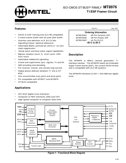
MT8976资料
19 28
DSTi
Data ST-BUS Input. This pin accepts a 2048 kbit/s serial stream which contains the 24 PCM or data channels to be transmitted on the T1 trunk.
2048-1544 Converter
DS1 Link Interface
Remote & Digital Loopbacks
ABCD Signalling RAM
Phase
DS1
Detector
Counter
•
Figure 1 - Functional Block Diagram
C1.5i RxFDLClk RxFDL RxA RxB TxA TxB TxFDLClk TxFDL RxD
TxA
Transmit A Output. Unipolar output that can be used in conjunction with TxB and
external line driver circuitry to generate the bipolar DS1 signal.
23
error count • Selectable robbed bit signalling • Frame and superframe sync. signals, Tx and Rx • AMI encoding and decoding • Per channel, overall, and remote loop around • Digital phase detector between T1 line & ST-
MP2315产品参数规格书

High Efficiency 3A, 24V, 500kHz Synchronous Step Down Converter
The Future of Analog IC Technology
DESCRIPTION
The MP2315 is a high frequency synchronous rectified step-down switch mode converter with built in internal power MOSFETs. It offers a very compact solution to achieve 3A continuous output current over a wide input supply range with excellent load and line regulation. The MP2315 has synchronous mode operation for higher efficiency over output current load range. Current mode operation provides fast transient response and eases loop stabilization. Full protection features include OCP and thermal shut down. The MP2315 requires a minimum number of readily available standard external components and is available in a space saving 8-pin TSOT23 package.
马扎克6800参数
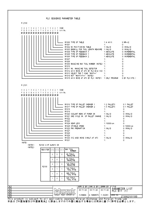
F E D C B A 9876543210bit No.0111120 TOOLS MAGAZINE 160 TOOLS TOOL HIVE bit 80101MAX TOOL NUMBER 40 TOOLS MAGAZINE 80 TOOLS MAGAZINE 240 TOOLS TOOL HIVE 320 TOOLS TOOL HIVEbit A REGISTER R2100<NOTE2><NOTE1> R2100 bitF ALWAYS ON <NOTE>M1029 1: 0:M1028 1: 0:M1027 1: 0:M1026 FMS PRERARTION 1:VALID 0:INVALID M1025 SPINDLE SPEED 1: 0:10000rpm M1024 GEAR LESS 1:10000rpm 0:M1023 1: 0:M1022 1: 0:0M1020 COOLANT MENU AT POWER ON 1:VALID 0:INVALID M1019 1: 0:M1018 1: 0:M1017 TYPE OF PALLET CHENGER 2 1:6 PALLETS 0:1 PALLET bit No.COAD M1021 ONE CYCLE SW. OF PALLET CHANGE 1:VALID 0:INVALID bit 9COAD 01M1016 TYPE OF PALLET CHENGER 1 1:2 PALLETS 0:1 PALLET M1015 AXIS MOVE AT ATC BY PLC <NOTE1> 1:ONLY PROGRAM 0:BY PLC(STD.)M1014 NOT "M06T**T**" <NOTE3> 1: 0:M1013 SELECT THE T COAD "M06T**" 1: 0:M1012 AXIS MOVE AT ATC BY PLC(EIA/ISO) 1: 0: M1011 NG. MAGAZINE TOOL DETECTOR 1: 0:M1009 MAGAZINE MAX TOOL NUMBER <NOTE2> 1: 0:M1007 1: 0: M1006 TYPE OF FEEDBACK Z 1:ABSOLUTE 0:INCREMENTAL M1005 TYPE OF FEEDBACK Y 1:ABSOLUTE 0:INCREMENTAL M1004 TYPE OF FEEDBACK X 1:ABSOLUTE 0:INCREMENTAL M1003 ENDMILL FOR TOOL LENGTH MEASURE 1:VALID 0:INVALIDM1002 NC POSITIONING TABLE 1:VALID 0:INVALID M1001 1: 0:1M1000 TYPE OF TABLE 1:4 AXIS 0:MR-J21248124812481248R 2100000F E D C B A 98765432101248124812481248R 2101PLC SEQUENCE PARAMETER TABLEM1031 1: 0:M1030 XYZ AXES MOVE SIMULT.AT ATC 1:VALID 0:INVALID M1008 1: 0: M1010 1: 0: APR'D BY 45TITLEDRWN BYCHK'D BYPARAMETER LIST PLC BIT (1)06/11/2006/11/2006/11/20M1062 TOOL ID 1:AVAILABLE 0:DISAVAILABLE M1055 USA-SUPER FLOW HIGH PRE.COOLANT 1:VALID 0:INVALID M1049 SPINDLE THROUGH COOLANT 1:VALID 0:INVALID M1045 1: 0:M1042 TOOL TRANSPORT SYSTEM 1:VALID 0:INVALID M1039 INCH/METRIC CONVERSION 1:VALID 0:INVALID M1035 RESERVED(MG) 1:VALID 0:INVALID M1063 1: 0:M1061 WAIT CUTTING FEED TILL COOLANT ON1:AVAILABLE 0:DISAVAILABLE M1058 SPIRAL CONVEYOR CMD BY M CODE 1:VALID 0:INVALID M1057 SPINDLE CLEANING TOOL 1:VALID 0:INVALID M1056 TOOL CLEANER 1:VALID 0:INVALID M1052 NATIONAL HIGH PRE.COOLANT 1:VALID 0:INVALID M1054 1:3(STD) 0:1(NEW)M1051 KNOLL HIGH PRE.COOLANT 1:VALID 0:INVALID M1050 OIL HOLE COOLANT 1:VALID 0:INVALID bit No.COAD M1053 NEW NATIONAL HIGH PRE.COOLANT 1:VALID 0:INVALID COAD M1048 CONSEP2000(MAYFRAN) 1:VALID 0:INVALID M1046 PATO LIGHT ON AT M00/M01 1:VALID 0:INVALID M1047 WARM UP ACTION 1:VALID 0:INVALIDM1043 MAZATROL-FMS 1:VALID 0:INVALID M1044 PALLET I/D 1:VALID 0:INVALID M1041 D.N.C 1:VALID 0:INVALID M1040 PATO LIGHT ON AFTER PALLET CHANGE1:VALID 0:INVALID M1038 CYCLE START BEFORE ZERO RETURN 1:VALID 0:INVALID M1037 1: 0:M1036 RESERVED(PD) 1:VALID 0:INVALID M1034 RESERVED(MD) 1:VALID 0:INVALID M1033 1: 0:M1032 MAZAK MESURING SYSTEM 1:VALID 0:INVALID 1248124812481248R 2102F E D C B A 98765431F E D C B A 987654321012481248124812480bit No.2R 2103M1059 TECNOFORME HIGH PRE. COOLANT I/F 1:VALID 0:INVALIDM1060 1:SP. STOP 0:SP. NOT STOP APR'D BY 45TITLEDRWN BYCHK'D BYPARAMETER LIST PLC BIT (2)06/11/2006/11/2006/11/20F E D C B A 9876543210bit No.RESERVED(YME-C) 1:VALID 0:INVALID HDLC MODE 1:TAPE 0:MEMORY M5031 P/C HOOK COMMAND ARBITARY POSITION 1:CMD.POSITION 0:CMD.OFFSETM5030 1:VALID 0:INVALID M5029 1:VALID 0:INVALID M5028 PMC (FLAT FMS) 1:VALID 0:INVALID M5027 1: 0:M5026M5024M5023 NEGLECT NEXT TOOL AT MMS OR TBR 1:VALID 0:INVALID M5022 1: 0:M5011 FHD AT THERMAL OFFSET ALARM 1:INVALID 0:VALIDM5004 1: 0:M5016 RESUME SPINDLE RUN AFTER ATC(EIA/ISO) 1:VALID 0:INVALID M5013 MMS INTERFACE UNIT TYPE 1:OMI 0:MI12M5010 HIGH SPEED SPINDLE WARM UP 1:AVAILABLE 0:DISAVAILABLE M5007 1: 0:M5003 1: 0:M5020 RESUME SPINDLE RUN AFTER ATC(MAZATROL) 1:VALID 0:INVALID M5017 WAIT CUTTING FEED TILL SP. UP TO SPEED 1:VALID 0:INVALIDM5019 1:VALID 0:INVALID M5018 NEGLECT NEXT TOOL 1:AVAILABLE 0:DISAVAILABLE bit No.COAD M5021 TOOL ID ALARM CANCEL 1:VALID 0:INVALID COAD M5015 TOUCH PROBE TYPE 1:MP10 0:MP3M5009 COLLECT SP. LOAD FOR WARM UP 1:INVALID 0:VALIDM5008 MMS SKIP BUZZER 1:INVALID 0:VALID M5005 1: 0:M5006 1: 0:M5002 1: 0: M5001 1: 0:M5000 1: 0:1248124812481248R 2104F E D C B A 98765432101248124812481248R 2105M5025 1: 0:M5012 TTS RUNNING (NEGLECT ID) 1:AVAILABLE 0:DISAVAILABLE M5014 STATES OF M/C WHEN MMS LOW BAT. 1:ALARM DSP.ONLY 0:FEED HOLD STOP APR'D BY 45TITLEDRWN BYCHK'D BYPARAMETER LIST PLC BIT (3)06/11/2006/11/2006/11/20WAIT ATC AT SP.THROU AIR 1:VALID 0:INVALID HYDRAULIC JIG TYPE B (2) 1:VALID 0:INVALID JET PURSUE 1:VALID 0:INVALID HYDRAULIC JIG TYPE A 1:VALID 0:INVALID #1033 RESET AT M02/M30 1:INVALID 0:VALID INCH/METRIC CONVERSION 1:VALID 0:INVALID PNo.-->#1033 (PALLET ID) 1:VALID 0:INVALID TABELE PALLET CHANGR POSSIOTION 1:180DEG(OP.) 0:0DEG NC POSITIONING TABLE COMMAND 1:1DEG=B1 0:1DEG=B1000 NEXT INSTRUCTION 1-CYCLE INVAL. 1:VALID 0:INVALID SPINDLE MONITOR(YME-C) 1:VALID 0:INVALID CHIP BLASTER/OGURA HIGH PRS.COOLANT 1:VALID 0:INVARID X&Y AXES MOVE WITH INDEX TABLE 1:VALID 0:INVALID OIL HOLE & SP.THROUGH COOLANT 1: 0:6PC No.CONF.SENSOR 1:VALID 0:INVALID THE SECOND COOLANT FILTER 1:VALID 0:INVALID M5062M5061M5060M5059M5058M5057M5056M5055M5054M5053M5052M5051 M5050M5049M5048M5047 ADDITIONAL M CODE 1:VALID 0:INVALIDM5038 WAY LUBE FLOWT SWITCH TYPE 1:LOW-ON 0:LOW-OFF M5037 THROUGH COOLANT INHIBIT AT SP ON 1:INVALID 0:VALID M5035 COIL CHANGE LOW BY ORIENT 1:INVALID 0:VALIDM5034 NEW PMC(MASTER MACHINE) 1:VALID 0:INVALID M5033M5032M5063 MR-J2 SET MENU 1:VALID 0:INVARIDbit No.COAD COAD 1248124812481248R 2106F E D C B A 98765431F E D C B A 987654321012481248124812480bit No.2R 2107PLC SEQUENCE PARAMETER TABLEM5039 OIL AIR FLOWT SWITCH TYPE 1:LOW-ON 0:LOW-OFF M5040 GEAR 4 1:VALID 0:INVALID M5041 OIL AIR PRESS SWITC TYPE 1:N.C. 0:N.O.M5042 LARGE DIA.BORING BAR 1:VALID 0:INVALID M5043 LUBERICATION PRESSURE SWITCH TYPE 1:N.C. 0:N.O.M5044 P/C HOOK CMD.ARBITARTY POSSITION 1:360 POS. 0:360000 POS.M5045 CYCLE FIN.BUZZER 1:VALID 0:INVALID M5046 PHS 1:VALID 0:INVALID PRESSURE SW. FOR THROUGH COOLANT 1:VALID 0:INVALID M5036 MACHINE ADJUSTMENT JIG 1:VALID 0:INVALID APR'D BY 45TITLEDRWN BYCHK'D BYPARAMETER LIST PLC BIT (4)06/11/2006/11/2006/11/20F E D C B A 9876543210bit No.M5079 CENTRALIZED COOLANT AND PALLET AIR BLAST 1:(Mercury) 0:INVALIDM5070 STOPS THE DOOR BY 6P/C DOOR OPENING 1:VALID 0:INVALID M5069 HANDLE BOX SP.JOG SW. 1:INVALID 0:VALID M5068 1: 0:M5092 HSK TOOL 1:VALID 0:INVALID M5091 1: 0: M5090 FMS DOOR ONE TOUCH OPEN 1:VALID 0:INVALID M5085 P/C START AT 1 CYCLE STOP 1:1 CYCLE SW. 0:1 CYCLE+CST SW.M5082 NC ROTARY TABLE SERVO OFF AT CLAMP 1:NOT SERVO OFF 0:SERVO OFF M5083 CHIP CONVEYER SLIP ALARM 1:VALID 0:INVALID M5078 1CYC.WILL NOT BE VALIDATE IF FIXTURE IS CLAMP 1:VALID 0:INVALID M5077 TOOL HIVE 1:VALID 0:INVALID M5076 COOLANT FILTER 1:VALID 0:INVALID M5075 WARM UP 1:VALID 0:INVALID M5074 1: 0:M5073 COOLANT STOP ALARM 1:VALID 0:INVALID M5072 1: 0:M5067 HYDRAULIC JIG TYPE B (1) 1:VALID 0:INVALID M5065 MMS ALARM 1:VALID 0:INVALID M5088 NEXT PALLET SELECT 1:VALID 0:INVALID M5094 HEIDENHAIN SCARE 1:VALID 0:INVALID M5089 1: 0:M5084 ALL AXIS ZERO RETURN AT WORM UP 1:INVALID 0:VALIDM5081 TOOL ID WRITABLE ONLY WHEN MAG.MNL.INTRR 1:VALID 0:INVALID bit No.COAD M5086 1: 0:COAD M5093 AUTO WARM UP 1:VALID 0:INVALID M5095 CYCLE START ACTIVET 1:ANY SCREEN 0:ONLY SPECM5080 TABLE AUTO ZERO RETURN AT PALLET CHANGE 1:INVALID 0:VALID M5066 COIL CHANGE MANUAL 1:VALID 0:INVALID 1248124812481248R 2108M5087 CUNV. ENABLE 1:INVALID 0:VALID F E D C B A 98765432101248124812481248R 2109M5064 PALLET SHELTER AFTER PALLET IS UNLOAD 1:VALID 0:INVALID M5071 1: 0:APR'D BY 45TITLEDRWN BYCHK'D BYPARAMETER LIST PLC BIT (5)06/11/2006/11/2006/11/20F E D C B A 9876543210bit No.bit No.COAD COAD M4058 1:VALID 0:INVALID 1248124812481248R 2143F E D C B A 98765432101248124812481248R 2144M4042 1:VALID 0:INVALID M4043 1:VALID 0:INVALID M4044 1:VALID 0:INVALID M4045 1:VALID 0:INVALID M4046 1:VALID 0:INVALID M4047 1:VALID 0:INVALID M4048 1:VALID 0:INVALID M4049 1:VALID 0:INVALID M4050 1:VALID 0:INVALID M4051 1:VALID 0:INVALID M4052 1:VALID 0:INVALID M4053 1:VALID 0:INVALID M4054 1:VALID 0:INVALID M4055 1:VALID 0:INVALID M4056 1:VALID 0:INVALID M4057 1:VALID 0:INVALIDM4059 1:VALID 0:INVALID M4060 1:VALID 0:INVALID M4061 1:VALID 0:INVALID M4062 1:VALID 0:INVALID M4063 1:VALID 0:INVALID M4064 1:VALID 0:INVALID M4065 1:VALID 0:INVALID M4066 1:VALID 0:INVALID M4067 1:VALID 0:INVALID M4068 1:VALID 0:INVALID M4069 1:VALID 0:INVALID M4070 1:VALID 0:INVALID M4071 1:VALID 0:INVALID M4072 1:VALID 0:INVALID M4073 1:VALID 0:INVALIDAPR'D BY 45TITLEDRWN BYCHK'D BYPARAMETER LIST PLC BIT (6)06/11/2006/11/2006/11/20F E D C B A 9876543210bit No.bit No.COAD COAD 1: 0:1248124812481248R 2148F E D C B A 98765432101248124812481248M4074 1:VALID 0:INVALID M4075 1:VALID 0:INVALID M4076 1:VALID 0:INVALID M4077 1:INVALID 0:VALID M4078 1:VALID 0:INVALID M4079 1:INVALID 0:VALID M4080 1:INVALID 0:VALID M4081 1: 0: 1: 0: 1: 0: 1: 0: 1: 0: 1: 0: 1: 0: 1: 0: 1: 0:1: 0: 1: 0: 1: 0: 1: 0: 1: 0: 1: 0: 1: 0: 1: 0: 1: 0: 1: 0: 1: 0: 1: 0: 1: 0: 1: 0: 1: 0:APR'D BY 45TITLEDRWN BYCHK'D BYPARAMETER LIST PLC BIT (7)06/11/2006/11/2006/11/20F E D C B A 9876543210bit No.COAD 1248124812481248R 22771:VALID 0:INVALID 1:MEMORY&MDI 0:MEMORY 1:RESET&1CYCLE0:1CYCLE SW.1:CLEAR&1CYCLE0:1CYCLE SW.1:VALID 0:INVALID 1:VALID 0:INVALID 1:HIGH/LOW 0:HIGH 1:VALID 0:INVALID 1:VALID 0:INVALID 1:VALID 0:INVALID 1:VALID 0:INVALID 1:VALID 0:INVALID 1:VALID 0:INVALID 1:VALID 0:INVALID 1:VALID 0:INVALIDPALLET CHANGE FIN.YELLOW PATO LIGHTPALLET CHANGE FIN.YELLOW PATO LIGHT ON 1PALLET CHANGE FIN.YELLOW PATO LIGHT ON 2PALLET CHANGE FIN.YELLOW PATO LIGHT OFF 1PALLET CHANGE FIN.YELLOW PATO LIGHT OFF 2PALLET CHANGE FIN.YELLOW PATO LIGHT REMEMBER(P.OFF)M4032M4033M4034M4035M4036M4037M4038M4039M4040M4041F E D C B A 9876543210bit No.COAD 12481248124812481: 0: 1: 0: 1: 0: 1: 0: 1: 0: 1: 0: 1: 0: 1: 0: 1: 0: 1: 0: 1: 0: 1: 0: 1: 0: 1: 0: 1: 0: 1: 0:1:MEMORY&MNL 0:MEMORYAPR'D BY 45TITLEDRWN BYCHK'D BYPARAMETER LIST PLC BIT (8)06/11/2006/11/2006/11/20F E D C B A 9876543210bit No.COAD 1248124812481248R 22801: 0:FOR OPTION 1: 0:FOR OPTION 1: 0:FOR OPTION 1: 0:FOR OPTION 1:VALID 0:INVALID1:VALID 0:INVALID JET GUN1:VALID 0:INVALID 2PC SAFETY DOOR1:VALID 0:INVALID RTN.PREVIOUS RAPID OVERRIDE WHEN MC DOOR CLOSE 1:VALID 0:INVALID EUCHNER TOOL ID 1:VALID 0:INVALID RESERVED (MDN)1:VALID 0:INVALID BALLUFF TOOL ID 1:NEAREST 0:CW1:NEAREST 0:COMMANDED 1:VALID 0:INVALID1:VALID 0:INVALID ADDITONAL AXIS 1:VALID 0:INVALIDD'ANDREA TOOL M4000M4001M4002M4003M4004M4005M4006M4007M4008M4009M4010M4011M4012M4013M4014M4015F E D C B A 9876543210bit No.COAD 1248124812481248R 22811:NO ALARM 0:MC STOP PROCESS FOR MC.OUTSIDE TBR.DET.M56,M55/EIA 1:VALID 0:INVALID OUTSIDE MACHINE TOOL BREAKAGE DETECTION 1:BUILT-IN 0:EUCHNER TOOL ID ID AMP.TYPE 1:VALID 0:INVALID1:VALID 0:INVALIDROBOT INTERFACE (USA-STD)1:AUTO 0:CYCLE START1:VALID 0:INVALID ROBOT INTERFACE(SILMECA/ACMS SPEC.)1:VALID 0:INVALID TROUGH COOLANT FLOOD/MIST SWITCH 1:VALID 0:INVALID EXTERNAL BLOCK SKIP1:BEFORE 0:ALL OFF SELECTION FOR BLOCK SKIP AT POWER ON 1:VALID 0:INVALID FLOOD COOLANT FLOW DETECTION 1:VALID 0:INVALID WARK GAP DETECTION 1:VALID 0:INVALID LONG TOOL INTERLOCK 1:VALID 0:INVALID HYDRAULIC FIXTURE A+B1:VALID 0:INVALID 1CYCLE SW. FOR BOTH HANDS(NEMAK)1:VALID 0:INVALIDPALLET DOOR AUTO OPEN AFTER PALLET CHANGE M4016M4017M4018M4019M4020M4021M4022M4023M4024M4025M4026M4027M4028M4029M4030M4031APR'D BY 45TITLEDRWN BYCHK'D BYPARAMETER LIST PLC BIT (9)06/11/2006/11/2006/11/20rpm ±%SPINDLE UP TO SPEED PERCENTAGErpm SPINDLE MOTOR COILING CHANGE SPEED HYSTERISYS LOW GEAR SPINDLE MOTOR COILING CHANGE SPEED LOW GEAR98 7 6 5 4 3 2 1R 2140 9 8 7 6 5 4 3 2 1PLC SW. & ALARM DISPLAY (LANGUAGE CODE)TOOL ID READ RETRY NUMBER (IF 0 THEN 3 TIMERS)TOOL ID MAGAZINE POCKET PARAMETERR 2130 9 8 7 6 5 4 3 2 1WARM UP WORK No.1~9999MULTIPLICATI0N OF M,P,G INTERRUPTION4 8 9rpmSPINDLE SPEED AT CLEANING TOOL ONR 2120SJOG VALLUE (SPINDLE JOG SPEED R,P,M) 6 5 3rpm 7%%R2 VALUE (RAPID TRAVERSE SPEED %)R 2130 0:ENG 1:JPNSPINDLE CLEANING TOOL No.% 2 2:*100 1:* 10R 2116 0:* 1<NOTE>R 2110 C O M M E N T ADDRESS R0 VALUE (RAPID TRAVERSE SPEED %)PLC DATA (SHORT TYPE) PARAMETERR1 VALUE (RAPID TRAVERSE SPEED %) 1 5 (NCTABLE:3)25 50 220500 52000 201510000rpmSPINDLE TYPESPINDLE SPEED AT JOGPALLET ID DELAY TIMER(PALLET ID OPTION ONLY)SCANSPINDLE LOAD LIMIT ALARM 1SPINDLE LOAD LIMIT ALARM 2SPINDLE LOAD CHANGE RATE 1SPINDLE LOAD CHANGE RATE 2SETTING UNIT3 (NCTABLE:2)PLC PARAMETERPLC PARAMETER PLC PARAMETERPLC PARAMETER APR'D BY 45TITLEDRWN BYCHK'D BYPARAMETER LIST PLC DATA (1)06/11/2006/11/2006/11/2050.01S MG.SHIFTER OFF TIMER3101800 6003002000150 10 5 18003600600700 150 D199D198D197D196D195D194D193D192D191D190D189D188D187D186D185D184D183D182D181D180D179D178D177D176D175D174D173D172D171D170 98 7 6 5 4 30.01S20.1S 10.1S OIL AIR TIMER 3(PUMP ON DELAY)R 2190 JE FILTER LEVEL LOW ALARM TIMER SPINDLE LOAD READING DELAY TIME AT SPINDLE CHANGE SPEED ALARM DISREGARD TIME AT AFTER SPINDLE CHANGE SPEED 0.1S 0.1SOIL AIR TIMER 2(UNIT OFF TIMER)OIL AIR TIMER 1(UNIT ON TIMER) 0.1℃0.1℃ SPINDLE OVER HEAT TEMPETURE SPINDLE OVER HEAT DIFFERENCE OF TEMPETURE SPINDLE START DIFFERENCE OF TEMPETURE PALLET AIR BLOW OFF TIMER PALLET AIR BLOW ON TIMER 0.1S 0.01S 0.01S times 0.01S 0.1S 0.1S 0.1S WARM UP WATING TIMERCOOLANT START TIMER WAY LUBE ALARM COUNTCYCLE FIN. BUZZER ON TIMER WAY LUBE OFF TIMERWAY LUBE ON TIMER AUTO POWER OFF DELAY 0.01S 8 9 7 6 5 4 3 2 1R 2180 9 8 7 6 5 4 3 2 1 R 2170 9 8 7 6 5 4 3 2 1 4 8 9R 2160 6 5 3 7 2R 2150 C O M M E N T400ADDRESS PLC DATA (SHORT TYPE) PARAMETER1TABLE UNCLAMP TIMER ATC TOOL CLAMP SENSOR DELAY TIMER SPINDLE TYPE10000rpmATC WAIT POKET SENSER DELAY TIMER HIGH PRESSURE COOLANT START TIMER OIL AIR ALARM COUNTER 100.01S 40.1S10.01SCYCLE FIN. BUZZER TIMER CYCLE FIN. BUZZER OFF TIMER PALLET CHANGE TIMER (FH8800)0.1S PALLET CHANGE HOOK UP TIMER 0.1S144020(NCTABLE:50)18002400APR'D BY 45TITLEDRWN BYCHK'D BYPARAMETER LISTPLC DATA (2)06/11/2006/11/2006/11/2098 7 6 5 4 3 2 1R 2190 9 8 7 6 5 4 3 2 1 4 8 9R 2280 6 5 3 7 2R 2270 C O M M E N TADDRESS PLC DATA (SHORT TYPE) PARAMETER1*1 2PC:0 6PC:6*2 2PC:0 6PC:3MAX PALLET NUMBER LOADING STATION POSITION*1*2BIT TYPEBIT TYPE BIT TYPE4 8 9 65 3 7 2R 2260 136064APR'D BY 45TITLEDRWN BYCHK'D BYPARAMETER LIST PLC DATA (3)06/11/2006/11/2006/11/200.1゜C OVER HEAT FOR 1 SAMPLING SCAN 0READ AND WRITE TIME OVER ALARM COUNTER DATA SCAN 0COUNTER DATA THAT MACHINE HAS TOOL ID OR NOT.(PLC-CMN PARAMETER LIST REFERENCE)00010-700 20080000.1゜CSCAN SCAN SCAN THRESOLDOFFSET VALVE BY ONE TIME FOR AFTER ATC OFFSET VALVE BY ONE TIMEOFFSET EXEC.DELAY COUNTER FOR AFTER ATC OFFSET EXEC.DELAY COUNTERRETRY COUNTER DATA OF RESPONSE SIGNAL RECEIVE bit TYPE8 8 7 7 6 6 5 5R 2844 4 3 2 1R 2340 9CLAMP SPEED AT GAP ELIMINATER ON1st OVERRAID AT GAP ELIMINATER SIGNAL OFF98 7 6 4 5 3 2 1 9 8 7 6 5 4 3 2 1 9 8 7 6 5 4 3 2 1MEMORY 9R 2330R 2320 4 8 9R 2310 6 5 3 7%mm/min2R 2300ADDRESS PLC PARAMETER (DATA TYPE)10.5μ0.5μ5835SCAN TOOL ID DELAY TIMER(TOOL ID OPTION ONLY)200APR'D BY 45TITLEDRWN BYCHK'D BYPARAMETER LIST PLC DATA (4)06/11/2006/11/2006/11/2012020 (8m/min) 11 40 10000 5000 5μmATC ARM EXTEND VALVE%%0.01%0.01%0.01%rpmrpmSPINDLE MAX. SPEED GEAR 1 AT VFC SPINDLE MAX. SPEED GEAR 2 AT VFC μmmm/minSEC TOOL LENGTH MEASURE RAPID TRAVERSE OVERRAID AFC UPPER THRESOLDAFC LOWER THRESOLD AFC STEP VALUE OF 2nd OVERRIDE Z AXIS SKIP POSITIONY AXIS START POSITION OF TOOL LENGTH MEASUREAFC MIN. VALUE OF 2nd OVERRIDE AFC ALARM TIME AFTER CLAMPPED 2nd 0V AFC MAX. VALUE OF 2nd OVERRIDE X AXIS START POSITION OF TOOL LENGTH MEASURETOOL LENGTH MEASURE SKIP SPEED8 8 7 7 6 6 5 5 4 4 3 3 2 2 1 1R 2890R 2390 9 9μm%μm98 7 6 4 5 3 2 1R 2880 9 8 7 6 5 4 3 2 1R 2870 9 8 7 6 5 4 3 2 1R 2860 9 8 7 6 5 4 2 3 1R 2850 2 1 9 8 7 6 5 4 3 2 1 9 8 7 6 5 4 3 2 1ACTIVE MEMORY 98 7 6 5 4 3R 2380R 2370 4 8 9R 2360 6 5 3 7DISTANCE OF THE TOW SENSOR SKIP AND DEC.Z AXIS START POSITION OF TOOL LENGTH MEASUREμmμm2R 2350 1105000(41338inch)27000(10630inch)APR'D BY 45TITLEDRWN BYCHK'D BYPARAMETER LIST PLC DATA (5)06/11/2006/11/2006/11/201126 -200 74 %%AFC UPPER THRESOLDAFC LOWER THRESOLD98 7 6 5 4 3 2 1R 9 8 7 6 5 4 3 2 1R 9 8 7 6 5 4 2 3 1R 98 7 6 5 4 3 2 1 9 8 7 6 5 4 3 2 1 3ACTIVE MEMORY R 4670 4 8 9R 4620 6 5 7 2R 3980 120000(7874inchi)APR'D BY 45TITLEDRWN BYCHK'D BYPARAMETER LIST PLC DATA (6)06/11/2006/11/2006/11/20TOOL ID 1:VALID 0:INVALID FMC CONTROL ID 1:VALID 0:INVALID MANUAL MEASURE 1:VALID 0:INVALID F E D C B A 987DATA AT MANUAL WRITE 1:ONLY FLAG 0:ALL DATA TOOL ID R RESISTOR LOADE 1:VALID 0:INVALID THERMAL DISPLACEMENT MACRO VARIABLE WRITE 1:VALID 0:IVVALID V100 ONLY 1:VALID 0:INVALID V100 ONLY 1:VALID 0:INVALID V100 ONLY 1:VALID 0:INVALID TOOL ID SERIAL TYPE 1:VALID 0:INVALID TOOL INTERFERENCE MAX FRM 1:VALID 0:INVALIDFMC CONTROL 1:VALID 0:INVALID TOOL ID SERIAL TYPE 1:VALID 0:INVALID TOOL LENGTH TO LIFE INDEX DISPLAY AT READ 1:OFF SET NO. 0:COMPENSATION 4READ AND WRITE TO LIFE CONTROL DISPLAY 1:VALID 0:INVALID ID NO. AT WRITE 1:VALID 0:INVALID LIFE AT WRITE 1:LIFE CONTROL 0:TOOL DATA TOOL LENGTH TO LIFE INDEX DISPLAY AT READ 1:VALID 0:INVALID6521013bit No.COAD THERMAL DISPLACEMENT OFF SET 1:VALID 0:INVALID TOOL DIAMETER READ AND WRITE TOOL COM. TYPE A 1:VALID 0:INVALIDPROTECT SPINDLE TOOL AND NEXT TOOL NO. OF WRITE1:VALID 0:IVVALID FLAG AT WRITE 1:LIFE OR TOOL 0:TOOL DATA FLAG TO LIFE INDEX DISPLAY AT READ 1:VALID 0:INVALID READ AND WRITE TO ID NO. GROUP NO. 1:VALID 0:INVALID TOOL DIAMETER AT WRITE 1:LIFE CONTROL 0:TOOL DATA TIME TO LIFE INDEX DISPLAY AT READ 1:VALID 0:INVALID TOOL LENGTH AT WRITE 1:LIFE CONTROL 0:TOOL DATA TOOL LENGTH TO LIFE INDEX DISPLAY AT READ 1:OFF SET NO. 0:COMPENSATION TOOL LENGTH TO LIFE INDEX DISPLAY AT READ 1:VALID 0:INVALIDF E D C B A 98765432101248124812481248R 2301FMS PALLET ID 1:VALID 0:INVALID VARIABLE TIMER 1:VALID 0:INVALID COAD bit No.V100 ONLY 1:VALID 0:INVALID 248124812481248R 2300APR'D BY 45TITLEDRWN BYCHK'D BYPLC-CMNPARAMETER LIST (1)06/11/2006/11/2006/11/20MEASUREMENT DATA AT WRITE 1:VALID 0:INVALID PALLET NO. DISPLAY TO MACHINING CONTROL DISPLAY 1:VALID 0:INVALID FIXTURE OFF SET AT WRITE 1:VALID 0:INVALID F E D C B A 987H-400N HEAD 1ch TYPE 1:VALID 0:INVALID 1: 0:MACHINING UN FINISH / NACHINING FLAG AT WRITE 1:VALID 0:INVALID ARBITRARY 1 BYTE WRITE AT WRITE 1:HEAD No.1 0:HEAD No.2COMMUNICATION PARAMETER MANUAL INPUT 1:VALID 0:INVALID PROGRAM DISPLAY TO MACHINING CONTROL DISPLAY 1:VALID 0:INVALIDNOTE 1: 1: 0:COMMUNICATION PARAMETER MANUAL INPUT 1:VALID 0:INVALID 46521013bit No.COAD 1: 0:USR 1 DISPLAY COMPULSION PARAMETER 1:VALID 0:INVALID USR 1 PARAMETER 1:VALID 0:INVALID F E D C B A 98765432101248124812481248R 2303NOTE 1: 1: 0:BASIC COORDINATE AT WRITE 1:VALID 0:INVALID COAD bit No.ARBITRARY 1 BYTE WRITE AT WRITE 1:VALID 0:INVALID248124812481248R 2302USR 2 PARAMETER 1:VALID 0:INVALID USR 3 PARAMETER 1:VALID 0:INVALID USR 4 PARAMETER 1:VALID 0:INVALID USR 5 PARAMETER 1:VALID 0:INVALID USR 6 PARAMETER 1:VALID 0:INVALID USR 7 PARAMETER 1:VALID 0:INVALID USR 8 PARAMETER 1:VALID 0:INVALID USR 2 DISPLAY COMPULSION PARAMETER 1:VALID 0:INVALID USR 3 DISPLAY COMPULSION PARAMETER 1:VALID 0:INVALID USR 4 DISPLAY COMPULSION PARAMETER 1:VALID 0:INVALID USR 5 DISPLAY COMPULSION PARAMETER 1:VALID 0:INVALID USR 6 DISPLAY COMPULSION PARAMETER 1:VALID 0:INVALID USR 7 DISPLAY COMPULSION PARAMETER 1:VALID 0:INVALID USR 8 DISPLAY COMPULSION PARAMETER 1:VALID 0:INVALIDbit 7bit 6COMMON VARIABLE001010#530~#549#580~#599#680~#699NOTE 1:APR'D BY 45TITLEDRWN BYCHK'D BYPLC-CMNPARAMETER LIST (2)06/11/2006/11/2006/11/20TOOL USE WRONG FLAG 1:VALID 0:INVALID F E D C B A 987NEXT PALLET NO. OUTPUT 1:VALID 0:INVALID 4DC BATTERY LIFE CHECK 1:VALID 0:INVALID 6521013bit No.COAD NUMBER OF TIME 1:ADD 0:SUBTRACT AFTER MACHINING FINISH LAST PLAN AUTO ALLOTMENT1:STAND 0:MEANLOADING STATION FINISH OPERATION 1:OK 0:STAND F E D C B A 98765432101248124812481248R 2305TOOL DATA ID NO. DISPLAY 1:HEXA DECIMAL 0:DECIMAL COAD bit No.248124812481248R 23041: 0:1: 0: 1: 0: 1: 0: 1: 0: 1: 0: 1: 0: 1: 0: 1: 0: 1: 0: 1: 0: 1: 0: 1: 0: 1: 0:1: 0: 1: 0: 1: 0: 1: 0: 1: 0: 1: 0: 1: 0: 1: 0: 1: 0: 1: 0: 1: 0:APR'D BY 45TITLEDRWN BYCHK'D BYPLC-CMNPARAMETER LIST (3)06/11/2006/11/2006/11/20NOTE 1 : 10111 FH680F E D C B A 987V40 TOOL LENGTH TYPE CHANGED INPUT DUMMY AT EXTENSION ONESELF DIAG. 46521013USR 3 MENU KEY NOTE 1 :THERMAL DISPLACEMENT MACHINE TYPECOAD bit No.248124812481248R 23091: 0:1: 0:1: 0:1: 0:1: 0:1: 0:1: 0:1: 0:1: 0:1: 0:1: 0:1:VALID 0:INVALID 1:VALID 0:INVALID1: 0:1: 0:1:VALID 0:INVALIDAPR'D BY 45TITLEDRWN BYCHK'D BYPLC-CMNPARAMETER LIST (4)06/11/2006/11/2006/11/20。
ansys软件问答合集(二)
47 在Ansys中,碰到提示“Volume 1 cannot be meshed. 208 location(s) found where non-adjacent boundary triangles touch. Geometry configuration may not be valid or smaller element size definition may be required.”。这是什么问题? 回答:提示就是告诉你需要更小的单元,可能单元太大的时候出现的网格有有问题,比如狭长 的网格,计算的时候集中应力太大。
48 在Ansys中,碰到错误Volume11 could not be swept because a source and a target area could not be determined automatically。please try again...,这是什么原因? 回答:体不符合SWEEP的条件,把体修改成比较规则的形状,可以分割试试。 49 在Ansys中,碰到警告和错误:“*** WARNING *** SUPPRESSED MESSAGE CP = 1312.641 TIME= 16:51:48 An error has occurred writing to the file = 12 which may imply a full disk. The system I/O error = 28. Please refer to your system documentation on I/O errors. ”,这是什 么错误和警告? 回答:1.I/O设备口错误,I/O=26,错误,告诉你磁盘已满,让你清理磁盘。但是实际问题的解 决不是这样,是你的磁盘格式不对,将你的磁盘格式从FAT26改称NTFS的就可以了。因为 FAT26格式的要求你的单一文件不能大于4G。但是我们一旦做瞬态或者是谐相应的时候都很 容易超过这个数,所以系统抱错。Байду номын сангаас2.I/O设备口错误,I/O=9,错误,和上一个一样告诉你磁盘已满,让你清理磁盘。但是实际问题 是由于你的磁盘太碎了造成的,你只要进行磁盘碎片整理就可以了,这个问题就迎刃而解。
ET(歌词)
Y ou're so hypnotizing你令人神魂颠倒Could you be the devil, could you be an angel.你可能变成魔鬼,你可以变成天使Y our touch magnetizing你的触摸很有磁性Feels like going floating, leave my body glowing就像在漂流,我的身体通红They say be afraid他们说害怕你Y ou're not like the others, futuristic lovers你和别人不一样,我的未来情人Different DNA, they don't understand U 不一样的基因,他们都不懂你Y ou're from a whole other world你来自一个完全不同的世界A different dimension不同的维度Y ou open my eyes你让我大开眼界And I'm ready to go我准备走了Lead me into the light把我带进光里吧Kiss me, ki-ki-kiss me吻我,吻-吻-吻我Infect me with your love and fill me with your poison用你的爱注射我用你的毒填满我Take me, ta-ta-take me带上我,带-带-带上我Wanna be your victim我可以被你杀死Ready for abduction准备好被你诱惑Boy, you're an alienBoy,你就是个外星人Y our touch so foreign你的触摸很陌生It's supernatural它是神奇的Extraterrestrial来自外星的Y ou are so supersonic你是超声波的Wanna feel your powers想感受你的力量Stun me with your lasers用你的激光吓我Y our kiss is cosmic你的吻是宇宙的Every move is magic每个动作都是神奇的Y ou're from a whole other world 你来自一个完全不同的世界A different dimension不同的维度Y ou open my eyes你让我大开眼界And I'm ready to go我准备走了Lead me into the light把我带进光里吧Kiss me, ki-ki-kiss me吻我,吻-吻-吻我Infect me with your love and fill me with your poison用你的爱注射我用你的毒填满我Take me, ta-ta-take me带上我,带-带-带上我Wanna be your victim我愿意做你的牺牲品Ready for abduction准备好被你诱惑Boy, you're an alienBoy,你就是个外星人Y our touch so foreign你的触摸很陌生It's supernatural它是神奇的Extraterrestrial来自外星的There is transcendental这是超乎经验的On another level在另一个层面上Boy, you're my lucky star男孩,你是我的幸运星I wanna walk on your wave length我想要与你合拍And be there when you vibrate当你摇摆不定的时候我会在那儿For you I risk it all为你我不惧怕任何危险Kiss me, ki-ki-kiss me吻我,吻-吻-吻我Infect me with your love and fill me with your poison用你的爱注射我用你的毒填满我Take me, ta-ta-take me带上我,带-带-带上我Wanna be your victim我愿意做你的牺牲品Ready for abduction准备好被你诱惑Boy, you're an alienBoy,你就是个外星人Y our touch so foreign 你的触摸很陌生It's supernatural它是神奇的Extraterrestrial来自外星的Extraterrestrial来自外星的Extraterrestrial来自外星的Boy, you're an alien Boy,你就是个外星人Y our touch so foreign 你的触摸很陌生It's supernatural它是神奇的Extraterrestrial来自外星的。
MT90863AL1资料
1Features•2,048× 512 and 512 x 512 switching among backplane and local streams•Rate conversion between 2.048, 4.096 and 8.192Mb/s•Optioal sub-rate switch configuration for 2.048 Mb/s streams•Per-channel variable or constant throughput delay•Compatible to HMVIP and H.100 specifications •Automatic frame offset delay measurement •Per-stream frame delay offset programming •Per-channel message mode •Per-channel direction control•Per-channel high impedance output control •Non-multiplexed microprocessor interface •Connection memory block programming • 3.3V local I/O with 5V tolerant inputs and TTL-compatible outputs•IEEE-1149.1 (JTAG) Test PortApplications•Medium and large switching platforms •CTI application•Voice/data multiplexer•Support ST-BUS, HMVIP and H.100 interfacesDescriptionThe MT90863 Rate Conversion Switch provides switching capacities of 2,048× 512 channels between backplane and local streams, and 512 x 512 channels for local streams. The connected serial inputs and outputs may have 32, 64 and 128 64kb/s channels per frame with data rates of 2.048Mb/s,4.096Mb/s and 8.192Mb/s respectively.The MT90863 also offers a sub-rate switching configuration which allows 2-bit wide 16kb/s data channels to be switched within the device.The device has features (such as: message mode;input and output offset delay; direction control; and,high impedance output control) that are programmable on per-stream or per-channel basis.Figure 1 - Functional Block DiagramF0o DS CS R/W A7-A0DTA D15-D0C16i Test PortOutput MuxMicroprocessor InterfaceTiming UnitInternal Backplane Connection Data Memory ODEV SSV DD TDI TDO RESET TCK TRSTTMS Interface Backplane ConverterP/S &S/P F0i C4i/C8iC4o STo0STo11STo12STo13STo15STi0STi11STi12STi13STi15(2,048 channels)(2,048 locations)Local Memory High/Low (512 locations)Multiple Buffer Data Memory (512 channels)Multiple Buffer Data Memory (512 channels)RegistersIC1ODEP/S ConverterLocal Interface S/P ConverterLocal InterfaceSTio0/STio15/FEi15FEi0STio16/STio23/FEi23FEi16STio24STio31IC2Connection Memory Multiple Buffer Ordering InformationMT90863AL1128 Pin MQFP MT90863AG1144 Pin BGA-40 to +85 CDS5034ISSUE 3March 1999MT908633V Rate Conversion Digital SwitchAdvance Information元器件交易网MT90863Advance Information2Figure 2 - MQFP Pin Connections128 Pin PQFP79858789717375779367916965838195111117119121103105107109125991231019711511312749474543415759555351393735616333171197252321193295273113151D14D12D11D10D9D8D6D5D4D3D2DTAD13D15STi13STi12STi11STi10STi9STi8STi7STi6STi4STi3STi2STi1STi0STi5VDDVSSVSSD7VDDSToSTo1STo2STo3STo4STo5STo6STo7VSSVDDODESTo8STo9STo1STo11STo12STo13STo14ST15VSSVSSFiFoC4oVSSC16iVSSVSSSTi14STi15STio0/FEi0STio1/FEi1STio2/FEi2STio3/FEi3STio4/FEi4STio5/FEi5STio6/FEi6STio7/FEi7STio8/FEi8STio9/FEi9STio11/FEi11STio15/FEi15STio10/FEi10STio12/FEi12STio13/FEi13STio14/FEi14STio16/FEi16STio17/FEi17STio18/FEi18STio19/FEi19STio20/FEi20VSSVDDSTio21/FEi21STio22/FEi22STio23/FEi23STio24VDDVSSVDDVSSVDDR/WTCKTDOA6A5A4A3A2A1ADSA7TDID1DVDDTRSTIC1TMSRESETVSSSTio25STio26STio27STio28STio29STio3STio31VSSVSSCSIC2C4i/C8i元器件交易网Advance InformationMT908633Figure 3 - BGA Pin ConnectionsPin Description128 MQFP Pin#144 BGA Pin#Name Description30,50,67,79,97,107,117,127C5,C9,D5,D7,D9,E10,F4,G10,G11,H4,K3,K4,K6,K8K10,K11,L8V DD+3.3 Volt Power Supply8,17,29,39,49,68,78,88,90,93,96, 106,116,126C6,C10,D4,D6,D8,D10,E3,E4,F10,F11,G2,G4,H10,J4,J10,J11,K5K7,K9,L3,L7V ssGround89D12C16i Master Clock (5V Tolerant Input):Serial clock for shifting data in/out on the serial streams. This pin accepts a 16.384 MHz clock.91D11F0iMaster Frame Pulse (5V Tolerant Input): In ST -BUS mode, this input accepts a 61ns wide negative frame pulse. In CT Bus mode, it accepts a 122ns wide negative frame pulse. In HMVIP mode, it accepts a 244ns wide negative frame pulse.1 - A1 corner is identified by metallized markings.BCDEFGHJKLMN12345678910111213TOP VIEW1A STio25STio26STio27STio28STio29STio30STio31TMS TDI TDOTCKTRSTIC1RESET A0A1A2A3A4A5A6A7DSR/WCSD0D1D2D3D4D5D6D7D8D9D10D11D12D14D13D15DT ASTi0STi1STi2STi3STi4STi5STi6STi7STi8STi9STi10STi11STi12STi13STi14STi15ODESTo0STo1STo2STo3STo4STo5STo6STo7STo8STo9STo10ST o11STo12ST o13ST o14ST o15C16i F0iC4i/C8i C4o F0oSTio0STio1STio2STio3STio4STio5STio6STio7STio8STio9STio10STio11STio12STio13STio14STio15STio16STio17STio18STio19STio20STio21STio22STio23STio24VSSVSSVSSVSSVSS VSS VSS VDDVDDVDDVDDVDDVDDVSSIC2VDDVSSVDDVSSVDDVSSVSSVSSVDDVSSVDDVSSVDDVDDVSSVDD VSSVSSVDDVDDVSSVSSVDDVSS元器件交易网MT90863Advance Information492B13C4i/C8i HMVIP/CT Bus Clock (5V Tolerant Input):When HMVIP mode isenabled, this pin accepts a 4.096MHz clock for HMVIP frame pulsealignment. When CT Bus mode is enabled, it accepts a 8.192MHzclock for CT frame pulse alignment.94A13F0o Frame Pulse (5V Tolerant Output): A 244ns wide negative framepulse that is phase locked to the master frame pulse (F0i).95C12C4o C4 Clock (5V Tolerant Output):A 4.096MHz clock that is phaselocked to the master clock (C16i).98-105,108-115C11, B12, B11,A12, A11, B10,A10, B9, A9,C8, B8, A8, C7,B7, A7, A6,STio0 - 15FEi0 - 15Serial Input Streams 0 to 15 / Frame Evaluation Inputs 0 to 15 (5VTolerant I/O). In 2Mb/s and HMVIP modes, these pins accept serialTDM data streams at 2.048 Mb/s with 32 channels per stream. In 4Mb/s or 8Mb/s mode, these pins accept serial TDM data streams at 4.096or 8.192 Mb/s with 64 or 128 channels per stream respectively. InFrame Evaluation Mode (FEM), they are frame evaluation inputs.118-125B6, A5, B5, A4,B4, C4, A3, B3STio16 - 23FEi16 - 23Serial Input Streams 16 to 23 (5V Tolerant I/O). In 2Mb/s or 4Mb/smode, these pins accept serial TDM data streams at 2.048 or 4.096Mb/s with 32 or 64 channels per stream respectively. In HMVIP mode,these pins have a data rate of 8.192Mb/s with 128 channels perstream. In Frame Evaluation Mode (FEM), they are frame evaluationinputs.128,1-7A2, B2, A1, C3,C2, B1, D3, D2STio24 - 31Serial Input Streams 24 to 31 (5V Tolerant I/O). These pins are onlyused for 2Mb/s or 4Mb/s mode. They accept serial TDM data streamsat 2.048 or 4.096 Mb/s with 32 or 64 channels per stream respectively.9C1TMS Test Mode Select (3.3V Input with internal pull-up):JTAG signalthat controls the state transitions of the TAP controller.10D1TDI Test Serial Data In (3.3V Input with internal pull-up):JTAG serialtest instructions and data are shifted in on this pin.11E2TDO Test Serial Data Out (3.3V Output):JTAG serial data is output on thispin on the falling edge of TCK. This pin is held in a high impedancestate when JT AG scan is not enabled.12E1TCK Test Clock (5V Tolerant Input):Provides the clock to the JTAG testlogic.13F2TRST Test Reset (3.3 V Input with internal pull-up):Asynchronouslyinitializes the JTAG T AP controller by putting it in the T est-Logic-Resetstate. This pin should be pulsed low on power-up, or held lowcontinuously, to ensure that the MT90863 is in the normal operationmode.14F3IC1Internal Connection 1 (3.3V Input with internal pull-down):Connect to V SS for normal operation.15F1RESET Device Reset (5V Tolerant Input): This input (active LOW) puts theMT90863 in its reset state. This clears the device’s internal countersand registers. It also brings microport data bus STio0 - 31 and STo0 -15 to a high impedance state.16G3IC2Internal Connection 2 (3.3V Input):Connect to V SS for normal operation.Pin Description (continued)128 MQFPPin#144 BGAPin#Name Description元器件交易网Advance InformationMT90863518-25G1, H1, H2,H3, J2, J1,J3,K1A0 - A7Address 0 - 7 (5V Tolerant Input): These lines provide the A0 to A7address lines to the internal memories.26K2DS Data Strobe (5V Tolerant Input): This active low input works in conjunction with CS to enable the read and write operations.27L2R/W Read/Write (5V Tolerant Input): This input controls the direction of the data bus lines (D0-D15) during a microprocessor access.28L1CS Chip Select (5V Tolerant Input):Active low input used by a microprocessor to activate the microprocessor port.31-38,40-47M1, N1, M2, N2,M3, L4, N3, L5,M4, N4, M5,L6, M6, N5, N6,M7,D0 - 7,D8 - D15Data Bus 0 -15 (5V Tolerant I/O): These pins form the 16-bit data bus of the microprocessor port.48N7DT AData Transfer Acknowledgment (5V Tolerant Three-state Output):This active low output indicates that a data bus transfer is complete. A pull-up resistor is required to hold a HIGH level when the pin is tri-stated.51-54N8, M8, N9,N10STi0 - 3Serial Input Streams 0 to 3 (5V Tolerant Inputs): In 2Mb/s orSubrate Switching mode, these inputs accept data rates of 2.048 Mb/s with 32 channels per stream. In 8Mb/s mode, these inputs accept data rates of 8.192 Mb/s with 128 channels per stream.55-62M9, N11, L9,M10, L10, N12,M11, N13STi4 - 11Serial Input Streams 4 to 11 (5V Tolerant Inputs): In 2Mb/s or Sub-rate Switching mode, these inputs accept data rates of 2.048Mb/s with 32 channels per stream.63L11STi12Serial Input Streams 12 (5V Tolerant Input): In 2Mb/s mode, this input accepts data rate of 2.048Mb/s with 32 channels per stream respectively. In Sub-rate Switching mode, this pin accepts 2.048Mb/s with 128 channels per stream for Sub-rate switching application.64-66M12, M13, L12STi13 - 15Serial Input Streams 13 to 15 (5V Tolerant Inputs): In 2Mb/s mode,these inputs accept a data rate of 2.048Mb/s with 32 channels per stream.69L13ODEOutput Drive Enable (5V Tolerant Input):This is the output enable control for the STo0 to STo15 serial outputs and STio0 to STio31 serial bidirectional outputs.70-73K13, K12, J13,J12ST o0 - 3Serial Output Streams 0 to 3 (5V Tolerant Three-state Outputs): In 2Mb/s or Sub-rate Switching mode, these outputs have data rates of 2.048 Mb/s with 32 channels per stream respectively. In 8Mb/s mode,these outputs have data rates of 8.192 Mb/s with 128 channels per stream74-77,80-83H11, H13, H12,G13, G12, F13,F12, E13ST o4 - 7,ST o8 - 11Serial Output Streams 4 to 11 (5V Tolerant Three-state Outputs):In 2Mb/s or Sub-rate Switching mode, these outputs have data rates of2.048Mb/s with 32 channels per streamPin Description (continued)128 MQFP Pin#144 BGA Pin#Name Description元器件交易网MT90863Advance Information6Device OverviewThe Rate conversion Switch (MT90863) can switch up to 2,048× 512 channels while also providing a rate conversion capability. It is designed to switch 64kb/s PCM or N X 64 kb/s data between the backplane and local interfaces. When the device is in the sub-rate switching mode, 2-bit wide 16 kb/s data channels can be switched within the device. The device maintains frame integrity in data applications and minimum throughput delay for voice application on a per channel basis.The backplane interface can operate at 2.048, 4.096or 8.192 Mb/s, arranged in 125µs wide frames that contain 32, 64 or 128 channels, respectively. A built-in rate conversion circuit allows users to interface between backplane interface and the local interface which operates at 2.048 Mb/s or 8.192 Mb/s.By using Mitel’s message mode capability, the microprocessor can access input and output time-slots on a per channel basis. This feature is useful for transferring control and status information for external circuits or other ST -Bus devices.The frame offset calibration function allows users to measure the frame offset delay for streams STio0 to STio23. The offset calibration is activated by a frame evaluation bit in the frame evaluation register. The evaluation result is stored in the frame evaluation registers and can be used to programme the input offset delay for individual streams using internal frame input offset registers.Functional DescriptionA functional Block Diagram of the MT90863 is shown in Figure 1. One end of the MT90863 is used to interface with backplane applications, such as HMVIP or H.100 environments, while the other end supports the local switching environments.Frame Alignment TimingThe Device Mode Selection (DMS) register allows users to select three different frame alignment timing modes. In ST -BUS modes, the master clock (C16i) is always at 16.384 MHz. The frame pulse (F0i) input accepts a negative frame pulse at 8kHz. The frame pulse goes low at the frame boundary for 61ns. The frame pulse output F0o provides a 244ns wide negative frame pulse and the C4o output provides a 4.094MHz clock. These two signals are used to support local switching applications. See Figure 4 for the ST -BUS timings.In CT Bus mode, the C4i/C8i pin accepts 8.192MHz clock for the CT Bus frame pulse alignment. The F0i is the CT bus frame pulse input. The CT frame pulse goes low at the frame boundary for 122ns. See Figure 5 for the CT Bus timing.In HMVIP mode, the C4i/C8i pin accepts 4.096MHz clock for the HMVIP frame pulse alignment. The F0i is the HMVIP frame pulse input. The HMVIP frame pulse goes low at the frame boundary for 244ns. See Figure 6 for the HMVIP timing.Table 1 describes the input timing requirements for ST -BUS, CT Bus and HMVIP modes.Switching ConfigurationThe device has four operation modes for the backplane interface and three operation modes for the local interface. These modes can be programmed via the Device Mode Selection (DMS)register. Mode selections between the backplane and local interfaces are independent. See Table 2and Table 3 for the selection of various operation modes via the programming of the DMS register.84E12ST o12Serial Output Streams 12 (5V Tolerant Three-state Output): In 2Mb/s mode, this output has data rate of 2.048Mb/s with 32 channels per stream. In Sub-rate Switching mode, this pin has data rate of 2.048Mb/s with 128 channels per stream for Sub-rate switching application.85-87D13, E11, C13ST o13 - 15Serial Output Streams 13 to 15 (5V Tolerant Three-state Outputs):In 2Mb/s mode, these outputs have a data rate of 2.048Mb/s with 32channels per stream.Pin Description (continued)128 MQFP Pin#144 BGA Pin#Name Description元器件交易网Advance InformationMT908637Figure 4 - ST-BUS Timing for 2, 4 and 8 Mb/s Data StreamsFigure 5 - CT Bus Mode Timing for 2, 4 and 8 Mb/s Data StreamsF0iC16i 7234561STio 0 - 15STi/STo 0 - 15(8Mb/s mode)12345617Channel 127Channel 07671Channel 31Channel 0(2Mb/s mode)F0oC4o1STi12/STo12(Sub-rate Bit 11Channel 127Channel 0Switching)STi/STo 0 - 375640STio 0 - 31(4Mb/s mode)1237Channel 63Channel 0STio 0 - 31F0iC4i/C8i F0oC4oC16i(8.192MHz) (CT_FRAME)7234561STio 0 - 15STi/STo 0 - 15(8Mb/s mode)12345617Channel 127Channel 07671Channel 31Channel 0(2Mb/s mode)01STi12/STo12(Sub-rate Bit 11Channel 127Channel 0Switching)STi/STo 0 - 37564STio 0 - 31(4Mb/s mode)1237Channel 63Channel 0STio 0 - 31元器件交易网MT90863Advance Information8Figure 6- HMVIP Mode Timing for 2 and 8 Mb/s Data StreamsF0iC4i/C8i72345610STio 16 - 23(8Mb/s mode)123456107Channel 127Channel 0F0oC4o010STi12/STo12(Sub-rate Bit 11Channel 127Channel 0C16iSwitching)(HMVIP Frame)(4.096MHz)07671Channel 31Channel 0STi/STo 0 - 15(2Mb/s mode)STio 0 - 15Backplane InterfaceThe backplane interface can be programmed to accept data streams of 2Mb/s, 4Mb/s or 8Mb/s. When 2Mb/s mode is enabled, STio0 to STio31 have a data rate of 2.048Mb/s. When 4Mb/s mode is enabled, STio0 to STio31 have a data rate of 4.096Mb/s. When 8Mb/s mode is enabled, STio0 to STio15 have a data rate of 8.192Mb/s. When HMVIP mode is enabled, STio0 to STio15 have a data rate of 2.048Mb/s and STio16 to STio23 have a data rate of 8.192Mb/s.Table 2 describes the data rates and mode selection for the backplane interface.Local InterfaceThree operation modes, 2Mb/s, 8Mb/s and Sub-rate Switching mode, can be selected for the local interface. When 2Mb/s mode is selected, STi0 to STi15 and STo0 to STo15 have a 2.048Mb/s data rate. When 8Mb/s mode is selected, STi0 to STi3 and STo0 to STo3 have an 8.192Mb/s data rate. When Sub-rate Switching mode is selected, STi0 to STi11 and STo0 to STo11 have 2.048Mb/s data with 64kb/s data channels and STi12 and STo12 have a 2.048Mb/s data rate with 16kb/s data channels. Table 3 describes the data rates and mode selection for the local interface.Input Frame Offset SelectionInput frame offset selection allows the channel alignment of individual backplane input streams, that operate at 8.192Mb/s (STio0-23), to be shifted against the input frame pulse (F0i). This feature compensates for the variable path delays caused by serial backplanes of variable length. Such delays can be occur in large centralized and distributed switching systems.Each backplane input stream can have its own delay offset value by programming the input delay offset registers (DOS0 to DOS5). Possible adjustment can range up to +4 master clock (C16i) periods forward with resolution of half master clock period. See Table 10 and Table 11, and Figure 9, for frame input delay offset programming.Output Advance Offset SelectionThe MT90863 allows users to advance individual backplane output streams which operate at 8.192Mb/ s (STio0-23) by half a master clock (C16i) cycle. This feature is useful in compensating for variable output delays caused by various output loading conditions. The frame output offset registers (FOR0 & FOR1) control the output offset delays for each backplane output stream via the OFn bit programming. Table 12 and Figure 10 detail frame output offset programming.Serial Input Frame Alignment EvaluationThe MT90863 provides the frame evaluation inputs, FEi0 to FEi23, to determine different data input delays with respect to the frame pulse F0i. By using the frame evaluation input select bits (FE0 to FE4) of元器件交易网Advance InformationMT908639Timing Signals ST -BUS ModeCT Bus ModeHMVIP ModeF0i Width 61ns 122ns 244ns C4i/C8i Not Required8.192MHz 4.096MHzC16i 16.384MHz F0o Width 244ns C4o4.096MHzTable 1 - Timing Signals Requirements for Various Operation ModesDMS Register BitsModesBackplane InterfaceData RateBMS2BMS1BMS00002Mb/s, ST -BUS Mode STio0 - 31 2.048 Mb/s 0012Mb/s, CT Bus Mode STio0 - 31 2.048 Mb/s 0104Mb/s, ST -BUS Mode STio0 - 31 4.096 Mb/s 0114Mb/s, CT Bus Mode STio0 - 31 4.096 Mb/s 18Mb/s, ST -BUS ModeSTio0 - 158.192 Mb/s STio16 - 31Not available 118Mb/s, CT Bus ModeSTio0 - 158.192 Mb/s STio16 - 31Not available 11HMVIP ModeSTio0 - 15 2.048 Mb/s STio16 - 238.192 Mb/s STio24 - 31Not availableTable 2 - . Mode Selection for Backplane interfaceDMS Register BitsModesLocal InterfaceData RateLMS1LMS002Mb/s ModeSTi0 - 15 2.048 Mb/s ST o0 - 152.048 Mb/s 01Sub-Rate Switching ModeSTi0 - 11 2.048 Mb/sSTi12Sub-rate Switching Input Stream at 2.048 Mb/s STi13 - 15Not available ST o0 - 11 2.048 Mb/sST o12Sub-rate Switching Output Stream at 2.048Mb/s ST o13 - 15Not available 18Mb/s ModeSTi0 - 38.192 Mb/s STi4 - 15Not available ST o0 - 38.192 Mb/s ST o4 - 15Not availableTable 3 - . Mode Selection for Local Interface元器件交易网MT90863Advance Information10the frame alignment register (FAR), users can select one of the twenty-four frame evaluation inputs for the frame alignment measurement.A measurement cycle is started by setting the start frame evaluation (SFE) bit low for at least one frame.Then the evaluation starts when the SFE bit in the Internal Mode Selection (IMS) register is changed from low to high. One frame later, the complete frame evaluation (CFE) bit of the frame alignment register changes from low to high to signal that a valid offset measurement is ready to be read from bits 0 to 9 of the FAR register. The SFE bit must be set to zero before a new measurement cycle is started.The falling edge of the frame measurement signal (FEi) is evaluated against the falling edge of the frame pulse (F0i). Table 8 and Figure 8 describe the frame alignment register.Memory Block ProgrammingThe MT90863 has two connection memories: the backplane connection memory and the local connection memory. The local connection memory is partitioned into high and low parts. The IMS register provides users with the capability of initializing the local connection memory low and the backplane connection memory in two frames. Bit 11 to bit 13 of every backplane connection memory location will be programmed with the pattern stored in bit 7 to bit 9 of the IMS register. Bit 12 to 15 of every local connection memory low location will be programmed with the pattern stored in bits 3 to 6 of the IMS register.The block programming mode is enabled by setting the memory block program (MBP) bit of the control register high. When the block programming enable (BPE) bit of the IMS register is set to high, the block programming data will be loaded into bits 11 to 13 of every backplane connection memory and bits 12 to 15 of every local connection memory low. The other connection memory bits are loaded with zeros. When the memory block programming is complete, the device resets the BPE bit to zero. See Figure 7 for the connection memory contents when the device is in block programming mode.Delay Through the MT90863The switching of information from the input serial streams to the output serial streams results in a throughput delay. The device can be programmed to perform time-slot interchange functions with different throughput delay capabilities on a per-channel basis.For voice applications, select variable throughputdelay to ensure minimum delay between input and output data. In wideband data applications, select constant throughput delay to maintain the frame integrity of the information through the switch.The delay through the device varies according to the type of throughput delay selected in the LV/C and BV/C bits of the local and backplane connection memory as described in Table 16 and Table 19.Variable Delay Mode (LV/C or BV/C bit = 0)The delay in this mode is dependent only on the combination of source and destination channels and is independent of input and output streams.Constant Delay Mode (LV/C bit or BV/C= 1)In this mode a multiple data memory buffer is used to maintain frame integrity in all switching configurations.Microprocessor InterfaceThe MT90863 provides a parallel microprocessor interface for non-multiplexed bus structures. This interface is compatible with Motorola non-multiplexed buses. The required microprocessor signals are the 16-bit data bus (D0-D15), 8-bit address bus (A0-A7)and 4 control lines (CS, DS, R/W and DTA). See Figure 16 for Motorola non-multiplexed bus timing.The MT90863 microprocessor port provides access to the internal registers, connection and data memories. All locations provide read/write access except for the Data Memory and the Data Read Register which are read only.Memory MappingThe address bus on the microprocessor interface selects the internal registers and memories of the MT90863. If the A7 address input is low, then the registers are addressed by A6 to A0 as shown in Table 4.If the A7 is high, the remaining address input lines are used to select the serial input or output data streams corresponding to the subsection of memory positions. For data memory reads, the serial inputs are selected. For connection memory writes, the serial outputs are selected.The control, device mode selection and internal mode selection registers control all the major functions of the device. The device mode selection register and internal mode selection register should be programmed immediately after system power-up元器件交易网Figure 7 - Block Programming Data in the Connection MemoriesA7(Note 1)A6A5A4A3A2A1A0Location00000000Control Register, CR00000001Device Mode Selection Register, DMS 00000010Internal Mode Selection Register, IMS 00000011Frame Alignment Register, FAR 00000100Input Offset Selection Register 0, DOS000000101Input Offset Selection Register 1, DOS100000110Input Offset Selection Register 2, DOS200000111Input Offset Selection Register 3, DOS300001000Input Offset Selection Register 4, DOS400001001Input Offset Selection Register 5, DOS500001010Frame Output Offset Register, FOR000001011Frame Output Offset Register, FOR100001100Address Buffer Register, ABR 00001101Data Write Register, DWR 00001110Data Read Register, DRR 11111000000000000.1100.1100.1100.1101.01Ch 0Ch 1.Ch 30Ch 31(Note 2)11.1100.1111.1100.1100.1100.1100.1101.01Ch 32Ch 33.Ch 126Ch 127(Note 3)Notes:1. Bit A7 must be high for access to data and connection memory positions. Bit A7 must be low for access to registers.2. Channels 0 to 31 are used when serial stream is at 2Mb/s.3. Channels 0 to 127 are used when serial stream is at 8Mb/sTable 4 - Address Memory Map76543218910111213BBPD BBPD BBPD 141521Backplane Connection Memory (BCM)76543218910111213LBPD LBPD 1415LBPD 0321Local Connection Memory Low (LCML)765432189101112131415Local Connection Memory High (LCMH)LBPD。
Moodys-KMV模型
Agency Ratings: Another Example
1
2
3
4
5
6
7
8
6
Measuring & Managing Credit Risk - EDF™ Credit Measures
Copyright © 2006 Moody’s KMV Company. All Rights Reserved.
1-Year EDF N-TROPICAL SPORTSWEAR INTL CP-EDF S&P Rating N-TROPICAL SPORTSWEAR INTL CP-S&P
Defaulted December 2004
S&P Rating
20 Ca C 15 Caa CC CCC 10 7 B 5 B 2 1 Ba BB
1-Year EDF
.50 Baa BBB A .20 A .15 .10 AA Aa .05
Source: Credit Monitor
.02 Aaa AAA 06/00 11/00 05/01 11/01 05/02 11/02 05/03 11/03 05/04 11/04
1
05/05
2 3 4 5 6 7 8
1
2
3
4
5
6
7
8
3
Measuring & Managing Credit Risk - EDF™ Credit Measures
Copyright © 2006 Moody’s KMV Company. All Rights Reserved.
Default Example: Collins & Aikman Corp
- 1、下载文档前请自行甄别文档内容的完整性,平台不提供额外的编辑、内容补充、找答案等附加服务。
- 2、"仅部分预览"的文档,不可在线预览部分如存在完整性等问题,可反馈申请退款(可完整预览的文档不适用该条件!)。
- 3、如文档侵犯您的权益,请联系客服反馈,我们会尽快为您处理(人工客服工作时间:9:00-18:30)。
关闭窗口考试系统考试浏览器 - ESwitching Final Exam - CCNA Exploration: LAN Switching and Wireless (版本 4.0)
下面是考试的考试试题以及与题目关联的评分规则。在考试浏览器中使用考试信息时,必须遵守您与 Cisco 签订的“Academy Connection 网站使用协议”中的条款。考试浏览器意在提供支持说明但又不损害其他 Cisco Networking Academy 或学生的考试安全。不得在无监考和不受控制的环境中发布此材料。如果发现有滥用行为,将采取措施限制访问考试内容。使用考试浏览器之后,切记要注销并关闭浏览器窗口。
1
请参见图示。连接到交换机 X 上的 VLAN 10 中的主机通过以下哪种方法可以与连接到交换机 Y 上的 VLAN 10 中的主机通信?QoS路由 (routing)中继VPNVoIP子接口
评分规则: correctness of response2 points for Option 30 points for any other option
最高分值 = 2
2
请参见图示。所有交换机都配置有默认的网桥优先级。如果所有链路都在相同的带宽下运行,哪个端口将作为非指定端口?交换机 A 的 Fa0/1 接口交换机 A 的 Fa0/2 接口交换机 B 的 Fa0/1 接口交换机 B 的 Fa0/2 接口交换机 C 的 Fa0/1 接口交换机 C 的 Fa0/2 接口
评分规则: correctness of response
Cisco Networking Academyhttp://ev-iip.netacad.net/virtuoso/delivery/pub-doc/exam...1 of 202009/8/18 18:482 points for Option 10 points for any other option
最高分值 = 2
3
请参见图示。网络管理员希望允许用户通过 SSH 和 Telnet 连接访问 Switch1。但是 SSH 连接却失败了。此问题最可能的原因是什么?未删除 RSA 密钥。SSH 被配置在错误的线路上。transport input 命令应用不正确。配置域名时进入的配置模式错误。
评分规则: correctness of response2 points for Option 10 points for any other option
最高分值 = 2
4
请参见图示。SW1 是一台 2960 交换机,已对其指定了默认值。下列关于开销值 38 对 SW1 的意义的说法中哪两项正确?(选择两项。)SW1 通过两条快速以太网链路连接到根交换机。此开销代表从 SW1 到根交换机的最快路径的数字值。开销值 38 是上游交换机(更接近根交换机)的端口 26 向外通告的值。SW1 将快速以太网链路的开销相加后得出 38,从而确定到达根交换机所需的总开销。根交换机通告的开销值是 38,该值比加入 VLAN0001 生成树域的其它任何交换机的值都低。SW1 通过快速以太网链路连接到上游交换机,该上游交换机则通过千兆以太网链路直接连接到根交换机。
评分规则: correctness of responseOption 1 and Option 2 are correct.1 point for each correct option.0 points if more options are selected than required.
最高分值 = 2
5生成树算法的作用是什么?
向其它交换机传播 VLAN 配置。将广播数据包限制到一个 VLAN。将网络划分为多个广播域。防止包含冗余路径的交换网络中出现环路。
评分规则: correctness of response2 points for Option 40 points for any other option
最高分值 = 2
6单臂路由器 VLAN 间路由有哪三项特征?(选择三项。)
需要使用 VTP
Cisco Networking Academyhttp://ev-iip.netacad.net/virtuoso/delivery/pub-doc/exam...2 of 202009/8/18 18:48需要使用子接口减少广播域的数量使用过多 VLAN 时会影响性能需要在路由器和至少一台交换机之间采用接入链路比用于 VLAN 间路由的其它方法更加经济规定至少要在路由器和交换机之间使用两个交换机端口
评分规则: correctness of responseOption 2, Option 4, and Option 6 are correct.1 point for each correct option.0 points if more options are selected than required.
最高分值 = 3
7
请参见图示。下列哪三项正确描述了图中所示的路由器配置。(选择三项。)使用的是 IEEE 标准中继协议。接口 Fa0/1 已配置了子接口。已经在接口 Fa0/1 上应用了 shutdown 命令。接口 Fa0/1.3 被映射到默认的管理 VLAN。该配置适用于单臂路由器网络设计。应该为接口 Fa0/1 分配 IP 地址,否则无法进行路由。
评分规则: correctness of responseOption 1, Option 2, and Option 5 are correct.1 point for each correct option.0 points if more options are selected than required.
最高分值 = 3
8
Cisco Networking Academyhttp://ev-iip.netacad.net/virtuoso/delivery/pub-doc/exam...
3 of 202009/8/18 18:48请参见图示。下列有关交换机 S1 配置的说法中哪项正确?只允许 VLAN99 使用中继链路。交换机端口 Fa0/1 和 Fa0/3 配置了标准中继协议。应该将交换机端口 Fa0/1 和 Fa0/3 配置为接入端口,以允许来自多个 VLAN 的数据访问交换机 S1。因为已经使用 switchport mode dynamic auto 命令配置了相连的所有接口,所以交换机将为接口 Fa0/1 和 Fa0/3 协商中继链路。
评分规则: correctness of response2 points for Option 20 points for any other option
最高分值 = 2
9
请参见图示。网络管理员计划要在 S3 上的整个 VTP 域内多共享五个 VLAN。管理员在另行创建 VLAN 之前应该采取什么措施?在处于 VTP 服务器模式的一台交换机上创建 VLAN 并允许这些 VLAN 传播到域中的其它交换机上。将配置修订版号修改为 10 以支持另行额外的 VLAN。启用 VTP 修剪模式以便在 S3 上创建 VLAN。启用 VTP v2 模式。
评分规则: correctness of response2 points for Option 10 points for any other option
最高分值 = 2
10
Cisco Networking Academyhttp://ev-iip.netacad.net/virtuoso/delivery/pub-doc/exam...
4 of 202009/8/18 18:48请参见图示。RTB 被配置为进行传统的 VLAN 间路由。RTB 可以 ping 通计算机 A 但无法 ping 通计算机 B。此故障的原因可能是什么?Fa0/11 端口处于错误的 VLAN 中。RTB 上没有有效的路由协议。计算机 B 的 IP 地址在错误的逻辑网络中。路由器的 Fa0/1 接口上配置了错误的中继封装类型。
评分规则: correctness of response2 points for Option 10 points for any other option
最高分值 = 2
11
请参见图示。将图中列出的命令输入路由器 R1 和交换机 S1 后,PC1 和 PC2 彼此无法 ping 通。网络管理员输入 show interfacestrunk 命令后获得了图中所示的结果。问题很可能出在哪里?路由器上未配置路由协议。已建立中继链路,但未将任何 VLAN 配置为使用该中继链路。由于交换机端口未配置为中继,因此未建立中继链路。必须在交换机或路由器上或同时在这两台设备上配置 dynamic desirable 选项,动态中继协议才能建立中继链路。
评分规则: correctness of response2 points for Option 30 points for any other option
最高分值 = 2
12
Cisco Networking Academyhttp://ev-iip.netacad.net/virtuoso/delivery/pub-doc/exam...5 of 202009/8/18 18:48