27128ROM芯片封装图
TM1827_V1.3流星灯芯片

VDD
OUTx
FIN
FOUT
GND
GND
GND
集成电路系静电敏感器件,在干燥季节或者干燥环境使用容易产生大量静电,静电放电可能 会损坏集成电路,天微电子建议采取一切适当的集成电路预防处理措施,不正当的操作和焊 接,可能会造成 ESD 损坏或者性能下降,芯片无法正常工作。
©Titan Micro Electronics
最小值
0.5 100 0 100
50
典型值
1 510 51 220
104 103
100
外围元件参数配置—参考
最大值
备注
在一定交流电压下,提供的总电流取决于阻容电容
C1 的放电电阻
限流电阻,可省略
稳压电容
VDD 稳压电阻,依据供电 VDD 选择
芯片 VDD 稳压滤波电容,不可省
FIN 输入滤波电容,不可省
16 15 14 13 12 11 10 9
LED LED
LED LED
LED LED
TM1 827
VLED
©Titan Micro Electronics
V1.3
5
12 通道 LED 流星雨恒流驱动 TM1827
(2)每个驱动通道接1个蓝色LED灯珠,稳压管V1选用12V稳压值,则每个通道灯珠压降为3V左右, 驱动端口电压为12V-3V=9V,需串接电阻,阻值R=(12V-3V-2V)/16mA≈430Ω,电路原理图如下:
1
16
2
15
3
14
4 Top View 13
5
12
6
11
7
10
8
9பைடு நூலகம்
GND FOUT OUT11 OUT10 OUT9 OUT8 OUT6 OUT7
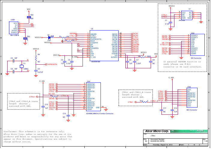
AU6438-BS 28PIN V1.00 读卡器原理图设计
VSS BS MSDATA1 MSDATA0 MSDATA2 INS MSDATA3 SCLK VCC VSS C12 MS Connector 1UF
B
C11 NC
SD/MMC/MMC4.0 Combo Connector
A
A
Disclaimer: This schematic is for reference only. Alcor Micro Corp. makes no warranty for the use of its products and bears no responsibility for any error that appear in this document. Specifications are subject to change without notice.
New release.
DATE
2012/08/16
BY
Nick
D
D
C
C
B
Байду номын сангаас
B
A
Alcor Micro Corp.
Title <Title> Size A Date:
5 4 3
A
Document Number AU6438-BS 28PIN Thursday, August 16, 2012
2
Rev 1.00 Sheet 2
1
of
2
600 DM DP U2 SDCDN R1 LED VCC3.3 330 CTRL1 CHIPRESETN R2 680 DP DM XI XO VCC1.8 C_V33 XI NC Y1 CHIPRESETN C3 0.47UF C_V33 C_V33 DATA2 DATA3 DATA4 SDCMD CTRL2 CTRL0 SD_V33 R9 DATA6 0 CTRL0_A 9 1 10 2 11 3 4 5 12 6 13 7 8 14 15 CN1 SDDATA2 SDDATA3 SDDATA4 CMD SDDATA5 VSS VDD CLK SDDATA6 VSS2 SDDATA7 SDDATA0 SDDATA1 SDCDN GND SDWP 1UF 0.1UF C4 C5 AU6438-BS 1UF 2.2UF NC 1 2 3 4 5 6 7 8 9 10 11 12 13 14 SDCDN CTRL1 GPON7 CHIPRESETN REXT V33APHY DP DM VSSAREG XI XO VSS V18 C_V33 DATA1 DATA0 CTRL3 DATA6 CTRL0 CTRL2 SDCMD DATA4 DATA3 DATA2 MSINS VSSHM V33 AVDD5V 28 27 26 25 24 23 22 21 20 19 18 17 16 15 C6 DATA1 DATA0 CTRL3 DATA6 CTRL0 CTRL2 SDCMD DATA4 DATA3 DATA2 MSINS VCC3.3 VCC R6 C7 1_0603 0.1UF
RT9610CGQW规格书

2
DS9610C-01 April 2016
RT9610C
Functional Block Diagram
VCC BOOT
POR UGATE EN VCC R PWM R Tri-State Detect Control Logic Shoot-Through Protection VCC LGATE GND PHASE
Features
Drives Two N-MOSFETs Adaptive Shoot-Through Protection 0.5Ω On-Resistance, 4A Sink Current Capability Supports High Switching Frequency Tri-State PWM Input for Power Stage Shutdown Output Disable Function Integrated Boost Switch Low Bias Supply Current VCC POR Feature Integrated
Ordering Information
RT9610C Package Type QW : WDFN-8L 2x2 (W-Type) Lead Plating System G : Green (Halogen Free and Pb Free)
Note : Richtek produVCC LGATE GND PWM
WDFN-8L 2x2
Functional Pin Description
Pin No. 1 2 3 4 Pin Name EN PHASE UGATE BOOT Pin Function Enable Pin. When low, both UGATE and LGATE are driven low and the normal operation is disabled. Switch Node. Connect this pin to the source of the upper MOSFET and the drain of the lower MOSFET. This pin provides a return path for the upper gate driver. Upper Gate Drive Output. Connect to the gate of high side power N-MOSFET. Floating Bootstrap Supply Pin for Upper Gate Drive. Connect the bootstrap capacitor between this pin and the PHASE pin. The bootstrap capacitor provides the charge to turn on the upper MOSFET. Control Input for Driver. The PWM signal can enter three distinct states during operation. Connect this pin to the PWM output of the controller. Ground. The exposed pad must be soldered to a large PCB and connected to GND for maximum power dissipation. Lower Gate Drive Output. Connect to the gate of the low side power N-MOSFET. Input Supply Pin. Connect this pin to a 5V bias supply. Place a high quality bypass capacitor from this pin to GND.
新编单片机原理与应用课后答案汇总

习题一参考答案1-1 假设某CPU 含有16根地址线,8根数据线,那么该CPU 的最大寻址能力为多少KB 答:CPU 的最大寻址能力为:K 6422261016=⋅= 1-2 在计算机里,一般具有哪三类总线请说出各自的特征(包括传输的信息类型、单向传输还是双向传输)。
答:1、数据总线,双向,输入输出数据信息;2、地址总线,单向,输出地址信息;3、控制总线,具体到某一根控制线为单向,输入或者输出控制信息;1-3 MCS-51系列单片机时钟周期、机器周期与指令周期这三者关系如何CISC 指令系统CPU 所有指令周期是否均相同答:时钟周期即为振荡周期,由外接晶振频率或外部输入的时钟频率决定,机器周期由12个时钟周期(或6个)构成,指令周期由1~4个机器周期构成;指令周期因具体指令不同而不同;1-4 计算机字长的含义是什么MCS-51单片机的字长是多少答:计算机字长是指CPU 一次能够处理的信息位长度;MCS-51单片机的字长是8位。
1-5 ALU 单元的作用是什么一般能完成哪些运算操作答:ALU 单元的作用是进行算术逻辑运算;算术运算主要是加、减、乘、除,逻辑运算主要是与、或、非、异或等。
1-6 CPU 内部结构包含了哪几部分单片机(MCU)芯片与通用微机CPU 有什么异同 答:CPU 主要包括算术逻辑单元ALU 、控制单元CU 和内部寄存器;单片机(MCU)芯片是在通用CPU 的基础上增加存储器、定时器/计数器、通信接口以及各种接口电路等构成。
1-7 在单片机系统中常使用哪些存储器答:包括程序存储器ROM 和数据存储器RAM 。
1-8 指令由哪几部分组成答:一般由操作码和操作数组成,部分指令只有操作码而无操作数。
1-9、什么是汇编语言指令为什么说汇编语言指令比机器语言指令更容易理解和记忆通过什么方式可将汇编语言程序转化为机器语言程序答:【1】用助记符表示的指令【2】因为在汇编语言指令中每条操作码、操作数都是用特定符号表示;而机器语言中的操作码和操作数均用二进制表示,没有明显特征【3】可通过专门的软件或手工查表方式1-10、汇编语言程序和汇编程序这两个术语的含义是否相同答:两者含义不同;1.汇编语言程序指由汇编语言指令构成的程序;2.汇编程序指将完成汇编语言指令转换为机器语言指令的程序1-11、什么是寻址方式对于双操作数指令来说,为什么不需要指定操作结果存放位置答:【1】确定指令中操作数所在存储单元地址的方式【2】在现代计算机系统中,对于双操作数指令,一般将指令执行后的结果放在第一个操作数(即目标操作数),这样可以减少指令码的长度1-12、指出下列指令中每一操作数的寻址方式答:【1】目标操作数为寄存器寻址,源操作数为立即数寻址【2】目标操作数为直接寻址,源操作数为寄存器寻址【3】目标操作数为直接寻址,源操作数为直接寻址【4】目标操作数为直接寻址,源操作数为寄存器间接寻址【5】寄存器寻址注:在单片机中,问到指令的寻址方式,既要答目标操作数的寻址方式,也要答源操作数的寻址方式,这与微机不同,请切记!1-13、单片机的主要用途是什么新一代8位单片机芯片具有哪些主要技术特征列举目前应用较为广泛的8位、32位单片机品种。
及其他系列芯片引脚图大全
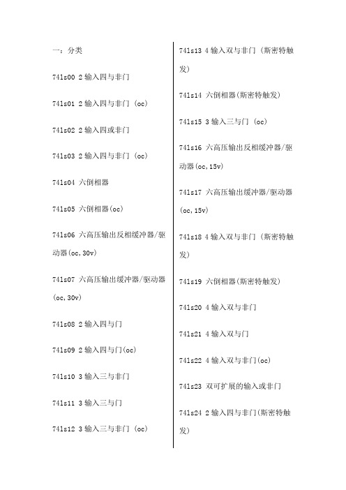
一:分类74ls00 2输入四与非门74ls01 2输入四与非门 (oc) 74ls02 2输入四或非门74ls03 2输入四与非门 (oc) 74ls04 六倒相器74ls05 六倒相器(oc)74ls06 六高压输出反相缓冲器/驱动器(oc,30v)74ls07 六高压输出缓冲器/驱动器(oc,30v)74ls08 2输入四与门74ls09 2输入四与门(oc)74ls10 3输入三与非门74ls11 3输入三与门74ls12 3输入三与非门 (oc) 74ls13 4输入双与非门 (斯密特触发)74ls14 六倒相器(斯密特触发) 74ls15 3输入三与门 (oc)74ls16 六高压输出反相缓冲器/驱动器(oc,15v)74ls17 六高压输出缓冲器/驱动器(oc,15v)74ls18 4输入双与非门 (斯密特触发)74ls19 六倒相器(斯密特触发) 74ls20 4输入双与非门74ls21 4输入双与门74ls22 4输入双与非门(oc)74ls23 双可扩展的输入或非门74ls24 2输入四与非门(斯密特触发)74ls25 4输入双或非门(有选通) 74ls26 2输入四高电平接口与非缓冲器(oc,15v)74ls27 3输入三或非门74ls28 2输入四或非缓冲器74ls30 8输入与非门74ls31 延迟电路74ls32 2输入四或门74ls33 2输入四或非缓冲器(集电极开路输出)74ls34 六缓冲器74ls35 六缓冲器(oc)74ls36 2输入四或非门(有选通) 74ls37 2输入四与非缓冲器74ls38 2输入四或非缓冲器(集电极开路输出74ls39 2输入四或非缓冲器(集电极开路输出)7 4ls40 4输入双与非缓冲器7 4ls41 bcd-十进制计数器7 4ls42 4线-10线译码器(bcd输入)7 4ls43 4线-10线译码器(余3码输入)7 4ls44 4线-10线译码器(余3葛莱码输入)7 4ls45 bcd-十进制译码器/驱动器7 4ls46 bcd-七段译码器/驱动器4ls47 bcd-七段译码器/驱动器74ls48 bcd-七段译码器/驱动器74ls49 bcd-七段译码器/驱动器(oc)74ls50 双二路2-2输入与或非门(一门可扩展)74ls51 双二路2-2输入与或非门74ls51 二路3-3输入,二路2-2输入与或非门74ls52 四路2-3-2-2输入与或门(可扩展)4ls53 四路2-2-2-2输入与或非门(可扩展)74ls53 四路2-2-3-2输入与或非门(可扩展)74ls54 四路2-2-2-2输入与或非门74ls54 四路2-3-3-2输入与或非门74ls54 四路2-2-3-2输入与或非门74ls55 二路4-4输入与或非门(可扩展)74ls60 双四输入与扩展74ls61 三3输入与扩展4ls62 四路2-3-3-2输入与或扩展器74ls63 六电流读出接口门74ls64 四路4-2-3-2输入与或非门 74ls65 四路4-2-3-2输入与或非门(oc)74ls70 与门输入上升沿jk 触发器74ls71 与输入r-s 主从触发器74ls72 与门输入主从jk 触发器74ls73 双j-k 触发器(带清除端)4ls74 正沿触发双d 型触发器(带预置端和清除端)74ls75 4位双稳锁存器74ls76 双j-k 触发器(带预置端和清除端)74ls77 4位双稳态锁存器74ls78 双j-k 触发器(带预置端,公共清除端和公共时钟端)74ls80 门控全加器74ls81 16位随机存取存储器4ls82 2位二进制全加器(快速进位) 4ls83 4位二进制全加器(快速进位)7 4ls84 16位随机存取存储器74ls85 4位数字比较器7 4ls86 2输入四异或门7 4ls87 四位二进制原码/反码/oi单元7 4ls89 64位读/写存储器7 4ls90 十进制计数器7 4ls91 八位移位寄存器74ls92 12分频计数器(2分频和6分频)7 4ls93 4位二进制计数器7 4ls94 4位移位寄存器(异步)7 4ls95 4位移位寄存器(并行io)7 4ls96 5位移位寄存器7 4ls97 六位同步二进制比率乘法器4ls100 八位双稳锁存器74ls103 负沿触发双j-k 主从触发器(带清除端)74ls106 负沿触发双j-k 主从触发器(带预置,清除,时钟)74ls107 双j-k 主从触发器(带清除端)74ls108 双j-k 主从触发器(带预置,清除,时钟)74ls109 双j-k 触发器(带置位,清除,正触发)4ls110 与门输入j-k 主从触发器(带锁定)74ls111 双j-k 主从触发器(带数据锁定)74ls112 负沿触发双j-k 触发器(带预置端和清除端)74ls113 负沿触发双j-k 触发器(带预置端)74ls114 双j-k 触发器(带预置端,共清除端和时钟端)74ls116 双四位锁存器74ls120 双脉冲同步器/驱动器4ls121 单稳态触发器(施密特触发)74ls122 可再触发单稳态多谐振荡器(带清除端)74ls123 可再触发双单稳多谐振荡器74ls125 四总线缓冲门(三态输出)74ls126 四总线缓冲门(三态输出)74ls128 2输入四或非线驱动器74ls131 3-8译码器4ls132 2输入四与非门(斯密特触发)74ls133 13输入端与非门74ls134 12输入端与门(三态输出)74ls135 四异或/异或非门74ls136 2输入四异或门(oc)74ls137 八选1锁存译码器/多路转换器74ls138 3-8线译码器/多路转换器 74ls139 双2-4线译码器/多路转换器4ls140 双4输入与非线驱动器74ls141 bcd-十进制译码器/驱动器 74ls142 计数器/锁存器/译码器/驱动器74ls145 4-10译码器/驱动器74ls147 10线-4线优先编码器74ls148 8线-3线八进制优先编码器74ls150 16选1数据选择器(反补输出)74ls151 8选1数据选择器(互补输出)4ls152 8选1数据选择器多路开关74ls153 双4选1数据选择器/多路选择器74ls154 4线-16线译码器74ls155 双2-4译码器/分配器(图腾柱输出)74ls156 双2-4译码器/分配器(集电极开路输出)74ls157 四2选1数据选择器/多路选择器74ls158 四2选1数据选择器(反相输出)4ls160 可预置bcd 计数器(异步清除)74ls161 可预置四位二进制计数器(并清除异步)74ls162 可预置bcd 计数器(异步清除)74ls163 可预置四位二进制计数器(并清除异步)74ls164 8位并行输出串行移位寄存器74ls165 并行输入8位移位寄存器(补码输出)4ls166 8位移位寄存器74ls167 同步十进制比率乘法器74ls168 4位加/减同步计数器(十进制)74ls169 同步二进制可逆计数器74ls170 4*4寄存器堆74ls171 四d 触发器(带清除端)74ls172 16位寄存器堆74ls173 4位d 型寄存器(带清除端)74ls174 六d 触发器4ls175 四d 触发器74ls176 十进制可预置计数器74ls177 2-8-16进制可预置计数器74ls178 四位通用移位寄存器74ls179 四位通用移位寄存器74ls180 九位奇偶产生/校验器74ls181 算术逻辑单元/功能发生器74ls182 先行进位发生器74ls183 双保留进位全加器4ls184 bcd-二进制转换器74ls185 二进制-bcd 转换器74ls190 同步可逆计数器(bcd,二进制)74ls191 同步可逆计数器(bcd,二进制)74ls192 同步可逆计数器(bcd,二进制)74ls193 同步可逆计数器(bcd,二进制)74ls194 四位双向通用移位寄存器4ls195 四位通用移位寄存器74ls196 可预置计数器/锁存器74ls197 可预置计数器/锁存器(二进制)74ls198 八位双向移位寄存器74ls199 八位移位寄存器74ls210 2-5-10进制计数器74ls213 2-n-10可变进制计数器74ls221 双单稳触发器74ls230 八3态总线驱动器4ls231 八3态总线反向驱动器74ls240 八缓冲器/线驱动器/线接收器(反码三态输出)74ls241 八缓冲器/线驱动器/线接收器(原码三态输出)74ls242 八缓冲器/线驱动器/线接收器74ls243 4同相三态总线收发器74ls244 八缓冲器/线驱动器/线接收器74ls245 八双向总线收发器4ls246 4线-七段译码/驱动器(30v)74ls247 4线-七段译码/驱动器(15v)74ls248 4线-七段译码/驱动器74ls249 4线-七段译码/驱动器74ls251 8选1数据选择器(三态输出)74ls253 双四选1数据选择器(三态输出)74ls256 双四位可寻址锁存器4ls257 四2选1数据选择器(三态输出)74ls258 四2选1数据选择器(反码三态输出)74ls259 8为可寻址锁存器74ls260 双5输入或非门74ls261 4*2并行二进制乘法器74ls265 四互补输出元件74ls266 2输入四异或非门(oc)74ls270 2048位rom (512位四字节,oc)4ls271 2048位rom (256位八字节,oc)74ls273 八d 触发器74ls274 4*4并行二进制乘法器74ls275 七位片式华莱士树乘法器74ls276 四jk 触发器74ls278 四位可级联优先寄存器74ls279 四s-r 锁存器74ls280 9位奇数/偶数奇偶发生器/较验器4ls28174ls283 4位二进制全加器74ls290 十进制计数器74ls291 32位可编程模74ls293 4位二进制计数器74ls294 16位可编程模74ls295 四位双向通用移位寄存器74ls298 四-2输入多路转换器(带选通)4ls299 八位通用移位寄存器(三态输出)74ls348 8-3线优先编码器(三态输出)74ls352 双四选1数据选择器/多路转换器74ls353 双4-1线数据选择器(三态输出)74ls354 8输入端多路转换器/数据选择器/寄存器,三态补码输出74ls355 8输入端多路转换器/数据选择器/寄存器,三态补码输出4ls356 8输入端多路转换器/数据选择器/寄存器,三态补码输出74ls357 8输入端多路转换器/数据选择器/寄存器,三态补码输出74ls365 6总线驱动器74ls366 六反向三态缓冲器/线驱动器74ls367 六同向三态缓冲器/线驱动器 74ls368 六反向三态缓冲器/线驱动器 74ls373 八d 锁存器4ls374 八d 触发器(三态同相)74ls375 4位双稳态锁存器74ls377 带使能的八d 触发器74ls378 六d 触发器74ls379 四d 触发器74ls381 算术逻辑单元/函数发生器 74ls382 算术逻辑单元/函数发生器 74ls384 8位*1位补码乘法器74ls385 四串行加法器/乘法器4ls386 2输入四异或门74ls390 双十进制计数器74ls391 双四位二进制计数器74ls395 4位通用移位寄存器74ls396 八位存储寄存器74ls398 四2输入端多路开关(双路输出)74ls399 四-2输入多路转换器(带选通)74ls422 单稳态触发器74ls423 双单稳态触发器 74ls440 四3方向总线收发器,集电极开路74ls441 四3方向总线收发器,集电极开路74ls442 四3方向总线收发器,三态输出74ls443 四3方向总线收发器,三态输出74ls444 四3方向总线收发器,三态输出74ls445 bcd-十进制译码器/驱动器,三态输出74ls446 有方向控制的双总线收发器74ls448 四3方向总线收发器,三态输出74ls449 有方向控制的双总线收发器74ls465 八三态线缓冲器74ls466 八三态线反向缓冲器74ls467 八三态线缓冲器74ls468 八三态线反向缓冲器74ls490 双十进制计数器74ls540 八位三态总线缓冲器(反向)74ls541 八位三态总线缓冲器74ls589 有输入锁存的并入串出移位寄存器74ls590 带输出寄存器的8位二进制计数器74ls591 带输出寄存器的8位二进制计数器74ls592 带输出寄存器的8位二进制计数器74ls593 带输出寄存器的8位二进制计数器74ls594 带输出锁存的8位串入并出移位寄存器74ls595 8位输出锁存移位寄存器74ls596 带输出锁存的8位串入并出移位寄存器74ls597 8位输出锁存移位寄存器74ls598 带输入锁存的并入串出移位寄存器74ls599 带输出锁存的8位串入并出移位寄存器74ls604 双8位锁存器74ls605 双8位锁存器74ls606 双8位锁存器74ls607 双8位锁存器74ls620 8位三态总线发送接收器(反相)74ls621 8位总线收发器74ls622 8位总线收发器74ls623 8位总线收发器74ls640 反相总线收发器(三态输出)74ls641 同相8总线收发器,集电极开路74ls642 同相8总线收发器,集电极开路74ls643 8位三态总线发送接收器74ls644 真值反相8总线收发器,集电极开路74ls645 三态同相8总线收发器74ls646 八位总线收发器,寄存器74ls647 八位总线收发器,寄存器74ls648 八位总线收发器,寄存器74ls649 八位总线收发器,寄存器74ls651 三态反相8总线收发器74ls652 三态反相8总线收发器74ls653 反相8总线收发器,集电极开路74ls654 同相8总线收发器,集电极开路74ls668 4位同步加/减十进制计数器74ls669 带先行进位的4位同步二进制可逆计数器74ls670 4*4寄存器堆(三态)74ls671 带输出寄存的四位并入并出移位寄存器74ls672 带输出寄存的四位并入并出移位寄存器74ls673 16位并行输出存储器,16位串入串出移位寄存器74ls674 16位并行输入串行输出移位寄存器74ls681 4位并行二进制累加器74ls682 8位数值比较器(图腾柱输出)74ls683 8位数值比较器(集电极开路)74ls684 8位数值比较器(图腾柱输出) 74ls685 8位数值比较器(集电极开路)74ls686 8位数值比较器(图腾柱输出)74ls687 8位数值比较器(集电极开路)74ls688 8位数字比较器(oc输出) 74ls689 8位数字比较器74ls690 同步十进制计数器/寄存器(带数选,三态输出,直接清除) 74ls691 计数器/寄存器(带多转换,三态输出)74ls692 同步十进制计数器(带预置输入,同步清除)74ls693 计数器/寄存器(带多转换,三态输出)74ls696 同步加/减十进制计数器/寄存器(带数选,三态输出,直接清除)74ls697 计数器/寄存器(带多转换,三态输出)74ls698 计数器/寄存器(带多转换,三态输出)74ls699 计数器/寄存器(带多转换,三态输出)74ls716 可编程模n十进制计数器74ls718 可编程模n十进制计数器LM12瓦运算放大器LM124 LM224 LM324 LM2902 低电压双路运算放大器LM324 低电压双路运算放大器LM129 LM329 精密电压基准芯片LM135 LM235 LM335 精密温度传感器芯片LM1458 LM1558 双运算放大器LM158 LM258 LM358 LM2904 低压双运算放大器LM18293 四通道推拉驱动器LM1868 调幅/调频收音机芯片LM1951 1安培固态开关LM2574 降阶式电压调节器LM1575 LM2575 1A 降阶式电压调节器LM2576 3A 3A 降阶式电压调节器LM1577 LM2577 降阶式电压调节器LM2587 5A 返馈开关式电压调节器LM1893 LM2893 载体电流收发器LM193 LM293 LM393 LM2903 双路低压低漂移比较器LM2907 LM2917 频率电压转换器LM101A LM201A LM301A 运算放大器芯片LM3045 LM3046 LM3086 晶体管阵列LM111 LM211 LM311 电压比较器LM117 LM317 三端可调式稳压器LM118 LM218 LM318 运算放大器LM133 LM333安培可调负电压调节器LM137 LM337 可调式三端负压稳压器LM34 精密华氏温度传感器LM342 三端正压稳压器LM148 LM248 LM348 / LM149 LM349 双LM741运算放大器LM35 精密摄氏温度传感器LM158 LM258 LM358 LM2904 低压双运算放大器LM150 LM350 3安培可调式电压调节器LM380 瓦音频放大器LM386 低压音频功率放大器LM3886 高性能68瓦音频功率放大器/带静音LM555 LM555C 时基发生器电路LM556 LM556C 双时基发生器电路LM565 相位跟随器LM567 音频译码器LM621 无刷电机换向器LM628 LM629精密位移控制器LM675功率运算放大器LM723 电压调节器LM741 运算放大器LM7805 LM78xx 系列稳压器LM7812 LM78xx 系列稳压器LM7815 LM78xx 系列稳压器LM78L00 三端正压调节器LM78L05 三端正压调节器LM78L09三端正压调节器LM78L12三端正压调节器LM78L15 三端正压调节器LM78L62 三端正压调节器LM78L82 三端正压调节器LM340 LM78Mxx 三端正压稳压器LM7905 三端负压调节器LM7912 三端负压调节器LM7915 三端负压调节器LM79Mxx三端负压调节器LF147 LF347 宽带J型场效应输入运算放大器LF351 宽带J型场效应输入运算放大器LF353 宽带J型场效应输入运算放大器LF444 双低压J型场效应输入运算放大器(1) 74LS00双输入四与非门,管脚图如附图1-27所示。
ZYNQ7000开发平台用户手册说明书

文档版本控制目录文档版本控制 (2)一、开发板简介 (6)二、AC7Z020核心板 (8)(一)简介 (8)(二)ZYNQ芯片 (9)(三)DDR3 DRAM (11)(四)QSPI Flash (14)(五)时钟配置 (16)(六)电源 (17)(七)结构图 (18)(八)连接器管脚定义 (19)三、扩展板 (23)(一)简介 (23)(二)CAN通信接口 (24)(三)485通信接口 (24)(四)千兆以太网接口 (25)(五)USB2.0 Host接口 (27)(六)USB转串口 (28)(七)AD输入接口 (29)(八)HDMI输出接口 (30)(九)MIPI摄像头接口(仅AX7Z020使用) (32)(十)SD卡槽 (33)(十一)EEPROM (34)(十二)实时时钟 (34)(十三)温度传感器 (35)(十四)JTAG接口 (36)(十五)用户LED灯 (36)(十六)用户按键 (37)(十七)扩展口 (38)(十八)供电电源 (40)(十九)底板结构图 (41)芯驿电子科技(上海)有限公司 基于XILINX ZYNQ7000开发平台的开发板(型号: AX7Z020B )2022款正式发布了,为了让您对此开发平台可以快速了解,我们编写了此用户手册。
这款ZYNQ7000 FPGA 开发平台采用核心板加扩展板的模式,方便用户对核心板的二次开发利用。
核心板使用XILINX 的Zynq7000 SOC 芯片的解决方案,它采用ARM+FPGA SOC 技术将双核ARM Cortex-A9 和FPGA 可编程逻辑集成在一颗芯片上。
另外核心板上含有2片共512MB 高速DDR3 SDRAM 芯片和1片256Mb 的QSPI FLASH 芯片。
在底板设计上我们为用户扩展了丰富的外围接口,比如2路CAN 通信接口,2路485通信接口,2路XADC 输入接口, 1路千兆以太网接口,1路USB2.0 HOST 接口,1路HDMI输出接口,Uart 通信接口,SD 卡座,40针扩展接口等等。
AIP1628 TM1628中微爱芯LED显示驱动芯片
AIP1628LED Driver ICProduct SpecificationSpecification Revision History :Version Data Description2010-01-A 2012-01-B1 2010-012012-01Replace the new templateIncrease in the number and history1/ 121、GENERAL DESCRIPTIONAIP1628是一款以1/5至1/8占空比驱动的LED 控制器。
10个段输出线,4个网格输出线,3个段/网格输出线,一个显示存储器,控制电路,键扫描电路都集成到一个芯片中,从而为单片机构建了高度可靠的外围设备。
通过三线串行接口连接到AIP1628。
AIP1628引脚采用28引脚SOP 封装,经过优化,可简化PCB 布局并节省成本。
Features● ● ● ● ● ● ● ● CMOS technologyLow power consumptionMultiple display modes (10 segment, 7 grid to 13 segment, 4 grid) Key scanning (10 x 2 Matrix) 8-step dimming circuitrySerial interface for clock, data input, data output, strobe pins Built-in RC oscillator: (450KHz±5%) Available in 28 pins, SOP2、BLOCK DIAGRAM AND PIN DESCRIPTION2.1、PIN CONFIGURATIONSNC 1 28 27 26GND DIO 2 CLK 3 STB 4 K1 5 GRID1 GRID225 GND 24 23 22GRID3 K2 6 GRID4 GNDVDD 7 SEG1/KS1 8 21 VDD SEG2/KS2 SEG3/KS3 9 20 19SEG14/GRID5 SEG13/GRID610 11 12 SEG4/KS4 18 SEG12/GRID7 17 SEG10/KS10 16 SEG9/KS9 15 SEG8/KS8SEG5/KS5 SEG6/KS6 13 14SEG7/KS72/ 122.2、PIN DESCRIPTION Pin No. Pin Name Description1 NCData input PinThis pin inputs serial data at the rising edge of the shift clock(starting from the lower bit)2 DIOData Output pin(N-Channel, Open-Drain)Clock input Pin .This pin reads serial data at the rising edge andoutputs data at the falling edge. 3 4CLKSTB Serial Interface Strobe PinThe data input after the STB has fallen is processed as a command.When this pin is “HIGH”, CLK is ignored. Key Data input Pins5,6 K1,K2 GND The data sent to these pins are latched at the end of the displaycycle.(Internal Pull-Low Resistor)Ground Pin22,25,28 SEG1/KS1~ Segment Output Pins(p-channel, open drain) 8~17 Also acts as the Key Source SEG10/KS10 SEG12/GRID7 ~Segment/Grid Output Pins18~20 SEG14/GRID6VDD GRID1~GRID47,21 26,27, 23,24Power SupplyGrid Output Pins 3、ELECTRICAL PARAMETER3.1、 ABSOLUTE MAXIMUM RATINGS (Unless otherwise stated, Ta=25℃, GND=0V)Characteristic Supply Voltage Input Voltage Symbol V DD V I1 ConditionsValue -0.3 to +7 -0.3 to V DD Unit V V +0.3I O1 Grid +200 Drive output current mA I O2 segment-50 -40~+80 Operating Temperature Topr Tstg ℃ ℃ -65~+150 Storage Temperature Power Dissipation P D T L400 250mW ℃Soldering Temperature10s 3.2、RECOMMENDED OPERATING RANGE (Ta= -20℃~+70℃,GND=0V )Parameter Symbol UnitMin. Typ. 5 - Max.5.5 Logic supply voltage High-level input voltage Low-level input voltage V DD 30.7V DD 0 V V VV IH V DD V IL - 0.3V DD3/ 12733-11-I3.3、ELECTRICAL CHARACTERISTICS3.3.1 DC CHARACTERISTICS (Ta= -20℃~+70℃,V DD=4.5V~5.5V ,GND=0V)Parameter Symbol ConditionsSeg1/KS1~Seg10/KS10,V O=V DD-2VSeg1/KS1~Seg10/KS10,V O=V DD-3V Min. Typ. Max. UnitmAI OH1 -20 -25 -40 High-level outputcurrentI OH2I OL1 -20804-301408-50 mAmAmALow-level output currentLow-level output currentGrid1~Grid4,V O= 0.3VV O=0.4V, DIO-- I DATASegmentHigh-level output I TOLSG current tolerance V O=V DD-3V,Seg1/KS1~- - 5 % Seg10/KS10Input current High-level voltage Low-level voltageI I V I=V DD/GND - --±1 uAV inputinputV IH CLK、DIO、STB 0.7V DDV IL CLK、DIO、STBCLK、DIO、STBNo load , display off----0.35-0.3V DD VVHysteresis Voltage V H -Dynamic dissipation Pull-down Resistor currentI DD dyn 5-mA RL K1~K2 - 10 KΩ3.3.2 SWITCHING CHARACTERISTICS(Ta= -20℃~+70℃,V DD=4.5V~5.5V)Parameter Oscillation frequency Propagation delay Symbolf OSCConditions Min-Typ450Max-UnitKHz t PLZt PZLCLK→DIOCL=15pF, R L=10KΩ----300100nsnsSeg1/KS1~Seg10/KS10Grid1~Grid4T TZH1 - - 2 usRise Time CL=300pFT TZH2 T THZ ----0.5 ususFall Time CL=300pF、Segn、Gridn 120Maximum clock frequencyInput FmaxC IDuty=50%-1---- MHzpF15capacitance3.3.3 TIMING CHARACTERISTICS(Ta= -20℃~+70℃,V DD=4.5V~5.5V)Parameter SymbolPWCLKPWSTBt SETUP Conditions Min4001Typ Max UnitnsClock pulse width STB pulse width Set-up time for data Hold time for data Propagation delay CLK to STB------------μs100100ns t HOLD ns t CLK STBt WAITCLK↑→STB↑CLK↑→CLK↓11----μsμsWait time4/ 124、FUNCTION DESCRIPTION4.1、Switching characteristic waveform4.2、DISPLAY MODE AND RAM ADDRESSData transmitted from an external device to AIP1628 via the serial interface are stored in the DisplayRAM and are assigned addresses. The RAM addresses of AIP1628 are given below in 8 bits unit.xxHL(Lower 4bits) xxHU(Higher 4 bits) xxHL(Lower 4bits) xxHU(Higher 4 bits)B0 B1 B2 B3 B4 B5 B6 B7 B0 B1 B2 B3 B4 B5 B6 B7 00HL02HL04HL06HL08HL0AHL0CHL00HU 01HL 01HU DIG1DIG2DIG3DIG4DIG5DIG6DIG702HU04HU06HU08HU0AHU0CHU03HL05HL07HL09HL0BHL0DHL03HU05HU07HU09HU0BHU0DHU5/ 124.3、KEY MATRIX & KEY INPUT DATA STORAGE RAMKey Matrix consists of 10 x 2 array as shown below:Each data entered by each key is stored as follows and read by a READ Command, starting from the last significant bit. When the most significant bit of the data (b0) has been read, the least significant bit of the next data (b7) is read, b6 and b7 do not care.B0 K1B1K2B2XB3K1B4K2B5XB6B7KS1KS3KS5KS7KS9KS2KS4KS6KS8KS10BYTE1BYTE2BYTE3BYTE4BYTE50 04.4、COMMANDS DESCRIPTION在STB引脚从高电平变为低电平状态之后,命令是通过DIO引脚输入到AIP1628的第一个字节(b0至b7)。
LT1930
123428fV IN , V OUT , SWA, SWB Voltage.......................–0.3 to 6V SWA, SWB Voltage, Pulsed, <100ns .........................7V SHDN, VC Voltage .........................................–0.3 to 6V FB Voltage ...................................–0.3 to (V OUT + 0.3V)Operating Temperature Range (Note 2)..–40°C to 85°C Storage Temperature Range..................–65°C to 125°CORDER PART NUMBER DD PART MARKING T JMAX = 125°C, θJA = 45°C/W,θJC = 3°C/WConsult LTC Marketing for parts specified with wider operating temperature ranges.LBBGABSOLUTE AXI U RATI GSW W WU PACKAGE/ORDER I FOR ATIOUUW (Note 1)ELECTRICAL CHARACTERISTICSNote 1: Absolute Maximum Ratings are those values beyond which the life of a device may be impaired.Note 2: The LTC3428E is guaranteed to meet performance specifications from 0°C to 70°C. Specifications over the –40°C to 85°C operatingtemperature range are assured by design, characterization and correlation with statistical process controls.The ● denotes the specifications which apply over the full operatingtemperature range, otherwise specifications are at T A = 25°C. V IN = 3.3V, V OUT = 5V unless otherwise noted.PARAMETERCONDITIONS MIN TYP MAX UNITSMinimum Startup Voltage 1.5 1.6V Quiescent Current, V OUT SHDN = V IN 100200µA Quiescent Current, V IN SHDN = V IN 1.32.0mA Shutdown Current SHDN = 0V 1µA Switching Frequency Per Phase ●0.8 1.0 1.2MHz FB Regulated Voltage ●1.2191.243 1.268V FB Input CurrentV FB = 1.24V150nA Error Amp Transconductance 170µS Output Adjust Voltage 1.65.25V NMOS Switch Leakage V SWA , V SWB = 5.5V, Per Phase 0.1 2.5µA NMOS Switch On Resistance V OUT = 5V, Per Phase 0.093ΩNMOS Current Limit Per Phase●2 2.5ASHDN Input Threshold ●0.40.8 1.5V SHDN Input Current 0.011µA Maximum Duty Cycle ●8087%Minimum Duty Cycle ●%Current Limit Delay to Output(Note 3)40nsNote 3: Specification is guaranteed by design and not 100% tested in production.Note 4: This IC includes overtemperature protection that is intended to protect the device during momentary overload conditions. Junctiontemperature will exceed 125°C when overtemperature protection is active.Continuous operation above the specified maximum operating junction temperature may impair device reliability.TOP VIEWDD PACKAGE10-LEAD (3mm × 3mm) PLASTIC DFN EXPOSED PAD MUST BE SOLDEREDTO GROUND PLANE ON PCB 10967845321PGNDB SWB V IN AGND FBPGNDA SWA V OUT SHDN V C11LTC3428EDD33428 G043428 G023428 G013428 G033428 G0710ns/DIV500ns/DIV500ns/DIV500ns/DIV100µs/DIVOutput Voltage Ripple with 22µF43428fPI FU CTIO SU U UPGNDA, PGNDB (Pins 1, 10, 11 (Exposed Pad)): Power Ground for the IC. Tie directly to local ground plane.SWB (Pin 2), SWA (Pin 9): Phase B and Phase A Switch Pins. The inductor and Schottky diodes for each phase are connected to these pins. Minimize trace length to reduce EMI.V OUT (Pin 3): Power Supply Output and Bootstrapped Power Source for the IC. Connect low ESR output filter capacitors from this pin to the ground plane.SHDN (Pin 4): Shutdown Pin. Grounding this pin shuts down the IC. Connect to a voltage greater than 1.5V to enable.TYPICAL PERFOR A CE CHARACTERISTICSU WP E A K C U R R E N T L I M I T (A )3.43.23.02.82.62.42.22.03428 G10TEMPERATURE (°C)–451555–25–5357595Peak Current Limit vs TemperatureV C (Pin 5): Error Amp Output. A frequency compensation network is connected to this pin to compensate the boost converter loop.FB (Pin 6): Feedback Pin. A resistor divider from V OUT is connected here to set the output voltage according to V OUT = 1.243 • (1 + R1 / R2)AGND (Pin 7): Signal Ground for the IC. Connect to ground plane near feedback resistor divider.V IN (Pin 8): Input Supply Pin. Bypass V IN with a low ESR ceramic capacitor of at least 4.7µF. X5R and X7R dielec-trics are preferred for their superior voltage and tempera-ture characteristics.56783428fTable 2. Capacitor Vendor InformationSupplier PhoneFaxWebsiteAVX (803) 448-9411(803) Sanyo (619) 661-9322(619) TDK (847) 803-6100(847) Murata(814) 237-1431(814) Taiyo Yuden (408) 573-4150(408) Output Diode SelectionFor high efficiency, a fast switching diode with low reverse leakage and a low forward drop is required. Schottky diodes are recommended for their low forward drop and fast switching times. When selecting a diode, it is important to remember that the average diode current in a boost converter is equal to the average load current: I D = I LOAD When selecting a diode, make sure that the peak forward current and average power dissipation ratings meet the application requirements. See Table 3 for a list of Schottky diode manufacturers. Example diodes are Philips PMEG1020, PMEG2010, On-Semi MBRA210, IR 10BQ015, Microsemi UPS120E, UPS315.Table 3. Diode Vendor InformationSupplier PhoneFaxWebsite Philips +31 40 27 Microsemi (949) 221-7100(949) On-Semi(602) 244-6600 International (310) 469-2161(310) RectifierThermal ConsiderationsTo deliver maximum power, it is necessary to provide a good thermal path to dissipate the heat generated within the LTC3428’s package. The large thermal pad on the IC underside can accomplish this requirement. Use multiple PC board vias to conduct heat from the IC and to a copper plane that has as much area as possible.APPLICATIO S I FOR ATIOW UUU If the junction temperature gets too high, the LTC3428 will stop all switching until the junction temperature drops to safe levels. The typical over temperature threshold is 150°C.Closing the Feedback LoopThe LTC3428 uses current mode control with internal,adaptive slope compensation. Current mode control elimi-nates the 2nd order pole in the loop response of voltage mode converters due to the inductor and output capacitor,simplifying it to a single pole response. The product of the modulator control to output DC gain and the error amp open-loop gain equals the DC gain of the system.G G G V V G V I G DC CONTROL EA REF OUTCONTROL IN OUTEA ==≈•••2100The output filter pole is given by:f I V C HzPOLE OUTOUT OUT=π••where C OUT is the output filter capacitor value. The output filter zero is given by:f R C HzZERO ESR OUT=12•••πwhere R ESR is the output capacitor equivalent series resistance.A complication of the boost converter topology is the right half plane (RHP) zero and is given by:f V R L V HzRHP IN O O=222••••π91011Information furnished by Linear Technology Corporation is believed to be accurate and reliable.However, no responsibility is assumed for its use. Linear Technology Corporation makes no represen-tation that the interconnection of its circuits as described herein will not infringe on existing patent rights.LTC3428123428fLinear Technology Corporation1630 McCarthy Blvd., Milpitas, CA 95035-7417(408) 432-1900 ● FAX: (408) 434-0507 ● © LINEAR TECHNOLOGY CORPORA TION 2004LT/TP 0804 1K • PRINTED IN USARELATED PARTSPART NUMBER DESCRIPTIONCOMMENTSLT1613550mA (I SW ), 1.4MHz, High Efficiency Step-Up 90% Efficiency, V IN : 0.9V to 10V, V OUT(MAX) = 34V, I Q = 3mA,DC/DC ConverterI SD <1µA, ThinSOT PackageLT1615/LT1615-1300mA/80mA (I SW ), High Efficiency Step-Up V IN : 1V to 15V, V OUT(MAX) = 34V, I Q = 20µA,DC/DC ConvertersI SD <1µA, ThinSOT PackageLT1618 1.5A (I SW ), 1.25MHz, High Efficiency Step-Up 90% Efficiency, V IN : 1.6V to 18V, V OUT(MAX) = 35V, I Q = 1.8mA,DC/DC ConverterI SD <1µA, MS PackageLT1930/LT1930A 1A (I SW ), 1.2MHz/2.2MHz, High Efficiency Step-Up High Efficiency, V IN : 2.6V to 16V, V OUT(MAX) = 34V,DC/DC ConvertersI Q = 4.2mA/5.5mA, I SD <1µA, ThinSOT PackageLT1946/LT1946A 1.5A (I SW ), 1.2MHz/2.7MHz, High Efficiency Step-Up High Efficiency, V IN : 2.45V to 16V, V OUT(MAX) = 34V, I Q = 3.2mA,DC/DC ConvertersI SD <1µA, MS8 PackageLT19611.5A (I SW ), 1.25MHz, High Efficiency Step-Up 90% Efficiency, V IN : 3V to 25V, V OUT(MAX) = 35V, I Q = 0.9mA,DC/DC ConverterI SD 6µA, MS8E PackageLTC3400/LTC3400B 600mA (I SW ), 1.2MHz, Synchronous Step-Up 92% Efficiency, V IN : 0.85V to 5V, V OUT(MAX) = 5V, I Q = 19µA/300µA,DC/DC ConverterI SD <1µA, ThinSOT PackageLTC34011A (I SW ), 3MHz, Synchronous Step-Up DC/DC Converter 97% Efficiency, V IN : 0.5V to 5V, V OUT(MAX) = 5.5V, I Q = 38µA,I SD <1µA, MS PackageLTC34022A (I SW ), 3MHz, Synchronous Step-Up DC/DC Converter 97% Efficiency, V IN : 0.5V to 5V, V OUT(MAX) = 5.5V, I Q = 38µA,I SD <1µA, MS PackageLTC34213A, 3MHz Synchronous Boost Converter 96% Efficiency, V IN : 0.5V to 4.5V, V OUT(MAX) = 5.5V, I Q = 12µA,with Output DisconnectI SD <1µA, QFN-24 PackageLTC34255A (I SW ), 8MHz, 4-Phase Synchronous Step-Up 95% Efficiency, V IN : 0.5V to 4.5V, V OUT(MAX) = 5.25V, I Q = 12µA,DC/DC ConverterI SD <1µA,QFN-32 PackageLTC3429600mA, 500kHz Synchronous Boost Converter 96% Efficiency, V IN : 0.5V to 4.4V, V OUT(MAX) = 5.5V, I Q = 20µA,with Output DisconnectI SD <1µA,ThinSOT PackageLTC34363A (I SW ), 1MHz, 34V Step-Up DC/DC Converter V IN : 3V to 25V, V OUT(MAX) = 34V, I Q = 0.9mA,I SD <6µA, TSSOP-16E PackageLTC345910V Micropower Synchronous Boost Converter 85% Efficiency, V IN : 1.5V to 5.5V, V OUT(MAX) = 10V, I Q = 10µA,I SD <1µA,ThinSOT PackageLT346485mA (I SW ), High Efficiency Step-Up DC/DC Converter V IN : 2.3V to 10V, V OUT(MAX) = 34V, I Q = 25µA,with Integrated Schottky and PNP DisconnectI SD <1µA,ThinSOT PackageNo R SENSE is a registered trademark of Linear Technology Corporation.。
第四章 内存及其与CPU的连接
三、主存储器设计
1、芯片选择 、 2、存储器芯片的基本地址 、 3、 存储器芯片的容量扩充 、 4、存储器芯片与 、存储器芯片与CPU连接 连接
1、芯片选择 、
连接, ①SRAM与CPU连接,不需要外围电路, 与 连接 不需要外围电路, 连接简单,用于小型控制系统。 连接简单,用于小型控制系统。 常用于大型系统, ②DRAM常用于大型系统,因为需要刷 常用于大型系统 新电路,比如PC机的内存条 机的内存条。 新电路,比如 机的内存条。 通常用于存放固定的系统程序。 ③ROM通常用于存放固定的系统程序。 通常用于存放固定的系统程序
CS
片选信号 H L L
OE
输出允许信号 × L ×
WE
写允许信号 × H L
A0~A10
方式 未选中 读出 写入 I/O 引脚 高阻 DOUT DI N
I/O0~I/O I/O~I/O7 CS W E OE 6116 +5V GND
常用的SRAM还有 还有6232,6264、62256,适用于 常用的 还有 , 、 , 较小系统。 较小系统。
(3)可靠性 (3)可靠性
存储器的可靠性用MTBF来衡量。 来衡量。 存储器的可靠性用 来衡量 MTBF即Mean Time Between 即 Failures —— 平均故障间隔时间,MBTF 平均故障间隔时间, 越长,表示可靠性越高。 越长,表示可靠性越高。
二、典型芯片举例
1、SRAM芯片 、 芯片HM 6116(简称 简称6116)— 芯片 简称 ) — 静态随机存取存储器,11条地址线,8位 静态随机存取存储器, 条地址线 条地址线, 位 数据线, 条控制线 两条电源线, 条控制线, 数据线,3条控制线,两条电源线,单片存 储容量2K× 储容量 ×8 。
AT28HC256产品资料
Features Array•Fast Read Access Time – 70 ns•Automatic Page Write Operation–Internal Address and Data Latches for 64 Bytes–Internal Control Timer•Fast Write Cycle Times–Page Write Cycle Time: 3 ms or 10 ms Maximum–1 to 64-byte Page Write Operation•Low Power Dissipation–80 mA Active Current–3 mA Standby Current•Hardware and Software Data Protection•DATA Polling for End of Write Detection•High Reliability CMOS Technology–Endurance: 104 or 105 Cycles–Data Retention: 10 Years•Single 5V ± 10% Supply•CMOS and TTL Compatible Inputs and Outputs•JEDEC Approved Byte-wide Pinout•Full Military and Industrial Temperature Ranges•Green (Pb/Halide-free) Packaging Option1.DescriptionThe AT28HC256 is a high-performance electrically erasable and programmable read-only memory. Its 256K of memory is organized as 32,768 words by 8 bits. Manufac-tured with Atmel’s advanced nonvolatile CMOS technology, the AT28HC256 offers access times to 70 ns with power dissipation of just 440 mW. When the AT28HC256 is deselected, the standby current is less than 5 mA.The AT28HC256 is accessed like a Static RAM for the read or write cycle without the need for external components. The device contains a 64-byte page register to allow writing of up to 64 bytes simultaneously. During a write cycle, the address and 1 to 64 bytes of data are internally latched, freeing the addresses and data bus for other oper-ations. Following the initiation of a write cycle, the device will automatically write the latched data using an internal control timer. The end of a write cycle can be detected access for a read or write can begin.Atmel’s 28HC256 has additional features to ensure high quality and manufacturability. The device utilizes internal error correction for extended endurance and improved data retention characteristics. An optional software data protection mechanism is available to guard against inadvertent writes. The device also includes an extra64 bytes of EEPROM for device identification or tracking.20007N–PEEPR–9/09AT28HC2562.128-lead TSOP Top View2.228-lead PGA Top View2.332-pad LCC, 32-lead PLCC Top ViewNote:PLCC package pins 1 and 17 are Don’t Connect.2.428-lead Cerdip/Flatpack/SOIC – Top View2.Pin ConfigurationsPin Name Function A0 - A14Addresses CE Chip Enable OE Output Enable WE Write Enable I/O0 - I/O7Data Inputs/Outputs NC No Connect DCDon’t Connect30007N–PEEPR–9/09AT28HC2563.Block Diagram4.Device Operation4.1Readdata stored at the memory location determined by the address pins is asserted on the outputs. control gives designers flexibility in preventing bus contention in their system.4.2Byte Writewrite cycle. The address is latched on the falling edge of CE or WE, whichever occurs last. will automatically time itself to completion. Once a programming operation has been initiated and for the duration of t WC , a read operation will effectively be a polling operation.4.3Page WriteThe page write operation of the AT28HC256 allows 1 to 64 bytes of data to be written into the device during a single internal programming period. A page write operation is initiated in the same manner as a byte write; the first byte written can then be followed by 1 to 63 additional bytes. Each successive byte must be written within 150 µs (t BLC ) of the previous byte. If the t BLC limit is exceeded the AT28C256 will cease accepting data and commence the internal programming operation. All bytes during a page write operation must reside on the same page as defined by the state of the A6 - A14 inputs. That is, for each WE high to low transition dur-ing the page write operation, A6 - A14 must be the same.The A0 to A5 inputs are used to specify which bytes within the page are to be written. The bytes may be loaded in any order and may be altered within the same load period. Only bytes which are specified for writing will be written; unnecessary cycling of other bytes within the page does not occur.4.4DATA PollingThe AT28HC256 features DATA Polling to indicate the end of a write cycle. During a byte or page write cycle an attempted read of the last byte written will result in the complement of the written data to be presented on I/O7. Once the write cycle has been completed, true data isduring the write cycle.40007N–PEEPR–9/09AT28HC2564.5Toggle Bitof a write cycle. During the write operation, successive attempts to read data from the device will result in I/O6 toggling between one and zero. Once the write has completed, I/O6 will stop toggling and valid data will be read. Testing the toggle bit may begin at any time during the write cycle.4.6Data ProtectionIf precautions are not taken, inadvertent writes to any 5-volt-only nonvolatile memory may occur during transition of the host system power supply. Atmel ® has incorporated both hard-ware and software features that will protect the memory against inadvertent writes.4.6.1Hardware ProtectionHardware features protect against inadvertent writes to the AT28HC256 in the following ways: (a) V CC sense – if V CC is below 3.8V (typical) the write function is inhibited; (b) V CC power-on delay – once V CC has reached 3.8V the device will automatically time out 5 ms typical) before allowing a write; (c) write inhibit – holding any one of OE low, CE high or WE high inhibits write initiate a write cycle.4.6.2Software Data ProtectionA software controlled data protection feature has been implemented on the AT28HC256. When enabled, the software data protection (SDP), will prevent inadvertent writes. The SDP feature may be enabled or disabled by the user; the AT28HC256 is shipped from Atmel with SDP disabled.SDP is enabled by the host system issuing a series of three write commands; three specific bytes of data are written to three specific addresses (refer to “Software Data Protection” algo-rithm). After writing the 3-byte command sequence and after t WC the entire AT28HC256 will be protected against inadvertent write operations. It should be noted, that once protected the host may still perform a byte or page write to the AT28HC256. This is done by preceding the data to be written by the same 3-byte command sequence.Once set, SDP will remain active unless the disable command sequence is issued. Power transitions do not disable SDP and SDP will protect the AT28HC256 during power-up and power-down conditions. All command sequences must conform to the page write timing spec-ifications. It should also be noted that the data in the enable and disable command sequences is not written to the device and the memory addresses used in the sequence may be written with data in either a byte or page write operation.After setting SDP, any attempt to write to the device without the three byte command sequence will start the internal write timers. No data will be written to the device; however, for the duration of t WC , read operations will effectively be polling operations.4.7Device IdentificationAn extra 64 bytes of EEPROM memory are available to the user for device identification. By raising A9 to 12V ± 0.5V and using address locations 7FC0H to 7FFFH the additional bytes may be written to or read from in the same manner as the regular memory array.4.8Optional Chip Erase ModeThe entire device can be erased using a 6-byte software code. Please see “Software Chip Erase” application note for details.50007N–PEEPR–9/09AT28HC256Notes: 1.X can be V IL or V IH .2.Refer to AC programming waveforms.3.V H = 12.0V ± 0.5V .5.DC and AC Operating RangeAT28HC256-70AT28HC256-90AT28HC256-12OperatingT emperature (Case)Ind.-40°C - 85°C-40°C - 85°C -40°C - 85°C Mil.-55°C - 125°C -55°C - 125°C V CC Power Supply5V ± 10%5V ± 10%5V ± 10%6.Operating ModesMode CE OE WE I/O Read V IL V IL V IH D OUT Write (2)V IL V IH V IL D IN Standby/Write Inhibit V IH X (1)X High ZWrite Inhibit X X V IH Write Inhibit X V IL X Output DisableX V IH X High Z Chip EraseV ILV H (3)V ILHigh Z 7.Absolute Maximum Ratings*T emperature under Bias ................................-55°C to +125°C *NOTICE:Stresses beyond those listed under “Absolute Maximum Ratings” may cause permanent dam-age to the device. This is a stress rating only and functional operation of the device at these or any other conditions beyond those indicated in the operational sections of this specification is not implied. Exposure to absolute maximum rating conditions for extended periods may affect device reliabilityStorage T emperature.....................................-65°C to +150°C All Input Voltages (including NC Pins)with Respect to Ground...................................-0.6V to +6.25V All Output Voltageswith Respect to Ground.............................-0.6V to V CC + 0.6V Voltage on OE and A9with Respect to Ground...................................-0.6V to +13.5V8.DC CharacteristicsSymbol Parameter ConditionMinMax Units I LI Input Load Current V IN = 0V to V CC + 1V 10µA I LO Output Leakage Current V I/O = 0V to V CC 10µA I SB1V CC Standby Current TTL CE = 2.0V to V CC A T28HC256-90, -123mA A T28HC256-7060mA I SB2V CC Standby Current CMOS CE = V CC - 0.3V to V CC A T28HC256-90, -12300µA I CC V CC Active Current f = 5 MHz; I OUT = 0 mA80mA V IL Input Low Voltage 0.8V V IH Input High Voltage 2.0V V OL Output Low Voltage I OL = 6.0 mA 0.45V V OHOutput High VoltageI OH = -4 mA2.4V60007N–PEEPR–9/09AT28HC25610.AC Read Waveforms (1)(2)(3)(4)Notes:1.CE may be delayed up to t ACC - t CE after the address transition without impact on t ACC .2.OE may be delayed up to t CE - t OE after the falling edge of CE without impact on t CE or by t ACC - t OE after an address changewithout impact on t ACC .3.t DF is specified from OE or CE whichever occurs first (C L = 5 pF).4.This parameter is characterized and is not 100% tested.9.AC Read CharacteristicsSymbol ParameterAT28HC256-70AT28C256-90AT28HC256-12Units MinMax MinMax MinMax t ACC Address to Output Delay 7090120ns t CE (1)CE to Output Delay 7090120ns t OE (2)OE to Output Delay 035040050ns t DF (3)(4)CE or OE to Output Float035040050ns t OHOutput Hold from OE, CE or Address, whichever occurred first00ns70007N–PEEPR–9/09AT28HC25611.Input Test Waveforms and Measurement Level12.Output Test LoadNote:1.This parameter is characterized and is not 100% tested.R F 13.Pin Capacitancef = 1 MHz, T = 25°C (1)Symbol Typ Max Units Conditions C IN 46pF V IN = 0V C OUT 812pFV OUT = 0V80007N–PEEPR–9/09AT28HC256Note:1.NR = No Restriction.15.AC Write Waveforms15.1WE Controlled15.214.AC Write CharacteristicsSymbol ParameterMin MaxUnits t AS , t OES Address, OE Setup Time 0ns t AH Address Hold Time 50ns t CS Chip Select Setup Time 0ns t CH Chip Select Hold Time 0ns t WP Write Pulse Width (WE or CE)100ns t DS Data Setup Time 50ns t DH , t OEH Data, OE Hold Time 0nst DV Time to Data Valid NR(1)90007N–PEEPR–9/09AT28HC25617.Page Mode Write Waveforms (1)(2)Notes: 1.A6 through A14 must specify the same page address during each high to low transition of WE (or CE).2.OE must be high only when WE and CE are both low.18.Chip Erase Waveforms16.Page Mode Write CharacteristicsSymbol ParameterMinTyp Max Units t WC Write Cycle Time (option available)A T28HC256510ms A T28HC256F23ms t AS Address Setup Time 0ns t AH Address Hold Time 50ns t DS Data Setup Time 50ns t DH Data Hold Time 0ns t WP Write Pulse Width 100ns t BLC Byte Load Cycle Time 150µs t WPHWrite Pulse Width High50nst S = t H = 5 µsec (min.)t W = 10 msec (min.)V H = 12.0V ± 0.5V100007N–PEEPR–9/09AT28HC25619.Software Data ProtectionEnable Algorithm (1)Notes:1.Data Format: I/O7 - I/O0 (Hex);Address Format: A14 - A0 (Hex).2.Write Protect state will be activated at end of writeeven if no other data is loaded.3.Write Protect state will be deactivated at end of writeperiod even if no other data is loaded.4.1 to 64 bytes of data are loaded.20.Software Data ProtectionDisable Algorithm (1)21.Software Protected Write Cycle Waveforms (1)(2)Notes:1.code has been entered.2.OE must be high only when WE and CE are both low.AT28HC256Notes:1.These parameters are characterized and not 100% tested.2.See “AC Read Characteristics” on page 6.23.Data Polling WaveformsNotes:1.These parameters are characterized and not 100% tested.2.See “AC Read Characteristics” on page 6.25.Toggle Bit WaveformsNotes: 1.Toggling either OE or CE or both OE and CE will operate toggle bit.2.Beginning and ending state of I/O6 will vary.3.Any address location may be used but the address should not vary.22.Data Polling Characteristics (1)Symbol Parameter Min TypMaxUnits t DH Data Hold Time 0ns t OEH OE Hold Time 0ns t OE OE to Output Delay (2)ns t WR Write Recovery Timens24.Toggle Bit Characteristics (1)Symbol Parameter Min TypMaxUnits t DH Data Hold Time 10ns t OEH OE Hold Time 10ns t OE OE to Output Delay (2)ns t OEHP OE High Pulse 150ns t WR Write Recovery Time0ns26.Normalized I CC GraphsAT28HC256 27.Ordering Information27.1Military Dual Marked Package27.1.1AT28HC256t ACC (ns)I CC (mA)Ordering Code Package Operation Range Active Standby90800.3A T28HC256-90DM/8835962-88634 03 XX28D6Military/883CClass B, Fully Compliant(-55°C to 125°C)A T28HC256-90FM/8835962-88634 03 ZX28FA T28HC256-90LM/8835962-88634 03 YX32LA T28HC256-90UM/8835962-88634 03 UX28U120800.3A T28HC256-12DM/8835962-88634 01 XX28D6 A T28HC256-12FM/8835962-88634 01 ZX28F A T28HC256-12LM/8835962-88634 01 YX32L A T28HC256-12UM/8835962-88634 01 UX28UPackage Type28D6 28-lead, 0.600" Wide, Non-windowed, Ceramic Dual Inline Package (Cerdip) 28F 28-lead, Non-windowed, Ceramic Bottom-brazed Flat Package (Flatpack) 32L 32-pad, Non-windowed, Ceramic Leadless Chip Carrier (LCC)28U 28-pin, Ceramic Pin Grid Array (PGA)OptionsBlank Standard Device: Endurance = 10K Write Cycles; Write Time = 10 msE High Endurance Option: Endurance = 100K Write CyclesF Fast Write Option: Write Time = 3 msNote: 1.No dual marking for this device.27.1.2AT28HC256E (1)t ACC (ns)I CC (mA)Ordering CodePackage Operation RangeActiveStandby90800.3A T28HC256E-90DM/88328D6Military/883CClass B, Fully Compliant(-55°C to 125°C)A T28HC256E-90FM/88328F A T28HC256E-90LM/88332L A T28HC256E-90UM/88328U 120800.3A T28HC256E-12DM/88328D6A T28HC256E-12FM/88328F A T28HC256E-12LM/88332L A T28HC256E-12UM/88328U27.1.3AT28HC256Ft ACC (ns)I CC (mA)Ordering Code Package Operation RangeActiveStandby90800.3A T28HC256F-90DM/8835962-88634 04 XX 28D6Military/883CClass B, Fully Compliant(-55°C to 125°C)A T28HC256F-90FM/8835962-88634 04 ZX 28F A T28HC256F-90LM/8835962-88634 04 YX 32L A T28HC256F-90UM/8835962-88634 04 UX 28U 120800.3A T28HC256F-12DM/8835962-88634 02 XX 28D6A T28HC256F-12FM/8835962-88634 02 ZX 28F A T28HC256F-12LM/8835962-88634 02 YX 32L A T28HC256F-12UM/8835962-88634 02 UX28UPackage Type28D6 28-lead, 0.600" Wide, Non-windowed, Ceramic Dual Inline Package (Cerdip)28F 28-lead, Non-windowed, Ceramic Bottom-brazed Flat Package (Flatpack)32L 32-pad, Non-windowed, Ceramic Leadless Chip Carrier (LCC)28U28-pin, Ceramic Pin Grid Array (PGA)OptionsBlank Standard Device: Endurance = 10K Write Cycles; Write Time = 10 ms E High Endurance Option: Endurance = 100K Write Cycles FFast Write Option: Write Time = 3 msAT28HC25627.2Industrial Green Package Option (Pb/Halide-free)27.3Ordering Information NotePrevious datasheets included the low power suffixes L, LE and LF on the AT28HC256 for 120 ns and 90 ns speeds. The low power parameters are now standard; therefore, the L, LE and LF suffixes are no longer required.27.2.1AT28HC256t ACC (ns)I CC (mA)Ordering Code Package Operation RangeActive Standby 70800.3A T28HC256-70JU 32J Industrial (-40°C to 85°C)A T28HC256-70SU 28S A T28HC256-70TU 28T 90800.3A T28HC256-90JU32J A T28HC256-90SU 28S A T28HC256-90TU 28T 120800.3A T28HC256-12JU32J A T28HC256-12SU 28S A T28HC256-12TU28T27.2.2AT28HC256Et ACC (ns)I CC (mA)Ordering Code Package Operation RangeActive Standby 90800.3A T28HC256E-90JU 32J Industrial (-40°C to 85°C)A T28HC256E-90SU 28S A T28HC256E-90TU 28T 120800.3A T28HC256E-12JU32J A T28HC256E-12SU 28S A T28HC256E-12TU28T27.2.3AT28HC256Ft ACC (ns)I CC (mA)Ordering Code Package Operation Range Active Standby 90800.3A T28HC256F-90JU 32J Industrial (-40°C to 85°C)A T28HC256F-90SU 28S A T28HC256F-90TU28TPackage Type32J 32-lead, Plastic J-leaded Chip Carrier (PLCC)28S 28-lead, 0.300" Wide, Plastic Gull Wing Small Outline (SOIC)28T28-lead, Plastic Thin Small Outline Package (TSOP)OptionsBlank Standard Device: Endurance = 10K Write Cycles; Write Time = 10 ms E High Endurance Option: Endurance = 100K Write Cycles FFast Write Option: Write Time = 3 ms27.4Die ProductsContact Atmel Sales for die sales options.AT28HC256 28.Packaging Information28.128D6 – Cerdip28.228F – FlatpackAT28HC256 28.332J – PLCC28.432L – LCCAT28HC256 28.528S – SOIC2128.628T – TSOP22AT28HC256AT28HC256 28.728U – PGA23Headquarters InternationalAtmel Corporation 2325 Orchard Parkway San Jose, CA 95131 USATel: 1(408) 441-0311 Fax: 1(408) 487-2600Atmel AsiaUnit 1-5 & 16, 19/FBEA Tower, Millennium City 5418 Kwun Tong RoadKwun Tong, KowloonHong KongTel: (852) 2245-6100Fax: (852) 2722-1369Atmel EuropeLe Krebs8, Rue Jean-Pierre TimbaudBP 30978054 Saint-Quentin-en-Yvelines CedexFranceTel: (33) 1-30-60-70-00Fax: (33) 1-30-60-71-11Atmel Japan9F, Tonetsu Shinkawa Bldg.1-24-8 ShinkawaChuo-ku, Tokyo 104-0033JapanTel: (81) 3-3523-3551Fax: (81) 3-3523-7581Product ContactWeb SiteTechnical Supportp_eeprom@Sales Contact/contactsLiterature Requests/literatureDisclaimer: The information in this document is provided in connection with Atmel products. No license, express or implied, by estoppel or otherwise, to any intellectual property right is granted by this document or in connection with the sale of Atmel products. EXCEPT AS SET FORTH IN ATMEL’S TERMS AND CONDI-TIONS OF SALE LOCATED ON ATMEL’S WEB SITE, ATMEL ASSUMES NO LIABILITY WHATSOEVER AND DISCLAIMS ANY EXPRESS, IMPLIED OR STATUTORY WARRANTY RELATING TO ITS PRODUCTS INCLUDING, BUT NOT LIMITED TO, THE IMPLIED WARRANTY OF MERCHANTABILITY, FITNESS FOR A PARTICULAR PURPOSE, OR NON-INFRINGEMENT. IN NO EVENT SHALL ATMEL BE LIABLE FOR ANY DIRECT, INDIRECT, CONSEQUENTIAL, PUNITIVE, SPECIAL OR INCIDEN-TAL DAMAGES (INCLUDING, WITHOUT LIMITATION, DAMAGES FOR LOSS OF PROFITS, BUSINESS INTERRUPTION, OR LOSS OF INFORMATION) ARISING OUT OF THE USE OR INABILITY TO USE THIS DOCUMENT, EVEN IF ATMEL HAS BEEN ADVISED OF THE POSSIBILITY OF SUCH DAMAGES. Atmel makes no representations or warranties with respect to the accuracy or completeness of the contents of this document and reserves the right to make changes to specifications and product descriptions at any time without notice. Atmel does not make any commitment to update the information contained herein. Unless specifically provided otherwise, Atmel products are not suitable for, and shall not be used in, automotive applications. Atmel’s products are not intended, authorized, or warranted for use as components in applications intended to support or sustain life.© 2009 Atmel Corporation. All rights reserved. Atmel®, logo and combinations thereof, and others are registered trademarks or trademarks of Atmel Corporation or its subsidiaries. Other terms and product names may be trademarks of others.。