NXP恩智浦 Freescale飞思卡尔后你需要知道的十件事
NXP恩智浦 Freescale飞思卡尔后你需要知道的十件事

NXP恩智浦Freescale飞思卡尔后你需要知道的十件事这两年,半导体行业似乎进入了多事之秋,收购战此起彼伏。
就在今年短短的3个月里,半导体行业并/收购案有:Avago Technologies 以6 亿美金价格收购无线网络公司Emulex Corp ELX.O,Maxlinear以2.87亿美元收购Entropic Communications,Lattice半导体则将以6亿美元价格收购Silicon Image。
3月初,恩智浦(NXP)以约118亿美元的价格并购飞思卡尔(Freescale),合并后的企业价值将超过400亿美元。
大公司的收购往往错综复杂,他们也有自己难以取舍的地方,有经济、情感、形象等多方面的考量。
这次并购会对恩智浦和飞思卡尔各自的产品、目标行业、半导体产业以及竞争对手带来哪些影响呢?我们目前还不能得到准确答案,但是希望能从对两家公司的十大对比中,让你看出一些端倪。
1.优势产品恩智浦微控制器、射频、传感器、无线(NFC)、模拟及电源。
杀手锏:NFC、智能卡IC。
飞思卡尔MCU&通信处理器、模拟技术与电源管理、射频、无线连接、传感器、软件和开发工具。
杀手锏:MCU&通信处理器(ARM MCU、ARM 应用处理器、QorIQ多核处理器、Power处理器、DSP)。
恩智浦+ 飞思卡尔不难发现,这两家的产品互补性很强,一个擅长连接,一个擅长处理和控制连接及其带来的数据。
恩智浦和飞思卡尔的专利数都约为10 000,可以从一个侧面反映他们的势均力敌。
而下面的专利“地图”,会让你直接感受到他们各自的强项。
图1 恩智浦与飞思卡尔的专利“地图” 在宣布合并交易时,恩智浦表示将出售自家高性能RF产品部门以避免主管机关审查问题,其实是因为NXP将保留原属于飞思卡尔、技术实力更强的RF部门,而不是他们自己的。
如果两家公司的RF业务合并,将有垄断全球高性能RF市场之虞,美国与欧洲的反垄断机构以及中国的商务部将审查这项合并交易。
2024年飞思卡尔直立车经验总结范本

2024年飞思卡尔直立车经验总结范本标题:2024年飞思卡尔直立车经验总结一、背景介绍2024年,飞思卡尔推出了全新的直立车型,为用户提供了更加方便快捷的出行方式。
在过去一年中,我作为一位直立车用户,深入体验了该车型的特点和性能,并在实际使用中积累了一些宝贵的经验。
在此,我将对2024年飞思卡尔直立车的使用体验进行总结和分享。
二、操作便捷性2024年飞思卡尔直立车在操作上非常简单便捷,只需借助生物感测技术和智能控制系统,倾斜身体即可控制车辆前进、后退、转弯等基本操作。
整个学习过程只需要一点点时间和耐心,我很快就能熟练地驾驶该车型,并在城市中自由穿梭。
三、平稳性和稳定性飞思卡尔直立车的底盘设计以及智能平衡系统保证了其在行驶过程中的平稳性和稳定性。
无论是面对起伏不平的道路、转弯时的侧倾还是突然的加速和减速,车辆都能够稳定地保持平衡,给用户带来安全感和舒适体验。
四、便携性和储存空间飞思卡尔直立车的设计非常轻便,便于携带。
其折叠式设计使得在不使用时可以方便地收纳在车上或者携带袋内,极大地方便了用户的出行。
此外,车辆后方还设计了一个储物空间,可以放置一些日常所需物品,提高了出行的便利性。
五、智能功能和安全性飞思卡尔直立车配备了丰富的智能功能,如防盗系统、智能导航、远程遥控等。
其中,智能导航系统能够为用户提供详细的路径规划和实时交通情况,帮助用户选择最佳路线。
而防盗系统能够有效地保护车辆的安全,减少偷盗风险。
六、电池续航能力和充电便利性飞思卡尔直立车的电池续航能力非常出色,一次充电能够满足日常通勤和出行的需求。
而且,充电也非常便利。
车辆配备了快速充电技术,只需几十分钟就能完成充电,用户无需长时间等待,大大提高了使用效率。
七、交通环保性作为一款电动交通工具,飞思卡尔直立车具有绿色环保的特点。
相比传统燃油车辆,它不产生废气污染和噪音,为改善空气质量和城市交通环境做出了贡献。
八、用户体验和建议总体而言,2024年飞思卡尔直立车给我带来了出乎意料的便捷和愉悦的用户体验。
2024年飞思卡尔直立车经验总结(3篇)

2024年飞思卡尔直立车经验总结关于飞思____智能车轨迹追踪竞赛飞思____智能车竞赛,由飞思____公司赞助,是一项全国本科院校共同参与的科技竞赛活动。
今年,安徽省有幸成为第____届省级赛区,我们专科院校也有幸参与其中。
基于专业的匹配,我们系在本专业中选拔了一些同学,我非常荣幸能与我的团队并肩合作。
由于我们学校初次参加,缺乏经验,指导老师正与我们一起逐步探索解决方案。
我们选择使用B型车进行光电寻迹任务。
根据任务需求,老师将其划分为几个关键模块(寻迹模块、电源模块、驱动模块、测速模块),我负责的是寻迹模块的构建。
起初,对于黑白寻迹,我仅感到“神秘”。
通过查阅资料和老师的指导,我理解了其寻迹原理。
这主要基于黑白颜色对光的反射差异(白色完全反射,黑色完全吸收)来识别黑白线。
由于我们之前未接触过传感器知识,对此领域略感模糊,因此我专门投入时间学习传感器,理解了其在电路中的功能。
接下来,我们面临材料选择的挑战,市场上的光电管种类繁多,各校使用的也不尽相同。
我们需要找到一款适合我们车辆的光电管。
我最初在网上找到一些电路图,并购买了一些光电管进行焊接,但结果并未达到预期。
我一度认为问题出在光电管上,但即使更换为光电发射与接收一体管,问题仍未解决。
在一段时间的停滞和反复试验后,我尝试调整了与接收管串联的电阻值(从10k改为100k),意外地提高了接收距离,达到十几厘米。
这仍不理想,因为为了防止光电管之间的相互影响,每个光电管都需要加上套管,而我们购买的光电管无法满足这一要求。
经过深入研究,查阅资料,以及反复实验,我们最终选择了____公司的光电管(型号)。
我想强调的是,他人的经验可以作为参考,但不一定适用于我们自身,就像我之前选择的光电管电路图,可能在某些情况下适用,但在我们的特定需求下并不理想。
在探索阶段,逐步实验始终是至关重要的。
确定光电管后,我们进入了电路焊接阶段。
我们借鉴了其他学校的经验,初步决定使用____来配置光电管。
芯片界的花式并购:电连技术如何接连境外收购

电连技术收购FTDI,是近些年半导体行业少有的、有望实现交易闭环的境外并购。
这起交易在建广资产的牵引下,以“上市公司+并购基金”的模式,先在境外收购FTDI,继而快速推出将其注入上市公司的计划。
但在注入方案中,电连技术却针对不同转让方,给出了至少4个收购价格。
其中显然有平衡不同投资人利益诉求、抓住发行股份定价窗口期,锁定发行价格等考量。
收购定价似乎已成为一门纯粹的“花式艺术”。
符胜斌/文芯片界的花式并购:电连技术如何接连境外收购通常来说,一起并购只有一个交易价格。
特殊情况下,收购价格会因为转让方股东承担的责任或风险不同而有所不同,比如上市公司收购时,有些转让方会因为承担了业绩承诺责任而能获得较高的价格,其他转让方只能获得较低的价格。
但电连技术(300679)近期拟进行的一场收购,颠覆了这个认知。
2022年6月27日,电连技术公告,拟收购USB桥接芯片龙头企业Future Technology Devices International Limited(未来科技芯片公司,简称“FTDI”)100%股权。
这起收购中,电连技术针对不同的转让方,至少给出了4个收购价格,或许还会有第5个。
但FTDI股东,在承担的责任或风险方面似乎并无差异。
令人不禁要问,这起交易的定价逻辑是什么?游戏的参与者这场并购交易共有18名参与者。
除电连技术外,17家转让方分别是由建广资产牵头设立的5家合伙企业的16位合伙人和1家境外股东。
根据电连技术的交易方案,16位合伙人将把其持有合伙企业的份额,悉数转让给电连技术,电连技术间接获得FTDI的80.2%股权。
与此同时,境外股东Stoneyford也向电连技术转让FTDI剩余19.8%股权。
交易完成后,FTDI将成为电连技术全资控股公司(图1)。
17家转让方中,建广资产是一家投资公司,专注于投资半导体行业,并取得一系列成绩。
比如借助恩智浦(NXP)和飞思卡尔(Freescale)合并的机会,收购了恩智浦的一系列业务等。
5G网络设备芯片的国产化现状及未来策略
5G网络设备芯片的国产化现状及未来策略2020年是中国5G大规模商用化元年,截至2020年11月,三大运营商已累计建成71.8万座基站,占全球比重接近7成。
未来三年,中国仍处于5G发展的导入期,5G建设逐渐向县城渗透,覆盖密度逐渐加深。
5G网络的建设需要采购大量设备,其中芯片器件所占成本高,技术难度最大。
在当前国际形势下,华为海思等国内芯片厂商陆续被美国政府加入“实体清单”,影响巨大。
未来,唯一的解决办法是提高国产化水平,实现安全可控的国产替代。
5G接入网由AAU、CU、DU构成,涉及到的芯片有基带芯片和射频芯片,其中射频芯片包含功率放大器、低噪声放大器、射频开关。
5G承载网全面采用光纤网,涉及到的芯片主要在光模块中,包含激光器芯片和探测器芯片。
5G核心网采用了SBA架构(Service Based Architecture),淘汰复杂的电信专用设备,采用X86服务器与虚拟软件,涉及到的芯片主要是X86服务器CPU和存储芯片。
综上,5G网络设备中的芯片如下图所示。
一、5G网络设备芯片的国产化现状1、5G基站基带芯片:华为、中兴具备设计能力,制造环节成瓶颈基带芯片是指用来将模拟信号转化为基带信号(数字信号),或对接收到的基带信号进行解码的芯片。
移动基站市场主要被华为、中兴、爱立信、诺基亚占领。
其中,华为海思在2019年1月推出了自行设计的天罡系列5G基站核心芯片,采用台积电7nm制程,华为5G基站的基带处理芯片已使用了天罡系列ASIC芯片。
中兴的5G基站使用中兴微电子自行设计的5G多模软基带芯片MSC3.0,采用的同样是台积电7nm制程,该芯片是中兴首款支持5G的基带芯片,集成了多种5G算法硬件加速IP,完备地支持5G现有协议标准,并具备后续协议演进的能力。
国外Marvell推出的5G基带处理器OCTEON Fusion可用于服务多扇区宏基站、微基站、智能射频头和分布式单元。
诺基亚与Marvell 在2020年3月就5G芯片技术达成合作协议,未来诺基亚的5G基站可能采用Marvell的产品。
飞思卡尔软件注意事项
飞思卡尔些许经验之软件设计------循迹基于电磁传感器,方向以及舵机调控基于B车模(仅供参考) 1、电感排布先说下各种排布类型电感的特点:左右竖直电感:对直角弯道十分敏感,可以清楚分辨出来十字弯与直角弯,但是对于曲率较大的S弯道会造成与直角弯道混淆。
在直角弯的时候左右电感差异非常大,可以较早判别出直角弯道,与左右水平电感结合可排除竖直电感对直角弯与大曲率S弯的误判左右水平电感:很适合判断直道以及小曲率弯道车子处在中心线的位置,但是对于曲率较大的S弯道与直角弯可能会造成左右判断相反的情况(即明明车子左偏赛道,但是根据电感差值却得出车子右偏赛道的结论),此时应该结合竖直电感或者斜电感来融合判断。
左右斜电感:对直角弯以及一切曲率的弯道敏感,缺点是过于敏感,若使用此电感差值作为误差偏移量会导致车子严重内切弯道,建议加入其余电感的权重,总体上不建议使用左右斜电感差值作为误差偏移量,但是作为一切弯道以及直道还有直角弯的方向判断是非常适合的。
另外应该注意的是此电感排布对于十字弯道会误判,这是由于十字弯道磁场排布的影响,但是可以与左右水平电感或左右竖直电感结合排除对十字弯道的误判。
中间水平电感:此电感非常适合用于误差偏移量的计算,即误差量=直道中心线值-实时值;用此方法得到的差值在弯道的时候只用稍稍加以处理就可平滑的咬中线过弯。
电感的排布基本上就这几种方式了,下边要说的是车子电感排布选择左右竖直电感加左右水平电感:本次比赛太原理工大学的电感排布,个人感觉过弯时对赛道误差偏移量的处理有较高要求,处理不好很有可能让车子严重内切赛道导致出界。
左右竖直电感加左右水平电感加中心水平电感:用中心水平电感获取赛道误差偏移量,方法参考上面的描述。
弯道方向判断用左右竖直电感。
直道方向判断用左右水平电感,直角预判用竖直电感,具体是若竖直电感左右差值达到一定程度了就看左右水平电感,若左右水平电感差值较小且左右电感值都较大,说明快要进入直角弯,否则说明在大曲率的S弯。
飞思卡尔半导体用户指南说明书

Freescale Semiconductor User’s Guide1OverviewThe Freescale Freedom development platform is a set of software and hardware tools for evaluation and development. It’s ideal for the rapid prototyping ofmicrocontroller-based applications. The Freescale Freedom KL26Z hardware (FRDM-KL26Z) is a capable and cost-effective design featuring a Kinetis L seriesmicrocontroller, the industry’s first microcontroller built on the ARM® Cortex™-M0+ core.FRDM-KL26Z can be used to evaluate the KL16 and KL26 Kinetis L series devices. It features a KL26Z128VLH4, a device boasting a maximum operating frequency of 48MHz, 128KB of flash, a full-speed USB controller, and numerous analog and digital peripherals. The FRDM-KL26Z hardware is form-factor compatible with the Arduino™ R3 pin layout, providing a broad range of expansion board options. The on-board interfaces include an RGB LED, a 6-axis digital sensor (combining a 3D accelerometer and 3Dmagnetometer), ambient light sensor, and a capacitive touch slider.The FRDM-KL26Z features the Freescale open standard embedded serial and debug adapter known as OpenSDA.Doc Number:FRDMKL26ZUGRev. 0, 10/2013Contents1.Overview . . . . . . . . . . . . . . . . . . . . . . . . . . . . . . . . . . . 12.Reference documents . . . . . . . . . . . . . . . . . . . . . . . . . 23.Getting started . . . . . . . . . . . . . . . . . . . . . . . . . . . . . . . 24.FRDM-KL26Z hardware overview . . . . . . . . . . . . . . 25.FRDM-KL26Z hardware description . . . . . . . . . . . . . 5FRDM-KL26Z User’s GuidebyFreescale Semiconductor, Inc.Reference documentsThis circuit offers several options for serial communications, flash programming and run-control debugging.2Reference documentsThe table below provides a list of reference documents for the FRDM-KL26Z hardware. All of these documents are available online at /FRDM-KL26Z.Table1. FRDM-KL26Z reference documentsFilename DescriptionFRDM-KL26Z Quick Start Package Quick Start Guide and supporting files for getting started with the FRDM-KL26Z FRDM-KL26Z User’s Guide This document—overview and detailed information for the FRDM-KL26ZhardwareFRDM-KL26Z Pinouts Spreadsheet of pin connections for all MCU pins. Includes pinout for the I/Oheaders, Arduino R3 compatibility chart, and OpenSDA MCU pinout.FRDM-KL26Z Schematics PDF schematics for the FRDM-KL26Z hardwareFRDM-KL26Z Design Package Zip file containing all design source files for the FRDM-KL26Z hardware OpenSDA User’s Guide Overview and instructions for use of the OpenSDA embedded debug circuit3Getting startedSee the FRDM-KL26Z Quick Start Package for step-by-step instructions to get started with the FRDM-KL26Z. See the Jump Start Your Design section on /FRDM-KL26Z for the Quick Start Package and software lab guides.4FRDM-KL26Z hardware overviewThe features of the FRDM-KL26Z include:•MKL26Z128VLH4 in a 64 LQFP package•Capacitive touch slider•FXOS8700CQ accelerometer and magnetometer•Tri-color (RGB) LED•Ambient light sensor•User push button•Flexible power supply options – USB, coin cell battery, external source•Battery-ready, power-measurement access points•Easy access to MCU I/O via Arduino™ R3 compatible I/O connectors•Programmable OpenSDA debug interface with multiple applications available including:—Mass storage device flash programming interface—P&E Debug interface provides run-control debugging and compatibility with IDE toolsFRDM-KL26Z hardware overview—CMSIS-DAP interface: new ARM standard for embedded debug interface—Data logging applicationFigure1 shows a block diagram of the FRDM-KL26Z design. The primary components and their placement on the hardware assembly are pointed out in Figure2.Figure1. FRDM-KL26Z block diagramFRDM-KL26Z hardware overview! (Figure2. FRDM-KL26Z feature call-outsFRDM-KL26Z hardware description5FRDM ‐KL26Z hardware description5.1Power supplyThere are multiple power supply options on the FRDM-KL26Z. It can be powered from either of the USB connectors, the VIN pin on the I/O header, an on-board coin cell battery, or an off-board 1.71-3.6V supply from the 3.3V pin on the I/O header. The USB and VIN supplies are regulated on-board using a 3.3V linear regulator to produce the main power supply. The other two sources are not regulated on-board. Table 2 provides the operational details and requirements for the power supplies.Table 2.Power supply requirementsNote that the OpenSDA circuit is only operational when a USB cable is connected and supplying power to J10. However, protection circuitry is in place to allow multiple sources to be powered at once.Figure 3 shows the schematic drawing for the power supply inputs and the on-board voltage regulator.Figure 3. Power supply schematicIn addition, regulated power can be supplied to J3 pin 10 from an external source through P5-9V_VIN by populating the board with an optional voltage regulator, e.g. a 7805 style regulator in a TO-220 package, thus providing a high current supply to external devices. To prevent voltage sag under a high load, C23,Supply Source Valid RangeOpenSDA Operational?Regulated on-board?OpenSDA USB (J7)5V Yes Yes KL26Z USB (J5)5V No Yes V in 4.3-9V No Yes 3.3V pin 1.71-3.6V No No Coin cell battery1.71-3.6VNoNoFRDM-KL26Z hardware descriptionC24, C25 & C28 should be populated with appropriately sized capacitors to match the regulator chosen. See Figure4.Figure4. Optional voltage regulator schematicTable3. FRDM-KL26Z power suppliesPowerDescriptionSupply NameP5-9V_VIN Power supplied from the V in pin of the I/O headers (J3 pin 16)P5V_SDA Power supplied from the OpenSDA USB connector (J10). A Schottky diode provides back drive protection.P5V_KL26Z Power supplied from the KL26Z USB connector (J6). A Schottky diode provides back drive protection P3V3_VREG Regulated 3.3V supply. Sources power to the P3V3 supply rail with an optional back drive protection Schottky diode.12P3V3_BATT Coin cell battery supply voltage. Sources power to the P3V3 supply rail with the option of adding a back drive protection Schottky diode.3P3V3Main supply rail for the FRDM-KL26Z assembly. May be sourced from P3V3_VREG, P3V3_BATT, or directly from the I/O headers (J3 pin 8).P3V3_KL26Z KL26Z MCU supply. Header J5 provides a convenient means for energy consumption measurements.4 P3V3_SDA OpenSDA circuit supply. Header J15 provides a convenient means for energy consumptionmeasurements.4P5V_USB Nominal 5V supplied to the I/O headers (J3 pin 10). Sourced from either the P5V_KL26Z or P5V_SDA supply through a back drive protection Schottky diode.FRDM-KL26Z hardware description5.2Serial and debug adapter (OpenSDA)OpenSDA is an open standard serial and debug adapter. It bridges serial and debug communications between a USB host and an embedded target processor as shown in Figure 5. The hardware circuit is based on a Freescale Kinetis K20 family microcontroller (MCU) with 128 KB of embedded flash and anintegrated USB controller. OpenSDA features a mass storage device (MSD) bootloader, which provides a quick and easy mechanism for loading different OpenSDA applications such as flash programmers, run-control debug interfaces, serial-to-USB converters, and more. See the OpenSDA User’s Guide for more details.Figure 5. OpenSDA high-level block diagramOpenSDA is managed by a Kinetis K20 MCU built on the ARM® Cortex™-M4 core. The OpenSDA circuit includes a status LED (D8) and a pushbutton (SW2). The pushbutton asserts a reset signal to the KL26Z target MCU. It can also be used to place the OpenSDA circuit into Bootloader mode. OpenSDA MCU RESET can be isolated from SW2 by cutting the trace between pins on J13. SPI and GPIO signals1By default the linear regulator, U1, is a 3.3V output regulator. However, this is a common footprint that would allow the user to modify the assembly to utilize an alternative device such as a 1.8V or 2.5V regulator. The KL26Z microcontroller has an operating range of 1.71V to 3.6V.2D2 is bypassed by J14. By default, the pins of J14 are shorted together, to reduce the voltage drop across D2. To use D2, cut the trace between the pins of J14.3If a coin cell battery is to be used, add a small amount of solder to the coin cell ground pad before adding the battery holder. Also, it is recommended to populate D1 as a protection diode when using a coin cell battery.4J5 and J15 are not populated by default. The two pins of these headers are in parallel with 0 Ω resistors. In addition, J5 is also in parallel with a 10 Ω resistor. To measure the energy consumption of the KL26Z, either a voltmeter or an ammeter may be used. To use a voltmeter, R3 (0 Ω) must be removed before connecting the voltmeter probes to the pins of J5. Both R3 and R2 (10 Ω) must be removed to measure current with an ammeter. For the OpenSDA MCU, energy consumption can be measured by removing R4 (0 Ω) and connecting ammeter probes to the pins of J15.FRDM-KL26Z hardware descriptionprovide an interface to the SWD debug port of the KL26Z. Additionally, signal connections are available to implement a UART serial channel. The OpenSDA circuit receives power when the USB connector J10 is plugged into a USB host.5.2.1Debug interfaceSignals with SPI and GPIO capability are used to connect directly to the SWD of the KL26Z. These signals are also brought out to a standard 10-pin (0.05”) Cortex Debug connector (J7). It is possible to isolate the KL26Z MCU from the OpenSDA circuit and use J7 to connect to an off-board MCU. To accomplish this, cut the trace on the bottom side of the PCB that connects J8 pin 1 to J8 pin 2. This will disconnect the SWD_CLK pin to the KL26Z so that it will not interfere with the communications to an off-board MCU connected to J7.Figure6. SWD debug connectorNote that J7 is not populated by default. A Samtec FTSH-105-02-F-D or compatible connector can be added to the J7 through-hole connector. A mating cable, such as a Samtec FFSD IDC cable, can then be used to connect from the OpenSDA of the FRDM-KL26Z to an off-board SWD connector.5.2.2Virtual serial portA serial port connection is available between the OpenSDA MCU and pins PTA1 and PTA2 of the KL26Z. Several of the default OpenSDA Applications provided by Freescale, including the MSD Flash Programmer and the P&E Debug Application, provide a USB communications device class (CDC) interface that bridges serial communications between the USB host and this serial interface on the KL26Z.5.3KL26Z microcontrollerThe target microcontroller of the FRDM-KL26Z is the KL26Z128VLH4, a Kinetis L series device in a 64 LQFP package. The KL26Z MCU features include:FRDM-KL26Z hardware description•32-bit ARM Cortex-M0+ core—Up to 48 MHz operation—Single-cycle fast I/O access port•Memories—128 KB flash—16 KB SRAM•System integration—Power management and mode controllers—Low-leakage wakeup unit—Bit manipulation engine for read-modify-write peripheral operations—Direct memory access (DMA) controller—Computer operating properly (COP) Watchdog timer•Clocks—Clock generation module with FLL and PLL for system and CPU clock generation—4 MHz and 32 kHz internal reference clock—System oscillator supporting external crystal or resonator—Low-power 1kHz RC oscillator for RTC and COP watchdog•Analog peripherals—16-bit SAR ADC w/ DMA support—12-bit DAC w/ DMA support—High speed comparator•Communication peripherals—Two 16-bit Serial Peripheral Interfaces (SPI)—USB dual-role controller with built-in FS/LS transceiver—USB voltage regulator—Two I2C modules—One low-power UART and two standard UART modules—One I2S module•Timers—One 6-channel Timer/PWM module—T wo 2-channel Timer/PWM modules—2-channel Periodic Interrupt Timer (PIT)—Real time clock (RTC)—Low-power Timer (LPTMR)—System tick timer•Human-Machine Interfaces (HMI)—General purpose input/output controllerFRDM-KL26Z hardware description—Capacitive touch sense input interface hardware module5.3.1Clock sourceThe Kinetis KL26 microcontrollers feature an on-chip oscillator compatible with three ranges of input crystal or resonator frequencies: 32-40 kHz (low freq. mode), 3-8 MHz (high frequency mode, low range) and 8-32 MHz (high frequency mode, high range). The KL26Z128 on the FRDM-KL26Z is clocked from an 8 MHz crystal.5.3.2USB interfaceThe Kinetis KL26 microcontrollers feature a dual-role USB controller with on-chip full-speed andlow-speed transceivers. The USB interface on the FRDM-KL26Z is configured as a full-speed USB device. J6 is the USB connector for this interface.Figure7. USB connector schematicIn order to enable USB host functionality on the FRDM-KL26Z, it is necessary to populate J9 and R8 as shown in Figure7. However, there is no electrical protection provided. Use the USB host functionality at your own risk.FRDM-KL26Z hardware description 5.3.3Serial portThe primary serial port interface signals are PTA1 and PTA2. These signals are connected to both the OpenSDA and to the J1 I/O connector. Note that the OpenSDA connection can be isolated from J1 by removing R13 & R14, if required.5.3.4ResetThe PTA20/RESET signal on the KL26Z128 is connected externally to a pushbutton, SW2, and also to the OpenSDA circuit. However, J13 has been provided to isolate the OpenSDA MCU from SW2. Isolating the RESET line allows a more accurate measurement of the target device’s power consumption in low-power modes. The reset button can be used to force an external reset event in the target MCU. The reset button can also be used to force the OpenSDA circuit into bootloader mode. See Section5.2, “Serial and debug adapter (OpenSDA), for more details.5.3.5DebugThe sole debug interface on all Kinetis L Series devices is a serial wire debug (SWD) port. The primary controller of this interface on the FRDM-KL26Z is the onboard OpenSDA circuit (see Section5.2, “Serial and debug adapter (OpenSDA)). However, an unpopulated 10-pin (0.05”) Cortex Debug connector, J7, provides access to the SWD signals. The Samtec FTSH-105-02-F-D or compatible connector can be added to the J7 through-hole debug connector to allow for an external debug cable to be connected.5.4Capacitive touch sliderTwo Touch Sense Input (TSI) signals, TSI0_CH9 and TSI0_CH10, are connected to capacitive electrodes configured as a touch slider. Freescale’s Touch Sense Software (TSS) provides a software library for implementing the capacitive touch slider.5.56-axis accelerometer and magnetometerA Freescale FXOS8700CQ low-power, six-axis accelerometer and magnetometer is interfaced through an I2C bus and two GPIO signals as shown in Table4. By default, the I2C address is 0x1D (SA0 pulled high).Table4. Accelerometer signal connectionsFX0S8700CQ KL26Z128SCL PTE24SDA PTE25INT1PTD0INT2PTD1FRDM-KL26Z hardware descriptionFigure 8. FXOS8700CQ schematic diagram5.6RGB LEDThree PWM-capable signals are connected to a red, green, blue LED, D7. The signal connections are shown in Table 5.Table 5. RGB LED signal connectionsFigure 9. RGB LED schematic diagramRGB LEDKL26Z128Red cathodePTE29Green cathodePTE31Blue cathodePTD511PTD5 is also connected to the I/O header on J2 pin 10 (also known as D13).FRDM-KL26Z hardware description5.7Ambient light sensorAn ambient light sensor is connected to ADC0_SE3 (PTE22). This sensor may be isolated from PTE22 by removing R36.5.8Input/Output connectorsThe KL26Z128VLK4 microcontroller is packaged in a 64-pin LQFP. Some pins are utilized in on-board circuitry, but many are directly connected to one of four I/O headers.The pins on the KL26Z microcontroller are named for their general purpose input/output port pin function. For example, the 1st pin on Port A is referred to as PTA1. The I/O connector pin names are given the same name as the KL26Z pin connected to it, where applicable.FRDM-KL26Z hardware descriptionNote that all pinout data is available in spreadsheet format in FRDM-KL26Z Pinouts. See Section2, “Reference documents” for details.5.9Analog reference voltageThe onboard ADC of the KL26Z128VLH4 MCU uses the Reference V oltage High (VREFH) and Reference V oltage Low (VREFL) pins to set high and low voltage references for the analog modules. On the FRDM-KL26Z, by default VREFH is attached to P3V3_KL26Z (3.3V Supply). VREFL is connected to GND. Figure10 illustrates this circuitry.Figure10. FRDM-KL26Z VREFH circuit schematicIf desired, VREFH can use a VDDA independent reference by adding R11 and a Zener diode (D6). R10 (0 Ω resistor) must be removed when implementing this option. Alternatively, VREFH can be attached to an external source through AREF by removing R10 and populating R9 with a 0 Ω resistor.5.10Arduino compatibilityThe I/O headers on the FRDM-KL26Z are arranged to allow compatibility with peripheral boards (known as shields) that connect to Arduino™ and Arduino-compatible microcontroller boards. The outer rows of pins (the even numbered pins) on the headers share the same mechanical spacing and placement as the I/O headers on the Arduino Revision 3 (R3) standard.FRDM-KL26Z hardware descriptionRefer to the FRDM-KL26Z Pinouts spreadsheet for a compatibility chart showing how all the functions of the KL26Z signals on the I/O connectors map to the pin functions available on the Arduino Uno R3.Document Number:FRDMKL26ZUG Rev. 010/2013Information in this document is provided solely to enable system and software implementers to use Freescale products. There are no express or implied copyright licenses granted hereunder to design or fabricate any integrated circuits based on the information in this document.Freescale reserves the right to make changes without further notice to any products herein. Freescale makes no warranty, representation, or guarantee regarding the suitability of its products for any particular purpose, nor does Freescale assume any liability arising out of the application or use of any product or circuit, and specifically disclaims any and all liability, including without limitation consequential or incidental damages. “Typical” parameters that may be provided in Freescale data sheets and/or specifications can and do vary in different applications, and actual performance may vary over time. All operating parameters, including “typicals,” must be validated for each customer application by customer’s technical experts. Freescale does not convey any license under its patent rights nor the rights of others. Freescale sells products pursuant to standard terms and conditions of sale, which can be found at the following address: /SalesTermsandConditions.How to Reach Us:Home Page:Web Support:/supportFreescale, the Freescale logo, and Kinetis are trademarks of FreescaleSemiconductor, Inc., Reg. U.S. Pat. & Tm. Off. ARM is the registered trademark ofARM Limited. ARM Cortex-M0+ is the trademark of ARM Limited. All other product orservice names are the property of their respective owners.© 2013 Freescale Semiconductor, Inc.。
FREESCALE 32位微控制器 MPC560xB C系列 車身和網關應用 说明书
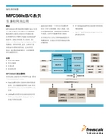
概述MPC560xB/C系列32位微控制器(MCU)包含了飛思卡爾用于汽車車身電子應用的最新集成器件。
這款先進的、經濟高效的主機處理器內核充分利用了Power Architecture® 的優勢,例如處理功能、片上存儲、模擬功能、時鐘系統及處理複雜控制和診斷系統所需的一些其他特性。
此外,這些可擴展功能由生態系統提供支持,它包括軟件驅動、操作系統和配置代碼,以幫助您快速實施您的設計。
應用• 中央車身控制器• 網關控制器• 車身應用• 舒適性應用MPC560xB/C的主要特性包括CAN、LIN及在車身網絡中實施一系列 不同功能所需的其他外設:• FlexCAN模塊同時支持FIFO和郵箱數據 存儲,適合控制器區域網絡(CAN)網關 管理事件驅動的總線流量和周期性總線流量• LINFlex模塊提供完全自動化的局域互聯 網絡(LIN)消息管理,從而減少了CPU負載干預和消息延遲• eMIOS定時器在一個非常靈活的模塊中結合了多個計數器源,如輸入捕捉、輸出比較和PWM功能;PWM功能支持移相信號輸出,以提高電磁兼容性能(EMC)• 交互觸發單元(CTU)同步PWM輸出信號與模數轉換,進而實現非常準確的診斷和控制功能• 可擴展的e200z0內核支持向更高性能解決方案的移植• 可兼容產品系列確保能重複使用軟件和工具基礎架構Color Indicator Bar/Volume no.32位微控制器MPC560xB/C系列車身和網關應用MPC560xB/C結構圖Color Indicator Bar/Volume no.Freescale 和Freescale 標識是飛思卡爾半導體公司的商標。
所有其他產品或服務的名稱是各自所有者的財產。
Power Architecture 和 字標、Power 和 標識、以及相關標記是.許可的商標和服務標記。
©飛思卡爾半導體公司2009年版權所有。
文件編號:MPC560XBFAMFS REV 0選型指南產品型號溫度範圍特性封裝速度MPC5604B -40°C to 125°C 512K Flash 、3 CAN 、3 SPI 、4 LINFlex 、64K DataFlash ®EEPROM 、32K RAM 、16位 定時器(多達56通道),10位ADC (多達36通道)100LQFP144LQFP 高達64 MHz MPC5604C -40°C to 125°C 512K Flash 、6 CAN 、3 SPI 、4 LINFlex 、64K DataFlash ® EEPROM 、32K RAM 、16位 定時器(多達28通道),10位ADC (多達16通道)100LQFP 高達64 MHz MPC5603B -40°C to 125°C 384K Flash 、2 CAN 、3 SPI 、4 LINFlex 、64K DataFlash ® EEPROM 、28K RAM 、16位 定時器(多達 56通道),10位ADC (多達36通道)100LQFP 144LQFP 高達64 MHz MPC5603C -40°C to 125°C 384K Flash 、6 CAN 、3 SPI 、4 LINFlex 、64K DataFlash ® EEPROM 、32K RAM 、16位 定時器(多達28通道),10位 ADC (多達16通道)100LQFP 高達64 MHz MPC5602B -40°C to 125°C 256K Flash 、2 CAN 、2 SPI 、3 LINFlex 、64K DataFlash ® EEPROM 、24K RAM 、16位 定時器(多達56通道),10位ADC (多達36通道)100LQFP 144LQFP 高達64 MHz MPC5602C-40°C to 125°C256K Flash 、6 CAN 、3 SPI 、4 LINFlex 、64K DataFlash ® EEPROM 、32K RAM 、16位 定時器(多達28通道),10位ADC(多達16通道)100LQFP高達64 MHz開發工具包部件編號描述定價*xPC560BKIT144SJDP 母板—(P/N xPC56XXMB) + 迷你模塊 (P/N xPC560BADPT144)(焊接)• 工具包包括母板、迷你模塊和P&E wiggler • 迷你模塊/工具包有插槽式(約450美元)和焊接式(約350美元)兩個版本;最終生產版本將是焊接式• 迷你模塊可以單獨使用• 焊接MCU 的最終生產計劃用于Rev A 版硅片$360 美元xPC560BKIT100SJDP 母板—(P/N xPC56XXMB) + 迷你模塊 (P/N xPC560BADPT100)(焊接)• 工具包包括母板、迷你模塊和P&E wiggler • 迷你模塊有插槽式(約450美元)和焊接式(約350美元)兩個版本;最終生產版本將是焊接式• 迷你模塊可以單獨使用• 焊接MCU 的最終生產計劃用于Rev A 版硅片$350 美元xPC560BKIT208SJDP 母板—(P/N xPC56XXMB) + 迷你模塊 (P/N xPC560BADPT208)(焊接)• 工具包包括母板、迷你模塊和P&E wiggler • 迷你模塊/工具包有插槽式(約450美元)和焊接式(約350美元) 兩個版本;最終生產版本將是焊接式• 迷你模塊可以單獨使用• 焊接MCUs 的最終生產計劃用于Rev A 版硅片$350 美元MPC5604BDEMOMPC5604DEMO 板卡• 低成本板卡• USB 供電• CAN/LIN 收發器• I/O 接入• 串連到USB 轉換器$100 美元144LQFP 至208MAPBGA—Nexus 接入板適配器允許客戶以144 LQFP 封裝使用208 MAPBGA 允許客戶使用Nexus 2.0功能*製造商建議零售價。
- 1、下载文档前请自行甄别文档内容的完整性,平台不提供额外的编辑、内容补充、找答案等附加服务。
- 2、"仅部分预览"的文档,不可在线预览部分如存在完整性等问题,可反馈申请退款(可完整预览的文档不适用该条件!)。
- 3、如文档侵犯您的权益,请联系客服反馈,我们会尽快为您处理(人工客服工作时间:9:00-18:30)。
NXP恩智浦Freescale飞思卡尔后你需要知道的十件事这两年,半导体行业似乎进入了多事之秋,收购战此起彼伏。
就在今年短短的3个月里,半导体行业并/收购案有:Avago Technologies 以6 亿美金价格收购无线网络公司Emulex Corp ELX.O,Maxlinear以2.87亿美元收购Entropic Communications,Lattice半导体则将以6亿美元价格收购Silicon Image。
3月初,恩智浦(NXP)以约118亿美元的价格并购飞思卡尔(Freescale),合并后的企业价值将超过400亿美元。
大公司的收购往往错综复杂,他们也有自己难以取舍的地方,有经济、情感、形象等多方面的考量。
这次并购会对恩智浦和飞思卡尔各自的产品、目标行业、半导体产业以及竞争对手带来哪些影响呢?我们目前还不能得到准确答案,但是希望能从对两家公司的十大对比中,让你看出一些端倪。
1.优势产品恩智浦微控制器、射频、传感器、无线(NFC)、模拟及电源。
杀手锏:NFC、智能卡IC。
飞思卡尔MCU&通信处理器、模拟技术与电源管理、射频、无线连接、传感器、软件和开发工具。
杀手锏:MCU&通信处理器(ARM MCU、ARM 应用处理器、QorIQ多核处理器、Power处理器、DSP)。
恩智浦+ 飞思卡尔不难发现,这两家的产品互补性很强,一个擅长连接,一个擅长处理和控制连接及其带来的数据。
恩智浦和飞思卡尔的专利数都约为10 000,可以从一个侧面反映他们的势均力敌。
而下面的专利“地图”,会让你直接感受到他们各自的强项。
图1 恩智浦与飞思卡尔的专利“地图” 在宣布合并交易时,恩智浦表示将出售自家高性能RF产品部门以避免主管机关审查问题,其实是因为NXP将保留原属于飞思卡尔、技术实力更强的RF部门,而不是他们自己的。
如果两家公司的RF业务合并,将有垄断全球高性能RF市场之虞,美国与欧洲的反垄断机构以及中国的商务部将审查这项合并交易。
重点:微控制器(MCU)恩智浦+飞思卡尔后的新公司将在通用微控制器(MCU)市场成为紧追第一大供应商的排名第二的大厂商(如图2所示),目前恩智浦的微控制器业务规模只有飞思卡尔的五分之一。
而VDC的数据则显示,合并后的恩智浦在该市场的占有率为17%,第一大供应商瑞萨市占率则有25%。
无论怎么算,MCU市场都是一个高度分散且竞争激烈的领域,当所有的厂商都采用ARM 核,要做到产品差异化越来越困难。
至于具体产品的谁去谁留,真不好说,特别是对于“严重重合”的处理器(如基于Cortex-M0/M4的MCU),是保留“亲生子”还是“大义灭亲”,不妨先凑个热闹分析一下。
图2 NXP官方提供的MCU市场占有率排名恩智浦恩智浦有最广泛的32位ARM MCU产品组合之一,有多达400多款MCU,并且使用同样的LPC开发套件。
其中,入门级有3个系列,高性能有12个系列,还有基于80C51的8/16 bit MCU(3个系列),用于计量等特殊应用的有三个系列。
恩智浦微控制器主要的特点:蓝牙、CAN、显示、以太网、电机控制、传感器处理、USB、无线(基于IEEE802.15.4的无线网络系统)。
LPC微控制器的定位是探索差异恩智浦基于ARM核的MCU 分别有:Cortex-M0+/M0(共124款产品)、Cortex-M3 (共117款产品)、Cortex-M4/M4F (共9款产品)、Cortex-M0&M4F (共55款产品)、Cortex-M0+&M4F(共5款产品)。
飞思卡尔飞思卡尔在ARM MCU、ARM应用处理器、QorIQ多核处理器、Power处理器和DSP都算得上佼佼者。
2104年第三季度是飞思卡尔创纪录的一个季度,销售额达到2.51亿美元。
这些还只是工业、通用MCU市场,包括i.MX应用处理器方面的营业额,但并不包括汽车MCU的业务。
知名的产品系列(包括64 bit&32 bit)有:Kinetis(基于Cortex-M0+/M4/M7)、i.MX(基于Cortex-A8/A9)、QorIQ处理平台(基于Power Architecture和Cortex-A7/A9/A53/57,网络)、PowerQUICC处理器(基于Power Architecture,联网设备)。
在被问到未来合并后是否会调整两家公司的ARM Cortex-M微控制器产品线时,NXP CEO Clemmer表示这些细节恩智浦还需要等到合并完成之后再处理,也就是“产品选择”。
在处理器部分,Clemmer先指出飞思卡尔已经有处理器平台,又很快补充:“我认为处理器是一个我们应该与伙伴进行合作的技术领域。
” 2.优势领域恩智浦涉及汽车、消费、工业、医疗、照明、安全交易、RFID、无线基础设施、物联网等诸多领域。
最牛的:安全交易(2014年总收入11亿美元)、汽车(2014年总收入14亿美元)。
安全和连接的交叉领域将带来更多的驱动力。
在一些新兴应用中,安全连接设备领域的增长率是最快的,高达81%,其2014年为NXP贡献了10亿美元。
飞思卡尔涉及汽车、消费、工业、医疗、网络、智能电网、无线基础设施、物联网、电机控制、数据连接、智能能源。
最牛的:汽车信息娱乐、网络、物联网。
飞思卡尔2014年在全球范围内的增长主要来自IoT和智能互联增长的贡献。
其实不管是汽车、网络产品,飞思卡尔都尝试把它们往物联网上去靠拢。
从边缘节点到网关,从数据中心到联网设备,飞思卡尔为物联网提供了完整的产品和解决方案。
恩智浦+ 飞思卡尔合并后,其互补的产品系列将是物联网解决方案的理想选择,包括安全性、MCU、软件、连接和广泛的客户群基础。
重点:汽车恩智浦实现汽车互联恩智浦一直专注于汽车互联上应用,包括:汽车娱乐、车联网、安全汽车接入、安全V2X 通信(车对车信息交互)、雷达。
NXP在汽车电子上做了些什么呢?简明扼要是汽车各个部件都可以用的模拟器件,繁杂地来表述就有:收发信机、RF、RFID的可追溯性、计时设备、汽车MOSFET (446)、音频放大器、汽车门禁与防盗IC、多媒体、调幅/调频收音机和音频、多标准数字收音机(8)、传感器、汽车照明、分立器件、逻辑、显示器和仪表盘。
恩智浦的汽车AM/FM收音机芯片在28台车用音响中有27台选用,客户涵盖一阶汽车电子供应商与各大车厂。
NXP有调谐器与DSP, 一旦飞思卡尔的应用处理器加入,将让新一代的恩智浦汽车音讯平台成为功能更完整的汽车信息娱乐系统。
图3 恩智浦实现汽车互联汽车正从单一交通工具演变成个性化移动信息中心。
恩智浦通过实现可靠、安全和高效的车内、车外电子通信,帮助推动这一变化。
其在广播接收、车载网络和RF加密技术方面的能力已经得到证实,另外还有不断增加的IC 解决方案系列——可用于远程信息处理、802.11p汽车无线技术和NFC应用。
所有这些均得到了领先的逻辑、接口产品、磁阻传感器、小信号分立器件、固态照明驱动器和标准MOSFET的支持。
解决方案:汽车照明、自动传输、车身控制/中央闸道模组、制动系统、汽车收音机、汽车互联、电子助力转向系统、汽油引擎控制、音响本体、仪表组、导航系统、被动无钥门禁、启停系统。
飞思卡尔实现汽车控制和信息处理在处理器方面的车用级主打产品包括:Vybrid控制器(基于ARM Cortex-A5/M4,汽车、工业应用)、S32微控制器(4个Coretx-A53核,汽车应用)、MAC57DXXX汽车微控制器(Cortex-M0+/M4/M5,仪表盘)、i.MX应用处理器(基于Cortex-A8/A9,汽车多媒体)。
说到汽车信息娱乐系统,i.MX的口碑那在业界是杠杠的,据悉,全球前十名的OEM汽车原厂都使用了飞思卡尔i.MX应用处理器。
i.MX已经好几年前就到第六代了,其他产品系列也在不断创新。
飞思卡尔Kinetis EA系列MCU是Kinetis汽车系列中的第一款产品,它专为中国市场开发。
此外还有专为汽车仪表板打造的三核MAC57D5xx以及非常优秀的车用视觉SoC(S32V)。
恩智浦+ 飞思卡尔合并之后的恩智浦将会成为“无人能及”的全球第一大汽车半导体厂商。
根据两家公司在汽车半导体市场的占有率来计算,合并后的恩智浦与飞思卡尔将成为一家在2014年营收总计40亿美元的厂商,比排名在后的瑞萨(Renesas)还至少高出10亿美元。
从以上对比可以看出,恩智浦与飞思卡尔的汽车芯片业务最大不同之处,是前者聚焦连结界面与安全性──主要应用是连网汽车直接暴露在外的区域,而飞思卡尔的强项则在于引擎控制与传动动力系统。
IHS Technolog车用半导体市场首席分析师Luca DeAmbroggi表示,两家公司的结合将能为各种高成长应用提供完整汽车半导体解决方案,包括汽车信息娱乐系统、高级驾驶辅助系统(ADAS)、车用连网技术,以及车内安全技术、混合动力/电动车等热门新领域。
恩智浦与飞思卡尔也都在推动连网汽车安全性技术的问题。
飞思卡尔的安全性是以软件技术实现的;恩智浦则是开发硬件的安全性,所利用的就是恩智浦擅长的身份识别与金融卡安全晶片技术。
此外飞思卡尔的雷达技术很强,恩智浦在今年MWC也宣布开发了一款CMOS制程小型雷达晶片,除了飞思卡尔的雷达方案,汽车业者现在也能为车辆添加数个小型雷达系统,增强车辆安全性。
合并之后,NXP在汽车半导体领域有着“舍我其谁”的气派了,不单在量上,相信质也会有更大的飞跃。
图4 NXP提供的预计合并后的汽车半导体市场占有率 3.朋友圈-开放的模式你可能每天都在刷微信的朋友圈,每个人看朋友圈的目的并不一样,但是都是怀着开放的心态在玩转朋友圈。
公司也是一样的,单打独斗的时代已经终结,没有永远的敌人,哪怕在某方面存在竞争,只要有好机会,谁也不会拒绝合作。
因此“生态系统”这几年常常在半导体等科技公司中被提及,其实就是他们的朋友圈,大家互相合作,构造一个生机勃勃的生态系统。
恩智浦就在去年,NXP选择了与腾讯、阿里巴巴、谷歌、百度、中国移动这类公司挂钩,推广其NFC技术在智能家居(物联网的重要一环)中的应用,NXP将联合产业链合作伙伴推出全新智能家居套件。
此外,NXP MCU的解决方案也尝试与生态系统中其他成员合作。
例如NXP新MCU配套的开发板LPCXpresso54102就与博世、Maxim展开合作。
飞思卡尔飞思卡尔庞大的圈子,飞思卡尔一位高层曾经表示,飞思卡尔每年花大量的钱在标准和生态圈、不同联盟的建设中,例如,与谷歌一起建立的物联网联盟Thread。
光从每年FTF的参会企业就能看出飞思卡尔朋友圈的庞大了。
收购前,飞思卡尔曾打算与云服务公司开展合作。