Chapter 11-Bandgap References
低成本多路输出CMOS带隙基准电压源设计
低成本多路输出CMOS带隙基准电压源设计蔡元;张涛【摘要】在传统Brokaw带隙基准源的基础上,提出一种采用自偏置结构和共源共栅电流镜的低成本多路基准电压输出的CMOS带隙基准源结构,省去了一个放大器,并减小了所需的电阻阻值,大大降低了成本,减小了功耗和噪声.该设计基于华虹1 μm的CMOS工艺,进行了设计与仿真实现.Cadence仿真结果表明,在-40~140℃的温度范围内,温度系数为23.6 ppm/℃,静态电流为24μA,并且能够产生精确的3V,2V,1V和0.15V基准电压,启动速度快,能够满足大多数开关电源的设计需求与应用.%Based on the traditional Brakaw bandgap reference source, a CMOS bandgap reference source structure of low-cost multi-path reference voltage output is presented, which adopts a self-biased structure and cascode current mirror instead of an amplifier. It decreases the demands of the resistance value, and reduces the cost, power consumption and noise greatly. The circuit was implemented with Hua Hong lμm CMOS technology. Cadence simulation results show that its temperature coefficient is 23. 6 ppm/℃ and the quiescent current is 24 μA at the range of - 40~140℃ , it can generate accurate reference vultages of 3 V, 2 V, 1 V and 0.15 V, has a advantage of fast start-up, and meets the design requirements of the most switching power supplies.【期刊名称】《现代电子技术》【年(卷),期】2012(035)016【总页数】4页(P130-133)【关键词】带隙基准源;多路基准电压输出;温度系数;Cadence【作者】蔡元;张涛【作者单位】武汉科技大学信息科学与工程学院,湖北武汉430081;武汉科技大学信息科学与工程学院,湖北武汉430081【正文语种】中文【中图分类】TN710-340 引言带隙基准电压源通常是模拟和混合信号处理系统中重要的组成模块,它用来提供高稳定的参考电压,对系统的性能起着至关重要的作用。
Bandgap
•
Or, more interestingly
Vout = VG 0 + (r − n ) kT q
•
Must design for Vout that is a few kT/q higher than VGO
B. Murmann
EE 214 Lecture 27 (HO#35)
9
Modified Output Voltage
EE 214 Lecture 27 (HO#35) 13
B. Murmann
SC Bandgap with Offset Cancellation
[Nicollini]
B. Murmann
EE 214 Lecture 27 (HO#35)
14
Bandgap with stacked VBE
[Brooks]
– A classic implementation
•
C. Palmer and R. Dobkin, "A curvature corrected micropower voltage reference," IEEE Int. Solid-State Conference, pp. 58-59, Feb. 1981. G. Nicollini et al., "A CMOS bandgap reference for differential signal processing," IEEE J. Solid-State Circuits, pp. 41-50, Jan. 1991.
B. Murmann
EE 214 Lecture 27 (HO#35)
8
Modified Condition for Zero-TC
Quick Reference Scanner Guide

For details about C, E, F, and G, see Scan on the supplied CD-ROM.
1. {Home} key Press to display the [Home] screen. 2. Function keys No functions are registered to the function keys as a factory default. You can register often used functions, proቤተ መጻሕፍቲ ባይዱrams, and Web pages. 3. Display panel
4. {Reset} key Press to clear the current settings. 5. {Program} key Press to register frequently used
settings, or to recall registered settings.
6. Main power indicator 7. {Energy Saver} key 8. {Login/Logout} key
B Press the {Reset} key.
C Press the [Email] or [Folder] tab.
D Place originals.
E If necessary, select [Send Settings] or [Original], and specify the scan settings according to the original you want to scan.
A Curvature-Corrected Low-Voltage Bandgap Reference
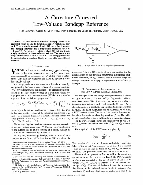
Abstract— A new curvature-corrected bandgap reference is presented which is able to function at supply voltages as low as 1 V, at a supply current of only 100 PA. After trimming this bandgap reference has a temperature coefficient (TC) of +4 ppm/OC. The reference voltage is about 200 mV and it can simply be adjusted to higher reference voltages, The temperature range of this circuit is from O to 125” C. This bandgap reference is realized using a standard bipolar process with base-diffused resistors.
(2)
The capacitor Cml is required to obtain high-frequency stability of the circuit. The transistor Q5 is biased at a current which is twice as large as those of Q1 and Q2 in order to obtain full compensation of the effect of the base currents. The new circuit generating Ivb. as well as the curvaturecorrection current ~~L is shown in Fig. 3. The PTAT currents in Fig. 3 are generated by the circuit shown in Fig. 2. The cttment ~lrb~ = Vbe3/R2 is derived from the base%mitter voltage of Q3. The internal feedback in the circuit ensures that biasing at the indicated current levels is obtained. The transistors Q3 and QZ, which have an emitter–area ratio 1: p,
棒球场布局规则手册说明书

RULE 1 COURT LAYOUT:(a)A court will occupy a level area of at least 50ft (15.24m) in length (in a north-south direction if possible),be at least 10ft (3.05m) in width and consist of two pitcher’s boxes, each 6ft (1.83m) square with a stake inits exact center. The pitcher’s boxes shall be located in such a manner that their front edges are paralleland the stakes are 40ft (12.2m) apart in the middle of the total area.(b) When a number of courts are constructed adjacent to each other as required for tournament play,the stakes of one court shall be at least 10ft (3.05m), 12ft (3.66m) is preferable, from the stakes of adjacentcourts. Foul lines in front of the pitcher’s boxes shall be in a straight line across the entire layout.RULE 2 PITCHING DISTANCE:(a) The pitching distance for men shall be 40ft (12.2m) between the bottoms of the stakes where theyemerge from the ground with a foul line 3ft (91.4cm) in front of each stake.(b) Pitching stakes for women and juniors shall be 30ft (9.14m), with a foul line 3ft (91.4cm) in front of eachstake. When women and juniors play on a court constructed for men, foul lines shall be marked 10ft (3.05m)in front of the men’s foul lines, parallel coming down the sides 6in (15.2cm) to 8in (20.3cm) to give the widthof the pad, with an imaginary stake marked on the ground. A full pad is preferable.(c) Pitching distance for 70 + men shall be any distance behind the women/junior foul line back to themen’s 40ft (12.2m) pad. They shall pitch either 40ft (12.2m) or less than 40ft (12.2m) and establish anaverage at one distance or the other.RULE 3 PITCHER’S BOX:(a) Each pitcher’s box shall be 6ft (1.83m) square with the stake in the exact center and consist of an area ofclay, synthetic substance, dirt or sand into which the players throw their shoes and flanked by two pitchingplatforms or areas from which the players throw their shoes.(b) The clay, dirt, sand or synthetic substance area must be a minimum of 43in (109.2cm) long in thedirection in which the players throw their shoes and 31in (78.7cm) wide. The maximum area is 72in (1.83m)long and 36in (91.4cm) wide. This area must be located in the middle of the pitcher’s box with the stake inits center. This area must be filled to a minimum depth of 4in (10.16cm) and kept in a moist, putty-likecondition if clay is used.(c) The two pitching platforms or areas shall occupy the remaining portions of the pitcher’s box flanking theclay, synthetic substance, dirt or sand area. They must be 6ft (1.83m) long, extending 3ft (91.4cm) in front ofthe stake and be at least 18in (45.7cm). They must be level with each other and with the platforms at theopposite stake. They should be as nearly flush as feasible with the ground outside the pitcher’s box.RULE 4 STAKES:Stakes shall be of cold-rolled steel, mild iron, soft metal, or synthetic material. The top of each stake shallextend not less than 14in (35.56cm) nor more than 15in (38.1cm) above the level of the pitcher’s platformon each side of the stake, with a 3in (7.62cm) incline toward each other.RULE 5 FOUL LINES:(a) Foul lines shall be clearly defined 3ft (91.4cm) in front of each stake across the entire front edge of thepitchers’ box. Foul lines should be used if possible and are required in all National and WorldChampionships.(b) Any shoe pitched while the pitcher’s foot extends on or over the foul line shall be declared foul,and removed from the counting distance.(c) In pitching the shoe, the pitcher shall stand on the pitcher’s platform, at one side or the other ofthe stake.(d) In delivering a shoe, the pitcher must remain behind the foul line until the shoe has left his hand. HOW TO HOLD THE SHOE:Just take the shoe in your hand, feel the weight and grip it in any one of the two ways illustrated.HOW TO PITCH THE SHOE:First you grip the shoe and stand with feet together close to thestake. Next you bring the shoe up at arms length and sight it asyou would a rifle so that the opposite stake appears in the centerof the shoe. (See Fig. 1)Second, you drop the right arm with an easy swinging motion andbring it back past the body, at the same time stepping forward withthe left foot. (See Fig. 2.)Third, you pitch the shoe by bringing the right arm forward and at the same moment step forward withright foot. (See Fig. 3.) The rhythm with which you perform this motion determines the accuracy of yourpitch, provided you have properly gauged the distance.Your forward step must not carry you beyond the box, or more than 3ft (91.4cm) from the stake.and “follow-through”For replacement parts call 1-800-225-8649MA residents call 781-341-5178Made in ChinaFranklin Sports Inc.Stoughton, MA 02072LAYING OUT THE PITCHING COURT:While you can merely drive stakes in the ground 40ft (12.2m) apart and start to pitch, a permanent courtof exact dimensions can be easily laid out and will help you to enjoy the game.The illustration below shows how an Official Court should be laid out. Place sections of twoby four and nail together to make two 6ft (1.83m) squares. The stakes should be driven in the ground inthe center of these boxes inclining slightly toward each other. Fine clay should then be placed around thestakes and tapped down. This clay should be moistened occasionally. The diagram indicates the outerdimensions of the court.PARTS LIST:HorseshoesOFFICIAL HORSESHOE PITCHING RULES AND COURT LAYOUTITEM # 50004Ages 8+。
OSHA现场作业手册说明书
DIRECTIVE NUMBER: CPL 02-00-150 EFFECTIVE DATE: April 22, 2011 SUBJECT: Field Operations Manual (FOM)ABSTRACTPurpose: This instruction cancels and replaces OSHA Instruction CPL 02-00-148,Field Operations Manual (FOM), issued November 9, 2009, whichreplaced the September 26, 1994 Instruction that implemented the FieldInspection Reference Manual (FIRM). The FOM is a revision of OSHA’senforcement policies and procedures manual that provides the field officesa reference document for identifying the responsibilities associated withthe majority of their inspection duties. This Instruction also cancels OSHAInstruction FAP 01-00-003 Federal Agency Safety and Health Programs,May 17, 1996 and Chapter 13 of OSHA Instruction CPL 02-00-045,Revised Field Operations Manual, June 15, 1989.Scope: OSHA-wide.References: Title 29 Code of Federal Regulations §1903.6, Advance Notice ofInspections; 29 Code of Federal Regulations §1903.14, Policy RegardingEmployee Rescue Activities; 29 Code of Federal Regulations §1903.19,Abatement Verification; 29 Code of Federal Regulations §1904.39,Reporting Fatalities and Multiple Hospitalizations to OSHA; and Housingfor Agricultural Workers: Final Rule, Federal Register, March 4, 1980 (45FR 14180).Cancellations: OSHA Instruction CPL 02-00-148, Field Operations Manual, November9, 2009.OSHA Instruction FAP 01-00-003, Federal Agency Safety and HealthPrograms, May 17, 1996.Chapter 13 of OSHA Instruction CPL 02-00-045, Revised FieldOperations Manual, June 15, 1989.State Impact: Notice of Intent and Adoption required. See paragraph VI.Action Offices: National, Regional, and Area OfficesOriginating Office: Directorate of Enforcement Programs Contact: Directorate of Enforcement ProgramsOffice of General Industry Enforcement200 Constitution Avenue, NW, N3 119Washington, DC 20210202-693-1850By and Under the Authority ofDavid Michaels, PhD, MPHAssistant SecretaryExecutive SummaryThis instruction cancels and replaces OSHA Instruction CPL 02-00-148, Field Operations Manual (FOM), issued November 9, 2009. The one remaining part of the prior Field Operations Manual, the chapter on Disclosure, will be added at a later date. This Instruction also cancels OSHA Instruction FAP 01-00-003 Federal Agency Safety and Health Programs, May 17, 1996 and Chapter 13 of OSHA Instruction CPL 02-00-045, Revised Field Operations Manual, June 15, 1989. This Instruction constitutes OSHA’s general enforcement policies and procedures manual for use by the field offices in conducting inspections, issuing citations and proposing penalties.Significant Changes∙A new Table of Contents for the entire FOM is added.∙ A new References section for the entire FOM is added∙ A new Cancellations section for the entire FOM is added.∙Adds a Maritime Industry Sector to Section III of Chapter 10, Industry Sectors.∙Revises sections referring to the Enhanced Enforcement Program (EEP) replacing the information with the Severe Violator Enforcement Program (SVEP).∙Adds Chapter 13, Federal Agency Field Activities.∙Cancels OSHA Instruction FAP 01-00-003, Federal Agency Safety and Health Programs, May 17, 1996.DisclaimerThis manual is intended to provide instruction regarding some of the internal operations of the Occupational Safety and Health Administration (OSHA), and is solely for the benefit of the Government. No duties, rights, or benefits, substantive or procedural, are created or implied by this manual. The contents of this manual are not enforceable by any person or entity against the Department of Labor or the United States. Statements which reflect current Occupational Safety and Health Review Commission or court precedents do not necessarily indicate acquiescence with those precedents.Table of ContentsCHAPTER 1INTRODUCTIONI.PURPOSE. ........................................................................................................... 1-1 II.SCOPE. ................................................................................................................ 1-1 III.REFERENCES .................................................................................................... 1-1 IV.CANCELLATIONS............................................................................................. 1-8 V. ACTION INFORMATION ................................................................................. 1-8A.R ESPONSIBLE O FFICE.......................................................................................................................................... 1-8B.A CTION O FFICES. .................................................................................................................... 1-8C. I NFORMATION O FFICES............................................................................................................ 1-8 VI. STATE IMPACT. ................................................................................................ 1-8 VII.SIGNIFICANT CHANGES. ............................................................................... 1-9 VIII.BACKGROUND. ................................................................................................. 1-9 IX. DEFINITIONS AND TERMINOLOGY. ........................................................ 1-10A.T HE A CT................................................................................................................................................................. 1-10B. C OMPLIANCE S AFETY AND H EALTH O FFICER (CSHO). ...........................................................1-10B.H E/S HE AND H IS/H ERS ..................................................................................................................................... 1-10C.P ROFESSIONAL J UDGMENT............................................................................................................................... 1-10E. W ORKPLACE AND W ORKSITE ......................................................................................................................... 1-10CHAPTER 2PROGRAM PLANNINGI.INTRODUCTION ............................................................................................... 2-1 II.AREA OFFICE RESPONSIBILITIES. .............................................................. 2-1A.P ROVIDING A SSISTANCE TO S MALL E MPLOYERS. ...................................................................................... 2-1B.A REA O FFICE O UTREACH P ROGRAM. ............................................................................................................. 2-1C. R ESPONDING TO R EQUESTS FOR A SSISTANCE. ............................................................................................ 2-2 III. OSHA COOPERATIVE PROGRAMS OVERVIEW. ...................................... 2-2A.V OLUNTARY P ROTECTION P ROGRAM (VPP). ........................................................................... 2-2B.O NSITE C ONSULTATION P ROGRAM. ................................................................................................................ 2-2C.S TRATEGIC P ARTNERSHIPS................................................................................................................................. 2-3D.A LLIANCE P ROGRAM ........................................................................................................................................... 2-3 IV. ENFORCEMENT PROGRAM SCHEDULING. ................................................ 2-4A.G ENERAL ................................................................................................................................................................. 2-4B.I NSPECTION P RIORITY C RITERIA. ..................................................................................................................... 2-4C.E FFECT OF C ONTEST ............................................................................................................................................ 2-5D.E NFORCEMENT E XEMPTIONS AND L IMITATIONS. ....................................................................................... 2-6E.P REEMPTION BY A NOTHER F EDERAL A GENCY ........................................................................................... 2-6F.U NITED S TATES P OSTAL S ERVICE. .................................................................................................................. 2-7G.H OME-B ASED W ORKSITES. ................................................................................................................................ 2-8H.I NSPECTION/I NVESTIGATION T YPES. ............................................................................................................... 2-8 V.UNPROGRAMMED ACTIVITY – HAZARD EVALUATION AND INSPECTION SCHEDULING ............................................................................ 2-9 VI.PROGRAMMED INSPECTIONS. ................................................................... 2-10A.S ITE-S PECIFIC T ARGETING (SST) P ROGRAM. ............................................................................................. 2-10B.S CHEDULING FOR C ONSTRUCTION I NSPECTIONS. ..................................................................................... 2-10C.S CHEDULING FOR M ARITIME I NSPECTIONS. ............................................................................. 2-11D.S PECIAL E MPHASIS P ROGRAMS (SEP S). ................................................................................... 2-12E.N ATIONAL E MPHASIS P ROGRAMS (NEP S) ............................................................................... 2-13F.L OCAL E MPHASIS P ROGRAMS (LEP S) AND R EGIONAL E MPHASIS P ROGRAMS (REP S) ............ 2-13G.O THER S PECIAL P ROGRAMS. ............................................................................................................................ 2-13H.I NSPECTION S CHEDULING AND I NTERFACE WITH C OOPERATIVE P ROGRAM P ARTICIPANTS ....... 2-13CHAPTER 3INSPECTION PROCEDURESI.INSPECTION PREPARATION. .......................................................................... 3-1 II.INSPECTION PLANNING. .................................................................................. 3-1A.R EVIEW OF I NSPECTION H ISTORY .................................................................................................................... 3-1B.R EVIEW OF C OOPERATIVE P ROGRAM P ARTICIPATION .............................................................................. 3-1C.OSHA D ATA I NITIATIVE (ODI) D ATA R EVIEW .......................................................................................... 3-2D.S AFETY AND H EALTH I SSUES R ELATING TO CSHO S.................................................................. 3-2E.A DVANCE N OTICE. ................................................................................................................................................ 3-3F.P RE-I NSPECTION C OMPULSORY P ROCESS ...................................................................................................... 3-5G.P ERSONAL S ECURITY C LEARANCE. ................................................................................................................. 3-5H.E XPERT A SSISTANCE. ........................................................................................................................................... 3-5 III. INSPECTION SCOPE. ......................................................................................... 3-6A.C OMPREHENSIVE ................................................................................................................................................... 3-6B.P ARTIAL. ................................................................................................................................................................... 3-6 IV. CONDUCT OF INSPECTION .............................................................................. 3-6A.T IME OF I NSPECTION............................................................................................................................................. 3-6B.P RESENTING C REDENTIALS. ............................................................................................................................... 3-6C.R EFUSAL TO P ERMIT I NSPECTION AND I NTERFERENCE ............................................................................. 3-7D.E MPLOYEE P ARTICIPATION. ............................................................................................................................... 3-9E.R ELEASE FOR E NTRY ............................................................................................................................................ 3-9F.B ANKRUPT OR O UT OF B USINESS. .................................................................................................................... 3-9G.E MPLOYEE R ESPONSIBILITIES. ................................................................................................. 3-10H.S TRIKE OR L ABOR D ISPUTE ............................................................................................................................. 3-10I. V ARIANCES. .......................................................................................................................................................... 3-11 V. OPENING CONFERENCE. ................................................................................ 3-11A.G ENERAL ................................................................................................................................................................ 3-11B.R EVIEW OF A PPROPRIATION A CT E XEMPTIONS AND L IMITATION. ..................................................... 3-13C.R EVIEW S CREENING FOR P ROCESS S AFETY M ANAGEMENT (PSM) C OVERAGE............................. 3-13D.R EVIEW OF V OLUNTARY C OMPLIANCE P ROGRAMS. ................................................................................ 3-14E.D ISRUPTIVE C ONDUCT. ...................................................................................................................................... 3-15F.C LASSIFIED A REAS ............................................................................................................................................. 3-16VI. REVIEW OF RECORDS. ................................................................................... 3-16A.I NJURY AND I LLNESS R ECORDS...................................................................................................................... 3-16B.R ECORDING C RITERIA. ...................................................................................................................................... 3-18C. R ECORDKEEPING D EFICIENCIES. .................................................................................................................. 3-18 VII. WALKAROUND INSPECTION. ....................................................................... 3-19A.W ALKAROUND R EPRESENTATIVES ............................................................................................................... 3-19B.E VALUATION OF S AFETY AND H EALTH M ANAGEMENT S YSTEM. ....................................................... 3-20C.R ECORD A LL F ACTS P ERTINENT TO A V IOLATION. ................................................................................. 3-20D.T ESTIFYING IN H EARINGS ................................................................................................................................ 3-21E.T RADE S ECRETS. ................................................................................................................................................. 3-21F.C OLLECTING S AMPLES. ..................................................................................................................................... 3-22G.P HOTOGRAPHS AND V IDEOTAPES.................................................................................................................. 3-22H.V IOLATIONS OF O THER L AWS. ....................................................................................................................... 3-23I.I NTERVIEWS OF N ON-M ANAGERIAL E MPLOYEES .................................................................................... 3-23J.M ULTI-E MPLOYER W ORKSITES ..................................................................................................................... 3-27 K.A DMINISTRATIVE S UBPOENA.......................................................................................................................... 3-27 L.E MPLOYER A BATEMENT A SSISTANCE. ........................................................................................................ 3-27 VIII. CLOSING CONFERENCE. .............................................................................. 3-28A.P ARTICIPANTS. ..................................................................................................................................................... 3-28B.D ISCUSSION I TEMS. ............................................................................................................................................ 3-28C.A DVICE TO A TTENDEES .................................................................................................................................... 3-29D.P ENALTIES............................................................................................................................................................. 3-30E.F EASIBLE A DMINISTRATIVE, W ORK P RACTICE AND E NGINEERING C ONTROLS. ............................ 3-30F.R EDUCING E MPLOYEE E XPOSURE. ................................................................................................................ 3-32G.A BATEMENT V ERIFICATION. ........................................................................................................................... 3-32H.E MPLOYEE D ISCRIMINATION .......................................................................................................................... 3-33 IX. SPECIAL INSPECTION PROCEDURES. ...................................................... 3-33A.F OLLOW-UP AND M ONITORING I NSPECTIONS............................................................................................ 3-33B.C ONSTRUCTION I NSPECTIONS ......................................................................................................................... 3-34C. F EDERAL A GENCY I NSPECTIONS. ................................................................................................................. 3-35CHAPTER 4VIOLATIONSI. BASIS OF VIOLATIONS ..................................................................................... 4-1A.S TANDARDS AND R EGULATIONS. .................................................................................................................... 4-1B.E MPLOYEE E XPOSURE. ........................................................................................................................................ 4-3C.R EGULATORY R EQUIREMENTS. ........................................................................................................................ 4-6D.H AZARD C OMMUNICATION. .............................................................................................................................. 4-6E. E MPLOYER/E MPLOYEE R ESPONSIBILITIES ................................................................................................... 4-6 II. SERIOUS VIOLATIONS. .................................................................................... 4-8A.S ECTION 17(K). ......................................................................................................................... 4-8B.E STABLISHING S ERIOUS V IOLATIONS ............................................................................................................ 4-8C. F OUR S TEPS TO BE D OCUMENTED. ................................................................................................................... 4-8 III. GENERAL DUTY REQUIREMENTS ............................................................. 4-14A.E VALUATION OF G ENERAL D UTY R EQUIREMENTS ................................................................................. 4-14B.E LEMENTS OF A G ENERAL D UTY R EQUIREMENT V IOLATION.............................................................. 4-14C. U SE OF THE G ENERAL D UTY C LAUSE ........................................................................................................ 4-23D.L IMITATIONS OF U SE OF THE G ENERAL D UTY C LAUSE. ..............................................................E.C LASSIFICATION OF V IOLATIONS C ITED U NDER THE G ENERAL D UTY C LAUSE. ..................F. P ROCEDURES FOR I MPLEMENTATION OF S ECTION 5(A)(1) E NFORCEMENT ............................ 4-25 4-27 4-27IV.OTHER-THAN-SERIOUS VIOLATIONS ............................................... 4-28 V.WILLFUL VIOLATIONS. ......................................................................... 4-28A.I NTENTIONAL D ISREGARD V IOLATIONS. ..........................................................................................4-28B.P LAIN I NDIFFERENCE V IOLATIONS. ...................................................................................................4-29 VI. CRIMINAL/WILLFUL VIOLATIONS. ................................................... 4-30A.A REA D IRECTOR C OORDINATION ....................................................................................................... 4-31B.C RITERIA FOR I NVESTIGATING P OSSIBLE C RIMINAL/W ILLFUL V IOLATIONS ........................ 4-31C. W ILLFUL V IOLATIONS R ELATED TO A F ATALITY .......................................................................... 4-32 VII. REPEATED VIOLATIONS. ...................................................................... 4-32A.F EDERAL AND S TATE P LAN V IOLATIONS. ........................................................................................4-32B.I DENTICAL S TANDARDS. .......................................................................................................................4-32C.D IFFERENT S TANDARDS. .......................................................................................................................4-33D.O BTAINING I NSPECTION H ISTORY. .....................................................................................................4-33E.T IME L IMITATIONS..................................................................................................................................4-34F.R EPEATED V. F AILURE TO A BATE....................................................................................................... 4-34G. A REA D IRECTOR R ESPONSIBILITIES. .............................................................................. 4-35 VIII. DE MINIMIS CONDITIONS. ................................................................... 4-36A.C RITERIA ................................................................................................................................................... 4-36B.P ROFESSIONAL J UDGMENT. ..................................................................................................................4-37C. A REA D IRECTOR R ESPONSIBILITIES. .............................................................................. 4-37 IX. CITING IN THE ALTERNATIVE ............................................................ 4-37 X. COMBINING AND GROUPING VIOLATIONS. ................................... 4-37A.C OMBINING. ..............................................................................................................................................4-37B.G ROUPING. ................................................................................................................................................4-38C. W HEN N OT TO G ROUP OR C OMBINE. ................................................................................................4-38 XI. HEALTH STANDARD VIOLATIONS ....................................................... 4-39A.C ITATION OF V ENTILATION S TANDARDS ......................................................................................... 4-39B.V IOLATIONS OF THE N OISE S TANDARD. ...........................................................................................4-40 XII. VIOLATIONS OF THE RESPIRATORY PROTECTION STANDARD(§1910.134). ....................................................................................................... XIII. VIOLATIONS OF AIR CONTAMINANT STANDARDS (§1910.1000) ... 4-43 4-43A.R EQUIREMENTS UNDER THE STANDARD: .................................................................................................. 4-43B.C LASSIFICATION OF V IOLATIONS OF A IR C ONTAMINANT S TANDARDS. ......................................... 4-43 XIV. CITING IMPROPER PERSONAL HYGIENE PRACTICES. ................... 4-45A.I NGESTION H AZARDS. .................................................................................................................................... 4-45B.A BSORPTION H AZARDS. ................................................................................................................................ 4-46C.W IPE S AMPLING. ............................................................................................................................................. 4-46D.C ITATION P OLICY ............................................................................................................................................ 4-46 XV. BIOLOGICAL MONITORING. ...................................................................... 4-47CHAPTER 5CASE FILE PREPARATION AND DOCUMENTATIONI.INTRODUCTION ............................................................................................... 5-1 II.INSPECTION CONDUCTED, CITATIONS BEING ISSUED. .................... 5-1A.OSHA-1 ................................................................................................................................... 5-1B.OSHA-1A. ............................................................................................................................... 5-1C. OSHA-1B. ................................................................................................................................ 5-2 III.INSPECTION CONDUCTED BUT NO CITATIONS ISSUED .................... 5-5 IV.NO INSPECTION ............................................................................................... 5-5 V. HEALTH INSPECTIONS. ................................................................................. 5-6A.D OCUMENT P OTENTIAL E XPOSURE. ............................................................................................................... 5-6B.E MPLOYER’S O CCUPATIONAL S AFETY AND H EALTH S YSTEM. ............................................................. 5-6 VI. AFFIRMATIVE DEFENSES............................................................................. 5-8A.B URDEN OF P ROOF. .............................................................................................................................................. 5-8B.E XPLANATIONS. ..................................................................................................................................................... 5-8 VII. INTERVIEW STATEMENTS. ........................................................................ 5-10A.G ENERALLY. ......................................................................................................................................................... 5-10B.CSHO S SHALL OBTAIN WRITTEN STATEMENTS WHEN: .......................................................................... 5-10C.L ANGUAGE AND W ORDING OF S TATEMENT. ............................................................................................. 5-11D.R EFUSAL TO S IGN S TATEMENT ...................................................................................................................... 5-11E.V IDEO AND A UDIOTAPED S TATEMENTS. ..................................................................................................... 5-11F.A DMINISTRATIVE D EPOSITIONS. .............................................................................................5-11 VIII. PAPERWORK AND WRITTEN PROGRAM REQUIREMENTS. .......... 5-12 IX.GUIDELINES FOR CASE FILE DOCUMENTATION FOR USE WITH VIDEOTAPES AND AUDIOTAPES .............................................................. 5-12 X.CASE FILE ACTIVITY DIARY SHEET. ..................................................... 5-12 XI. CITATIONS. ..................................................................................................... 5-12A.S TATUTE OF L IMITATIONS. .............................................................................................................................. 5-13B.I SSUING C ITATIONS. ........................................................................................................................................... 5-13C.A MENDING/W ITHDRAWING C ITATIONS AND N OTIFICATION OF P ENALTIES. .................................. 5-13D.P ROCEDURES FOR A MENDING OR W ITHDRAWING C ITATIONS ............................................................ 5-14 XII. INSPECTION RECORDS. ............................................................................... 5-15A.G ENERALLY. ......................................................................................................................................................... 5-15B.R ELEASE OF I NSPECTION I NFORMATION ..................................................................................................... 5-15C. C LASSIFIED AND T RADE S ECRET I NFORMATION ...................................................................................... 5-16。
Nanosim_2004_Jan仿真教程
2004.January
Nanosim Training Course
Page 5
Logic vs. SPICE vs. “Fast SPICE” (1/2)
Logic Simulator (VCS):
¾ High performance, high capacity ¾ Digital only ¾ Time based, unit delay
macro models, Verilog-A Back-end full chip verification (SoC) Simulation with mixed netlist types
2004.January
Nanosim Training Course
Page 8
SPICE format for most sources accepted Verilog gate-level netlists accepted (with subckt
12 LPE PVS (CalibrePEX)
13
Simulation PVS
(NanoSim)
Physical Optimization
(Optional)
6
7
Timing Optimization
Physical Compiler
Tape
14
Out
Mixed-Signal Design Flow
2004.January
Nanosim Training Course
Page 6
Logic vs. SPICE vs. “Fast SPICE” (2/2)
“Fast SPICE” (NanoSim):
¾ Best of both worlds ¾ Gate level capacity, spice-like accuracy
光子晶体导波基本原理说明书
More informationFundamentals of Photonic Crystal GuidingIf you’re looking to understand photonic crystals,this systematic,rigorous,and peda-gogical introduction is a must.Here you’llfind intuitive analytical and semi-analyticalmodels applied to complex and practically relevant photonic crystal structures.Y ou willalso be shown how to use various analytical methods borrowed from quantum mechanics,such as perturbation theory,asymptotic analysis,and group theory,to investigate manyof the limiting properties of photonic crystals,which are otherwise difficult to rationalizeusing only numerical simulations.An introductory review of nonlinear guiding in photonic lattices is also presented,as are the fabrication and application of photonic crystals.In addition,end-of-chapterexercise problems with detailed analytical and numerical solutions allow you to monitoryour understanding of the material presented.This accessible text is ideal for researchersand graduate students studying photonic crystals in departments of electrical engineering,physics,applied physics,and mathematics.Maksim Skorobogatiy is Professor and Canada Research Chair in Photonic Crystals atthe Department of Engineering Physics in´Ecole Polytechnique de Montr´e al,Canada.In2005he was awarded a fellowship from the Japanese Society for Promotion of Science,and he is a member of the Optical Society of America.Jianke Yang is Professor of Applied Mathematics at the University of Vermont,USA.Heis a member of the Optical Society of America and the Society of Industrial and AppliedMathematics.Fundamentals of Photonic Crystal GuidingMAKSIM SKOROBOGATIY 1JIANKE YANG 2´Ecole Polytechnique de Montr ´e al,Canada 1University of Vermont,USA2More informationMore informationcambridge university pressCambridge,New Y ork,Melbourne,Madrid,Cape Town,Singapore,S˜a o Paulo,DelhiCambridge University PressThe Edinburgh Building,Cambridge CB28RU,UKPublished in the United States of America by Cambridge University Press,New Y orkInformation on this title:/9780521513289C Cambridge University Press2009This publication is in copyright.Subject to statutory exceptionand to the provisions of relevant collective licensing agreements,no reproduction of any part may take place withoutthe written permission of Cambridge University Press.First published2009Printed in the United Kingdom at the University Press,CambridgeA catalog record for this publication is available from the British LibraryLibrary of Congress Cataloging in Publication dataSkorobogatiy,Maksim,1974–Fundamentals of photonic crystal guiding/by Maksim Skorobogatiy and Jianke Y ang.p.cm.Includes index.ISBN978-0-521-51328-91.Photonic crystals.I.Y ang,Jianke.II.Title.QD924.S562008621.36–dc222008033576ISBN978-0-521-51328-9hardbackCambridge University Press has no responsibility for the persistence oraccuracy of URLs for external or third-party internet websites referred toin this publication,and does not guarantee that any content on suchwebsites is,or will remain,accurate or appropriate.More informationM.Skorobogatiy dedicates this book to his family.He thanks his parentsAlexander and Tetyana for never-ceasing support,encouragement,andparticipation in all his endeavors.He also thanks his wife Olga,his children,Alexander junior and Anastasia,andhis parents for their unconditional love.J.Yang dedicates this book to his family.More informationContentsPreface page xiAcknowledgements xii1Introduction11.1Fabrication of photonic crystals21.2Application of photonic crystals41.2.1Photonic crystals as low-loss mirrors:photonicbandgap effects41.2.2Photonic crystals for out-of-bandgap operation10References112Hamiltonian formulation of Maxwell’s equations(frequency consideration)142.1Plane-wave solution for uniform dielectrics162.2Methods of quantum mechanics in electromagnetism182.2.1Orthogonality of eigenstates192.2.2Variational principle202.2.3Equivalence between the eigenstates of twocommuting Hamiltonians222.2.4Eigenstates of the operators of continuous anddiscrete translations and rotations232.3Properties of the harmonic modes of Maxwell’s equations302.3.1Orthogonality of electromagnetic modes322.3.2Eigenvalues and the variational principle322.3.3Absence of the fundamental length scale in Maxwell’sequations342.4Symmetries of electromagnetic eigenmodes352.4.1Time-reversal symmetry352.4.2Definition of the operators of translation and rotation352.4.3Continuous translational and rotational symmetries382.4.4Band diagrams432.4.5Discrete translational and rotational symmetries44More informationviii Contents2.4.6Discrete translational symmetry and discreterotational symmetry522.4.7Inversion symmetry,mirror symmetry,and other symmetries532.5Problems553One-dimensional photonic crystals–multilayer stacks593.1Transfer matrix technique593.1.1Multilayer stack,TE polarization593.1.2Multilayer stack,TM polarization613.1.3Boundary conditions623.2Reflection from afinite multilayer(dielectric mirror)633.3Reflection from a semi-infinite multilayer(dielectricphotonic crystal mirror)643.3.1Omnidirectional reflectors I683.4Guiding in afinite multilayer(planar dielectric waveguide)693.5Guiding in the interior of an infinitely periodic multilayer703.5.1Omnidirectional reflectors II803.6Defect states in a perturbed periodic multilayer:planarphotonic crystal waveguides823.7Problems864Bandgap guidance in planar photonic crystal waveguides934.1Design considerations of waveguides with infinitelyperiodic reflectors934.2Fundamental TE mode of a waveguide with infinitelyperiodic reflector964.3Infinitely periodic reflectors,field distribution in TM modes984.3.1Case of the core dielectric constantεc<εhεl/(εh+εl)984.3.2Case of the core dielectric constantεl≥εc>εhεl/(εh+εl)1014.4Perturbation theory for Maxwell’s equations,frequencyformulation1034.4.1Accounting for the absorption losses of the waveguidematerials:calculation of the modal lifetime and decay length1044.5Perturbative calculation of the modal radiation loss in aphotonic bandgap waveguide with afinite reflector1064.5.1Physical approach1064.5.2Mathematical approach1085Hamiltonian formulation of Maxwell’s equations for waveguides(propagation-constant consideration)1105.1Eigenstates of a waveguide in Hamiltonian formulation1105.1.1Orthogonality relation between the modes of a waveguide madeof lossless dielectrics111More informationContents ix5.1.2Expressions for the modal phase velocity1145.1.3Expressions for the modal group velocity1145.1.4Orthogonality relation between the modes of a waveguide madeof lossy dielectrics1155.2Perturbation theory for uniform variations in a waveguide dielectric profile1165.2.1Perturbation theory for the nondegenerate modes:example ofmaterial absorption1185.2.2Perturbation theory for the degenerate modes coupled byperturbation:example of polarization-mode dispersion1205.2.3Perturbations that change the positions of dielectric interfaces1235.3Problems126References127 6Two-dimensional photonic crystals1296.1T wo-dimensional photonic crystals with diminishingly smallindex contrast1296.2Plane-wave expansion method1326.2.1Calculation of the modal group velocity1346.2.2Plane-wave method in2D1346.2.3Calculation of the group velocity in the case of2Dphotonic crystals1356.2.4Perturbative formulation for the photonic crystallattices with small refractive index contrast1386.2.5Photonic crystal lattices with high-refractive-index contrast1426.3Comparison between various projected band diagrams1426.4Dispersion relation at a band edge,density of states andVan Hove singularities1446.5Refraction from photonic crystals1476.6Defects in a2D photonic crystal lattice1486.6.1Line defects1486.6.2Point defects1586.7Problems167References171 7Quasi-2D photonic crystals1727.1Photonic crystalfibers1727.1.1Plane-wave expansion method1727.1.2Band diagram of modes of a photonic crystalfiber1767.2Optically induced photonic lattices1777.2.1Light propagation in low-index-contrast periodicphotonic lattices1787.2.2Defect modes in2D photonic lattices with localized defects1817.2.3Bandgap structure and diffraction relation for the modes of auniform lattice182More informationx Contents7.2.4Bifurcations of the defect modes from Bloch band edges forlocalized weak defects1857.2.5Dependence of the defect modes on the strength oflocalized defects1887.2.6Defect modes in2D photonic lattices with nonlocalized defects1927.3Photonic-crystal slabs1957.3.1Geometry of a photonic-crystal slab1957.3.2Eigenmodes of a photonic-crystal slab1977.3.3Analogy between the modes of a photonic-crystal slab and themodes of a corresponding2D photonic crystal2007.3.4Modes of a photonic-crystal slab waveguide2047.4Problems207References208 8Nonlinear effects and gap–soliton formation in periodic media2108.1Solitons bifurcated from Bloch bands in1D periodic media2118.1.1Bloch bands and bandgaps2118.1.2Envelope equations of Bloch modes2128.1.3Locations of envelope solitons2158.1.4Soliton families bifurcated from band edges2168.2Solitons bifurcated from Bloch bands in2D periodic media2188.2.1T wo-dimensional Bloch bands and bandgaps of linearperiodic systems2198.2.2Envelope equations of2D Bloch modes2208.2.3Families of solitons bifurcated from2D band edges2238.3Soliton families not bifurcated from Bloch bands2268.4Problems227References228Problem solutions230Chapter2230Chapter3236Chapter5244Chapter6246Chapter7257Chapter8260 Index263More informationPrefaceThefield of photonic crystals(aka periodic photonic structures)is experiencing anunprecedented growth due to the dramatic ways in which such structures can control,modify,and harvest theflow of light.The idea of writing this book came to M.Skorobogatiy when he was developingan introductory course on photonic crystals at the Ecole Polytechnique de Montr´e al/University of Montr´e al.Thefield of photonic crystals,being heavily dependent onnumerical simulations,is somewhat challenging to introduce without sacrificing thequalitative understanding of the underlying physics.On the other hand,exactly solvablemodels,where the relation between physics and quantitative results is most transpar-ent,only exist for photonic crystals of trivial geometries.The challenge,therefore,wasto develop a presentational approach that would maximally use intuitive analytical andsemi-analytical models,while applying them to complex and practically relevant pho-tonic crystal structures.We would like to note that the main purpose of this book is not to present the latestadvancements in thefield of photonic crystals,but rather to give a systematic,logical,andpedagogical introduction to this vibrantfield.The text is largely aimed at students andresearchers who want to acquire a rigorous,while intuitive,mathematical introductioninto the subject of guided modes in photonic crystals and photonic crystal waveguides.The text,therefore,favors analysis of analytically or semi-analytically solvable problemsover pure numerical modeling.We believe that this is a more didactical approach whentrying to introduce a novice into a newfield.To further stimulate understanding of thebook content,we suggest many exercise problems of physical relevance that can besolved analytically.In the course of the book we extensively use the analogy between the Hamiltonian for-mulation of Maxwell’s equations and the Hamiltonian formulation of quantum mechan-ics.We present both frequency and propagation-constant based Hamiltonian formula-tions of Maxwell’s equations.The latter is particularly useful for analyzing photoniccrystal-based linear and nonlinear waveguides andfibers.This approach allows us touse a well-developed machinery of quantum mechanical semi-analytical methods,suchas perturbation theory,asymptotic analysis,and group theory,to investigate many ofthe limiting properties of photonic crystals,which are otherwise difficult to investigatebased only on numerical simulations.M.Skorobogatiy has contributed Chapters2,3,4,5,and6of this book,and J.Y anghas contributed Chapter8.Chapters1and7were co-authored by both authors.More informationAcknowledgementsM.Skorobogatiy would like to thank his graduate and postgraduate program mentors,Professor J.D.Joannopoulos and Professor Y.Fink from MIT,for introducing him intothefield of photonic crystals.He is grateful to Professor M.Koshiba and ProfessorK.Saitoh for hosting him at Hokkaido University in2005and for having many excitingdiscussions in the area of photonic crystalfibers.M.Skorobogatiy acknowledges theCanada Research Chair program for making this book possible by reducing his teachingload.J.Y ang thanks the funding support of the US Air Force Office of Scientific Research,which made many results of this book possible.He also thanks the Zhou Pei-Yuan Centerfor Applied Mathematics at Tsinghua University(China)for hospitality during his visit,where portions of this book were written.Both authors are grateful to their graduate andpostgraduate students for their comments and help,while this book was in preparation.Especially,J.Y ang likes to thank Dr.Jiandong Wang,whose help was essential for hisbook writing.。
67255_AD_AD680AN
CONNECTION DIAGRAMSTP*+V IN TEMP GNDTP*TP*V OUT NCNC = NO CONNECTTP DENOTES FACTORY TEST POINT.NO CONNECTIONS SHOULD BE MADE TO THESE PINS.*REV.CInformation furnished by Analog Devices is believed to be accurate and reliable. However, no responsibility is assumed by Analog Devices for its use, nor for any infringements of patents or other rights of third parties which may result from its use. No license is granted by implication or otherwise under any patent or patent rights of Analog Devices.aLow Power, Low Cost2.5 V ReferenceAD680*FEATURESLow Quiescent Current: 250 A max Laser Trimmed to High Accuracy:2.5 V ؎5 mV max (AN, AR Grade)Trimmed Temperature Coefficient:20 ppm/؇C max (AN, AR Grade)Low Noise: 8 V p-p from 0.1 Hz to 10 Hz 250 nV/√Hz WidebandTemperature Output Pin (N, R Packages)Available in Three Package Styles:8-Pin Plastic DIP, 8-Pin SOIC and 3-Pin TO-92One Technology Way, P.O. Box 9106, Norwood, MA 02062-9106, U.S.A.Tel: 617/329-4700Fax: 617/326-8703PRODUCT DESCRIPTIONThe AD680 is a bandgap voltage reference which provides a fixed 2.5 V output from inputs between 4.5 V and 36 V. The architecture of the AD680 enables the reference to be operated at a very low quiescent current while still realizing excellent dc characteristics and noise performance. Trimming of the high stability thin-film resistors is performed for initial accuracy and temperature coefficient, resulting in low errors over temperature.The precision dc characteristics of the AD680 make it ideal for use as a reference for D/A converters which require an external precision reference. The device is also ideal for A/D converters and, in general, can offer better performance than the standard on-chip references.Based upon the low quiescent current of the AD680, which rivals that of many incomplete two-terminal references, the AD680 is recommended for low power applications such as hand-held battery equipment.A temperature output pin is provided on the 8-pin package ver-sions of the AD680. The temperature output pin provides an output voltage that varies linearly with temperature and allows the AD680 to be configured as a temperature transducer while providing a stable 2.5 V output.The AD680 is available in five grades. The AD680AN is speci-fied for operation from –40°C to +85°C, while the AD680JN is specified for 0°C to +70°C operation. Both the AD680AN and AD680JN are available in 8-pin plastic DIP packages. The AD680AR is specified for operation from –40°C to +85°C,while the AD680JR is specified for 0°C to +70°C operation.Both are available in an 8-pin Small Outline IC (SOIC) pack-age. The AD680JT is specified for 0°C to +70°C operation and is available in a 3-pin TO-92 package.*Protected by U.S. Patent Nos. 4,902,959; 4,250,445 and 4,857,862.PRODUCT HIGHLIGHTS1. The AD680 bandgap reference operates on a very low quies-cent current which rivals that of many two-terminal refer-ences. This makes the complete, higher accuracy AD680ideal for use in power sensitive applications.2. Laser trimming of both initial accuracy and temperaturecoefficients results in low errors over temperature without the use of external components. The AD680AN and AD680AR have a maximum variation of 6.25 mV between –40°C and +85°C.3. The AD680 noise is low, typically 8 µV p-p from 0.1 Hz to 10 Hz. Spectral density is also low, typically 250 nV/√Hz .4. The temperature output pin on the 8-pin package versions enables the AD680 to be configured as a temperature trans-ducer.5. Plastic DIP packaging provides machine insertability, while SOIC packaging provides surface mount capability. TO-92packaging offers a cost effective alternative to two-terminal references, offering a complete solution in the same package in which two-terminal references are usually found.AD680–SPECIFICATIONSAD680AN/ARAD680JN/JR AD680JT ModelMin Typ MaxMin Typ Max Min Typ Max Units OUTPUT VOLTAGE 2.4952.5052.4902.510 2.4902.510V OUTPUT VOLTAGE DRIFT 10°C to +70°C 1010251030ppm/°C–40°C to +85°C 202525LINE REGULATION 4.5 V ≤ +V IN ≤ 15 V 40**µV/V(@ T MIN to T MAX )40**15 V ≤ +V IN ≤ 36 V 40** (@ T MIN to T MAX )40**LOAD REGULATION 0 < I OUT < 10 mA 80100****µV/mA (@ T MIN to T MAX )80100****QUIESCENT CURRENT 195250****µA (@ T MIN to T MAX )280**POWER DISSIPATION 1 1.25****mW OUTPUT NOISE 0.1 Hz to 10 Hz810****mV p-p Spectral Density, 100 Hz 250**nV/√Hz CAPACITIVE LOAD 50**nFLONG TERM STABILITY 25**ppm/1000 hrSHORT CIRCUIT CURRENT TO GROUND 2550****mA TEMPERATURE PINVoltage Output @ +25°C 540596660***mV Temperature Sensitivity 2*mV/°C Output Current –5+5**µA Output Resistance 12*k ΩTEMPERATURE RANGE Specified Performance –40+850+700+70°COperating Performance 2–40+85–40+85–40+85NOTES 1Maximum output voltage drift is guaranteed for all packages.2The operating temperature range is defined as the temperature extremes at which the device will still function. Parts may deviate from their specified performance outside their specified temperature range.*Same as AD680AN/AR specification.Specifications subject to change without notice.Specifications in boldface are tested on all production units at final eleetrical test. Results from those tests are used to calculate out going quality levels. All min and max specifications are guaranteed.(T A = +25؇C, V IN = +5 V, unless otherwise noted)REV. C–2–AD680REV. C –3–THEORY OF OPERATIONBandgap references are the high performance solution for low supply voltage operation. A typical precision bandgap will con-sist of a reference core and buffer amplifier. Based on a new,patented bandgap reference design (Figure 2), the AD680merges the amplifier and the core bandgap function to produce a compact, complete precision reference. Central to the device is a high gain amplifier with an intentionally large Proportional To Absolute Temperature (PTAT) input offset. This offset is controlled by the area ratio of the amplifier input pair, Q1 and Q2, and is developed across resistor R1. Transistor Q12’s base emitter voltage has a Complementary To Absolute Temperature (CTAT) characteristic. Resistor R2 and the parallel combina-tion of R3 and R4 “multiply” the PTAT voltage across R1.Trimming resistors R3 and R4 to the proper ratio produces a temperature invariant 2.5 V at the output. The result is an accurate, stable output voltage accomplished with a minimum number of components.R5OUT+V INFigure 2.AD680 Schematic DiagramAn additional feature with this approach is the ability to mini-mize the noise while maintaining very low overall power dissipation for the entire circuit. Frequently it is difficult to independently control the dominant noise sources for bandgap references: bandgap transistor noise and resistor thermal noise.By properly choosing the operating currents of Q1 and Q2 and separately sizing R1, low wideband noise is realized while main-taining 1 mW typical power dissipation.ABSOLUTE MAXIMUM RATINGS*V IN to Ground . . . . . . . . . . . . . . . . . . . . . . . . . . . . . . . . . .36 V Power Dissipation (25°C) . . . . . . . . . . . . . . . . . . . . . .500 mW Storage Temperature . . . . . . . . . . . . . . . . . . .–65°C to +125°C Lead Temperature (Soldering, 10 sec) . . . . . . . . . . . . . .300°C Package Thermal ResistanceθJA (All Packages) . . . . . . . . . . . . . . . . . . . . . . . .120°C/W Output Protection: Output safe for indefinite short to ground and momentary short to V IN .*Stresses above those listed under “Absolute Maximum Ratings” may cause permanent damage to the device. This is a stress rating only and functional operation of the device at these or any other conditions above those indicated in the operational sections of this specification is not implied. Exposure to absolutemaximum rating conditions for extended periods may affect device reliability.8-Pin Plastic DIPand8-Pin SOIC PackagesTP*+V IN TEMP GNDTP*TP*V OUT NCNC = NO CONNECTTP DENOTES FACTORY TEST POINT.NO CONNECTIONS SHOULD BE MADE TO THESE PINS.*TO-92 PackageFigure 1. Connection DiagramsORDERING GUIDEInitial Temperature Error Coeff.Temperature Package Package Model mV ppm/°C Range Description Option*AD680JN 10250°C to +70°C Plastic N-8AD680JR 10250°C to +70°C SOIC SO-8AD680JT 10300°C to +70°C TO-92TO-92AD680AN 520–40°C to +85°C Plastic N-8AD680AR520–40°C to +85°CSOICSO-8*N = Plastic DIP Package; SO = SOIC Package; T = TO-92 Package.AD680REV. C–4–APPLYING THE AD680The AD680 is simple to use in virtually all precision reference applications. When power is applied to +V IN and the GND pin is tied to ground, V OUT provides a +2.5 V output. The AD680typically requires less than 250 µA of current when operating from a supply of +4.5 V to +36 V.To operate the AD680, the +V IN pin must be bypassed to the GND pin with a 0.1 µF capacitor tied as close to the AD680 as possible. Although the ground current for the AD680 is small (typically 195 µA), a direct connection should be made between the AD680 GND pin and the system ground plane.Reference outputs are frequently required to handle fast tran-sients caused by input switching networks, as are commonly found in ADCs and measurement instrumentation equipment.Many of the dynamic problems associated with this situation can be minimized with a few simple techniques. Using a series resistor between the reference output and the load will tend to “decouple” the reference output from the transient source. Or a relatively large capacitor connected from the reference output to ground can serve as a charge storage element to absorb and de-liver charge as is required by the dynamic load. A 50 nF capaci-tor is recommended for the AD680 in this case; this is large enough to store the required charge, but small enough so as not to disrupt the stability of the reference.The 8-pin plastic DIP and SOIC packaged versions of the AD680 also provide a temperature output pin. The voltage on this pin is nominally 596 mV at 25°C. This pin will provide an output linearly proportional to temperature with a characteristic of 2 mV/°C.NOISE PERFORMANCEThe noise generated by the AD680 is typically less than 8 µV p-p over the 0.1 Hz to 10 Hz band. Figure 3 shows the 0.1 Hz to 10 Hz noise of a typical AD680. The noise measurement is made with a bandpass filter made of a 1-pole high-pass filter with a corner frequency at 0.1 Hz and a 2-pole low-pass filter with a corner frequency at 12.6 Hz to create a filter with a9.922 Hz bandwidth.Figure 3.0.1 Hz to 10 Hz NoiseNoise in a 300 kHz bandwidth is approximately 800 µV p-p.Figure 4 shows the broadband noise of a typical AD680.Figure 4.Broadband Noise at 300 kHzTURN-ON TIMEUpon application of power (cold start), the time required for the output voltage to reach its final value within a specified error band is defined as the turn-on settling time. Two components normally associated with this are: the time for the active circuits to settle, and the time for the thermal gradients on the chip to stabilize. Figure 5 shows the turn-on settling time of the AD680to be about 20 µs to 0.025% of its final value.Figure 5.Turn-On Settling TimeThe AD680 thermal settling characteristic benefits from itscompact design. Once initial turn-on is achieved, the output lin-early approaches its final value; the output is typically within 0.01% of its final value after 25 ms.DYNAMIC PERFORMANCEThe output stage of the ampliflier is designed to provide the AD680 with static and dynamic load regulation superior to lesscomplete references.AD680REV. C –5–Figure 6 displays the characteristics of the AD680 output ampli-fier driving a 0 mA to 10 mA load. Longer settling times will re-sult if the reference is forced to sink any transient current.In some applications, a varying load may be both resistive and capacitive in nature, or the load may be connected to the AD680 by a long capacitive cable.+VOUT0.1 µFFigure 6a.Transient Load Test CircuitFigure rge-Scale Transient ResponseFigure 6c.Fine Scale Settling for Transient LoadFigure 7 displays the output amplifier characteristics driving a 1000 pF, 0 mA to 10 mA load.OUT+V 0.1 µFFigure 7a.Capacitive Load Transient Response Test CircuitFigure 7b.Output Response with Capacitive LoadLOAD REGULATIONFigure 8 shows the load regulation characteristics of the AD680.Figure 8.Typical Load Regulation CharacteristicsAD680REV. C–6–TEMPERATURE PERFORMANCEThe AD680 is designed for reference applications where tem-perature performancc is important. Extensivc temperature test-ing and characterization ensures that the device’s performance is maintained over the specified temperature range.Some confusion exists in thc area of defining and specifying ref-erence voltage error over temperature. Historically, references have been characterized using a maximum deviation per degree centigrade, i.e., ppm/°C. However, because of nonlinearities in temperature characteristics which originated in standard Zener references (such as “S” type characteristics), most manufactur-ers now use a maximum limit error band approach to specify devices. This technique involves the measurement of the output at three or more different temperatures to specify an output voltage error band.TEMPERATURE – CFigure 9.Typical AD680AN/AP Temperature DriftFigure 9 shows a typical output voltage drift for the AD680AN/AR and illustrates the test methodology. The box in Figure 9 is bounded on the sides by the operating temperature extremes,and on the top and bottom by the maximum and minimum out-put voltages measured over the operating temperature range.The maximum height of thc box for the appropriate tempera-ture range and device grade is shown in Table I. Duplication of these results requires a combination of high accuracy and stable temperature control in a test system. Evaluation of the AD680will produce a curve similar to that in Figure 9, but output read-ings may vary depending upon the test equipment utilized.TEMPERATURE OUTPUT PINThe 8-pin packaged versions of the AD680 provide a tempera-ture output pin on Pin 3 of each device. The output of Pin 3(TEMP) is a voltage that varies linearly with temperature.V TEMP at 25°C is 596 mV, and the temperature coefficient is 2 mV/°C. Figure 10 shows the output of this pin over temperature.The temperature pin has an output resistance of 12 k Ω and is capable of sinking or sourcing currents of up to 5 µA without disturbing the reference output, enabling the temp pin to be buffered by any of a number of inexpensive operational amplifi-ers that have bias currents below this value.76044090520480–40–506005606406807208060504020100–10–20–303070TEMPERATURE – CT E M P P I N V O L T A G E – m VFigure 10.Temp Pin Transfer CharacteristicDIFFERENTIAL TEMPERATURE TRANSDUCERFigure 11 shows a differential temperature transducer that can be used to measure temperature changes in the AD680’s envi-ronment. This circuit operates from a +5 V supply. The tem-perature dependent voltage from the TEMP pin of the AD680is amplified by a factor of 5 to provide wider full-scale range and more current sourcing capability. An exact gain of 5 can be achieved by adjusting the trim potentiometer until the output varies by 10 mV/°C. To minimize resistance changes with tem-perature, resistors with low temperature coefficients, such as metal film resistors, should be used.0.1µF= 10mV/ C OUT∆V ∆TFigure 11.Differential Temperature Transducer LOW POWER, LOW VOLTAGE REFERENCE FOR DATA CONVERTERSThe AD680 has a number of features that make it ideally suited for use with A/D and D/A converters. The low supply voltage required makes it possible to use the AD680 with today’s convertcrs that run on 5 V supplies without having to add a higher supply voltage for the reference. The low quiescent cur-rent (195 µA), combined with the completeness and accuracy of the AD680 make it ideal for low power applications such as handheld, battery operated meters.AD680REV. C –7–One such ADC that the AD680 is well suitcd for is theAD7701. Figure 12a shows the AD680 used as the reference for this converter. The AD7701 is a 16-bit A/D converter with on-chip digital filtering intended for the measurement of wide dynamic range, low frequency signals such as those representing chemical, physical or biological processes. It contains a charge balancing (sigma-delta) ADC, calibration microcontroller with on-chip static RAM, a clock oscillator and a serial communica-tlons port.This entire circuit runs on ±5 V supplies. The power dissipation of the AD7701 is typically 25 mW and, when combined with the power dissipation of the AD680 (1 mW), the entire circuit consumes just 26 mW of power.+5V ANALOG SUPPLYFigure 12a.Low Power, Low Voltage Supply Reference for the AD7701 16-Bit A/D ConverterFigure 12b shows the AD680 connected to the AD773 high speed 8-bit ADC. The low pass filter shown minimizes the AD680’s wideband noise.REF INREF GNDAD773Figure 12b.AD680 to AD773 ConnectionThe AD773’s high impedance reference input allows direct con-nection to the AD680. Unlike the resistor ladder requirements of a flash converter the AD773’s single pin, high impedance in-put can be driven from one low cost, low power reference. The high impedance input allows multiple AD773’s to be driven from one AD680 thus minimizing drift errors.+4.5 V REFERENCE FROM A +5 V SUPPLYThe AD680 can be used to provide a low power, +4.5 V refer-ence as shown in Figure 13. In addition to the AD680, the cir-cuit uses a low power op amp and a transistor in a feedback configuration that provides a regulated +4.5 V output for a power supply voltage as low as +4.7 V. The high quality tanta-lum 10 µF capacitor (C1) in parallel with the ceramic 0.1 µF capacitor (C2) and the 3.9 Ω resistor (R5) ensure a low output impedance up to around 50 MHz.0.1µFFigure 13.+4.5 V Reference Running from a Single +5 V SupplyVOLTAGE REGULATOR FOR PORTABLE EQUIPMENTThe AD680 is ideal for providing a stable, low cost and low power reference voltage in portable equipment power supplies.Figure 14 shows how the AD680 can be used in a voltage regu-lator that not only has low output noise (as compared to aswitchmode design) and low power, but also a very fast recovery after current surges. Some precaution should be taken in the selection of the output capacitors. Too high an ESR (effective series resistance) could endanger the stability of the circuit. A solid tantalum capacitor, 16 V or higher, and an aluminum elec-trolytic capacitor, 10 V or higher, are recommended for C1 and C2, respectively. Also, the path from the ground side of C1 and C2 to the ground side of R1 should be kept as short as possible.Figure 14.Voltage Regulator for Portable EquipmentAD680REV. C–8–C 1503a –5–9/93P R I N T E D I N U .S .A .OUTLINE DIMENSIONSDimensions shown in inches and (mm).8-Pin Plastic DIP 8-Pin SOIC3-Pin TO-920.050 (1.27)TYP0.020 (0.50)0.045 (1.15)0.007 (0.18)0.015 (0.38)0.004 (0.10)0.010 (0.25)0.055 (1.39)0.045 (1.15)0.105 (2.66)0.095 (2.42)。
Chapter_16
10-05
164
Bipolar transistor equations
IB + VBE IC = IS exp ( or IC = VBE kT/q ( ) )
CTη exp
VBE - Vg0 kT/q
-
- 2 mV/oC
with Vg0 = 1268 mV - η kTr/q
VDD Vout R1 + R2 R2
+
-
R1
Vout = Vref
+
-
Vref
R2
Willy Sansen
10-05
162
Current regulator
Iout + V1 + Iout
-
-
+ R
V2
-
+
-
Vref Vref R
R
Iout =
Iout =
V1 - V2 R
Willy Sansen
Ref.: B. Gilbert, G.Meijer, ACD , Kluwer 1995
Willy Sansen
10-05
1614
Bandgap reference with bipolar transistors
Insensitive to β and VE ! kT ∆VBE = ln nr q kT IC = ln nr qR2
n: 1 R1
+
2Vref 1: r 2R3 R2
Vref = 2VBE + VR3 1 1 kT VR3 = 2R3 ( + ) ln nr R1 R2 q
Ref.: G.Meijer, ACD , Kluwer 1995
- 1、下载文档前请自行甄别文档内容的完整性,平台不提供额外的编辑、内容补充、找答案等附加服务。
- 2、"仅部分预览"的文档,不可在线预览部分如存在完整性等问题,可反馈申请退款(可完整预览的文档不适用该条件!)。
- 3、如文档侵犯您的权益,请联系客服反馈,我们会尽快为您处理(人工客服工作时间:9:00-18:30)。
Vout = R2 I PTAT + VBE 3 = VBE 3 + R2 VT ln n R1
Case study (1)
The circuit producing PTAT current reference, with two series base-emitter voltages in each branch so as to reduce the effect of MOSFET mismatch:
PTAT current (2)
A real implementation of PTAT current reference:
I PTAT = (VT ln n) / R1
PTAT current (3)
Using PTAT current to create a bandgap voltage reference:
VT = kT q − Eg kT
IC IS
I S = bT 4+ m exp
∂VBE VBE − (4 + m)VT − E g / q = ∂T T
The TC of VBE itself also depends on the temperature; When T=300oK, VBE≈750 mV, ∂VBE/ ∂T≈-1.5 mV/oK ;
R2 ) R3
Bandgap References (6)
Use this structure can reduce the effect of offset:
Increase this term to reduce the effect of VOS
Vout = 2VBE 2 + [2VT ln(mn) − VOS ](1 + R2 ) R3
Bandgap References (5)
Sometimes due to asymmetries, there exists input offset for op amp, it will affect the reference output:
Vout = VBE 2 + (VT ln n − VOS )(1 +
PTAT current (1)
PTAT current can be obtained by following structure: If VX=VY, then:
I out = I D1 = I D 2 = (VT ln n) / R1
VX
VY
Generating a PTAT current reference
If keep lnn(1+R2/R3)=17.2, then Vout exhibits zero temperature coefficient!
Bandgap References (4)
Sometimes use pnp as banndgap for compatible with CMOS technology:
PTAT References (3)
Add transistors to adjust coefficient:
∆VBE = VBE1 − VBE 2 = VT ln nI 0 I − VT ln 0 I S1 mI S 2
= VT ln(mn)
Bandgap References (1)
If VO1=VO2:
I out = KI REF
Iout independent on VDD but Iout is not uniquely defined.
Supply independent biasing (3)
A resistor is added at source of NMOS. PMOS mirror
If we can make lnn=17.2, then:
∂VT / ∂T ln n ≈ +1.5 mV / o K = −∂VBE 2 / ∂T
And:
∂VO1 / ∂T = ∂VO 2 / ∂T = 0
Zero temperature coefficient reference!
Bandgap References (2)
PTAT References (2)
Positive-TC voltage: the difference between two base-emitter voltages:
∆VBE = VBE1 − VBE 2 = VT ln nI 0 I − VT ln 0 I S1 IS2
= VT ln n = kT ln n q
A zero TC floating voltage is produced by following structure:
I R 6 = VBE 4 / R6
I R 5 = I D 2 = I R1 = [(VBE 2 + VBE 4 ) − (VBE1 + VBE 3 )] / R1 = 2VT ln n / R1
2 1 1 2 ⋅ 2 (1 − ) µ n Cox (W / L) P R S K
Supply independent biasing (5)
A diode connected transistor is added to the circuit to solve “start-up” problem.
VGS 1 = VGS 2 + I D 2 RS I out = I REF
2 I out + VБайду номын сангаасH 1 = µ n Cox (W / L) N
2 I out + VTH 2 + I out RS µ nCox K (W / L) N
I out =
2 1 1 2 ⋅ 2 (1 − ) µ n Cox (W / L) N R S K
Supply independent biasing (1)
Simple current mirror.
∆I out =
∆VDD (W / L) 2 ⋅ R1 + 1 / g m1 (W / L)1
Iout dependent on VDD.
Supply independent biasing (2)
Case study (4)
To improve the supply rejection, a local supply (局部电源) is used and a regulation circuit (稳压电路)is added:
PTAT References (1)
Negative-Temperature Coefficient (TC) voltage: the baseemitter voltage of bipolar transistor:
I C = I S exp(VBE / VT ) ⇒ VBE = VT ln
If M5 is not added, Iout = 0 satisfy the current mirror conditon, in this case, all transistor will be in off state, this problem is called “start-up” problem. When M5 is added, this will not happen again.
General Consideration
An accurate circuit design needs an accurate voltage or current reference. The best references should be: independent on supply; independent on temperature In practice, there are several kinds of references exist: 1. Supply-independent biasing; 2. Proportional to absolute temperature (PTAT) reference; 3. Constant-Gm behavior reference; 4. Temperature independent reference. Other parameters affecting references may be: output impedance, output noise and power dissipation.
VT ln n = −[VBE 2 − (4 + m)VT − E g / q]
Therefore:
VREF = (4 + m)VT + E g / q
As T→0:
VREF → E g / q
Here comes the term “bandgap”
Bandgap References (3)
How to keep VO1=VO2 in reality? Why not use Op Amp? If VX≈VY then:
VBE1 = RI + VBE 2 ⇒ RI = VBE1 − VBE 2 = VT ln(n) ⇒ VO1 = VO 2 = VBE 2 + RI = VBE 2 + VT ln n
At room temperature:
∂VBE 2 / ∂T ≈ −1.5 mV / o K ∂VT / ∂T ≈ +0.087 mV / o K
Case study (2)
Using low-voltage cascode to reduce the power-supply dependence; “self-biased” is introduced to produce Vb1 and Vb2 by itself: