TOSHIBA MOSFETs for E-Bike
11使用PLC的无刷直流电机控制

11使用PLC的无刷直流电机控制Brushless DC motor control using PLCM. Tawadros, J. Rizk, and M. NagrialSchool of Engineering,University of Western Sydney (Australia) Locked Bag 1797 Penrith South DC NSW 1797Phone: +612 4736 0375, email: ,AbstractThe aim of this paper is to investigate controlling a Brushless DC Motor (BLDCM) using a Programmable Logic Controller (PLC) instead of micro- controllers chips. As PLCs are now involved in most industrial processes, therefore, developing a program to handle the control of BLDCMs will save electronic components used in the drive circuit. Further, one PLC may control more than one motor via programming extra inputs and outputs already implemented in the PLC or simply by attaching additional input/ output cards. The speed is varied through the PWM technique. The PLC performed well with speeds up to 1550 rpm. The motor did not run faster due to the switching delay (scanning cycle time and hardware) of the PLC.Key WordsBrushless DC Motor, BLDCM Control, PLC.1. IntroductionBrushed DC motors have been used in industry due to their linear characteristics and the ease of adjusting their speed through a simple power electronic circuit. The commutator used in brushed DC motors is the main drawback for such systems which has motivated the researchers to direct their studies toward AC systems, induction and synchronous motors. Since the last decade, induction motors have dominated the industry due to the availability of the induction motors variable speed drives. However, these motors operate at low efficiency specially those of low power ratings. The solution for the drawbacks of brushed DC motors and AC motors can be found in BLDCMs, with superior performance. BLDCMs have similar characteristics to the separately excited DC machines but their control is similar to the AC machines control. This paper investigates the possibility of using a PLC (Programmable Logic controllers) to control such motors rather than microcontrollers [1]-[5].Brushless DC motors can be divided into types, Sinusoidal BEMF and Trapezoidal BEMF. The present study deals with a BLDC motor with a trapezoidal BEMF [6],[7].BLDCMs’ BEMF has a trapezoidal wave form and the stator winding is fed by a rectangular current to produce constant torque. The three phase windings are placed on the stator and the rotor (with magnets) isfree to move. There are always two phases on at any one time to provide continuous torque, as illustrated in Fig.1.Figure 1-a) flux linkage wave form, b) back-EMF, c) current wave form, d) torque from coil-1, e) torque from coil-2, f) torque from coil-3,g) Total developed torque [7]The complete scheme for a BLDCM is shown in Fig. 2 which illustrates the sequence followed to drive such systems. As it is seen, the controller waits the signals supplied by the position sensors.Then, the controller takes an action biasing the power transistors to switch them on or off so that the windings in the motor are powered according to the rotor position. The motor will run continuously as the system constructs a loop action.Figure 2-BLDCM drive system2. PLC ControllerToshiba T1-16s PLC was used. The PLC has 8 inputs, phototransistors, and 8 outputs, 6 relay outputs and two transistors which are mainly used to provide clock signal or PWM. Most of the outputs are relay outputs which are not fast enough to provide fast switching and have short life span. To overcome this, a transistor output card, sink type, is attached to the PLC, so that all the output signals are taken from these transistors. The driving circuit is implemented to drive six power MOSFETs controlling the BLDCM. Only two MOSFETs are switched on at a timereceiving the driving signal from the transistor outputs of the PLC. The circuit is built with six dual input NAND gates, where two CD4011BCN chip are used. The upper half utilizes three NAND gates, where one pin of each NAND gate is common to the PWM and the second pin receives 1 or 0 based on the rotor position. Fig. 3 shows the output of the NAND gate of the upper half when it receives a signal from the PLC in the ON and OFF state.The circuit works as follows: The PLC takes an action to switch only two NAND gates at any moment driving the output transistors to be switched off which makes the signal to the NAND gate to be high (15V). The effect on the upper half is that the PWM signal will appear on the output on the NAND gate which is applied to the optocoupler.When the optocoupler is on the MOSFET is driven to the off state and vice versa. In the lower half,the MOSFET will be on at all times (no PWM) during the off period of the PLC transistor output. Once the rotor moves and the PLC receives the new position from the feed back sensors, the current off transistor output is activated (switched on) and new one is switched off to drive a different MOSFET (from the upper or lower half based on the BLDCM sequence of operation). All resistors are selected based on the maximum current consumption of each component.Figure 3-Upper Half Driving SignalThe lower half is not assigned to a PWM, soft switching method; however, one pin is always on and the other waits the signal from the PLC. This is illustrated in Fig. 4. The output of the NAND gate is applied to the optocoupler, HCPL-4503, to operate in the pull down mode. The complete drive circuit including the controller is shown in Fig. 5.Figure 4-Lower Half Driving SignalFigure 5-MOSFET DRIVE Circuit3. PLC ProgramThe PLC position is programmed so that only two output transistors are switched on based on the feedback sensors with the addition of programming the dedicated transistors to provide the PWM signal for the speed control. The program written to the PLC is as in Fig 6. Line 1 sets the PWM function to be used for the dedicated transistor and sets the switching frequency to 1000 Hz. Lines 2 to 4 are used to set the duty cycle of the PWM. Line 5 and 6 are used for fault detection. The rest of the program is to switch the output transistors on and off according to the three input statuses.4. ResultsThe motor operated as a normal BLDCM as expected when the PLC is used as a controller. Variable speeds were also achieved through the duty cycle of the PWM signal at no-load. The motor is operated at different switching frequencies as well. The maximum recorded speed ofthe motor was around 1550 rpm at average voltage of 15.5Vwith switching frequency of 1 KHz. The results are shown referencia.7 and ?Error! No se encuentra el origen de la referencia.. It is noticed that theand motor runs at a higher speed when low switching TABLEfrequency is applied, however higher current isTABLE . Table 1 provides the speed verses the also also. Linearity of the speed curve is observed duty cycle, which is varied from 40% to 80%, and with all switching frequencies; however the speed table 2 shows the recorded current at each duty tends to be constant when the duty cycle is close to cycle in the same range as in the speed curve. Both 100%.figures are plotted at different switchingfrequencies as indicated.The graphical representation of the tables is plottedas in ?Error! No se encuentra el origen de laFigure 6-PLC ProgramTABLE I-Results of Speed verses duty cycle atdifferent switching frequenciesTABLE II-Results of Current verses duty cycle atdifferent switching frequencies1500 1300 1100900Speed (rpm)500Hz 1000Hz 2000Hz 3000Hz 4000Hz700 500 30040506070Duty Cycle %8090Figure 7-Graphical representation of speed verses duty cycle at different switching frequenciesCurrent, Amp3.5 3 2.5 2 1.5500Hz 1000Hz 2000Hz 3000Hz 4000Hz1 0.5 0 40%50%60%70%Duty Cycle %80%90%Figure 8-Graphical representation of current verses duty cycle at different switching frequencies5. ConclusionIt is clear that PLCs are fully equipped control systems. When Toshiba PLC, T116-S, is used the maximum speed was 1550 rpm at average voltageof 15V. The on and off delays from the driving transistor of the PLC made the operation to consume more current and reduces the speed because of the on/off delay. Faster PLCs are recommended for better performance when a BLDCM needs to be controlled such as DVP-。
东芝公司钛酸锂电池

*Data for high output cell
Rapid Charging The pack charges in approximately 30 minutes with standard home outlets.
Flexible Configurations allow up to 2 parallels 2 series (12V 4Ah, 12V 8Ah, 24V 4Ah and 24V Flexible Connection 8Ah)*.
Features of SCiBTM TBP-0501
Safety
The battery with advanced safety due to anode formed with oxide materials. No bursting, ignition, or fumes.* *According to crush test performed by Toshiba (http://www.scib.jp/en/product/safety.htm)
SCiBTM is a Rechargeable battery. Its features include a high level of safety, long life of more than 6,000 charge-discharge cycles, rapid charging, high power output performance, and good cryogenic operation.
A 7-GHz 1.8-dB NF CMOS Low-Noise Amplifier
A 7-GHz 1.8-dB NF CMOS Low-Noise AmplifierRyuichi Fujimoto ,Member,IEEE ,Kenji Kojima,and Shoji OtakaAbstract—A 7-GHz low-noise amplifier (LNA)was designed and fabricated using0.25-m CMOS technology.A cascode configuration with a dual-gate MOSFET and shielded pads were adopted to improve the gain and the noise performance.The effects of the dual-gate MOSFET and the shielded pads are discussed quantitatively.An associated gain of 8.9dB,a minimum noise figure of 1.8dB,and an input-referred third-order intercept point of +8.4dBm were obtained at 7GHz.The LNA consumes 6.9mA from a 2.0-V supply voltage.These measured results indi-cate the feasibility of a CMOS LNA employing these techniques for low-noise and high-linearity applications at over 5GHz.Index Terms—Dual-gate MOSFET,intercept point,low-noise amplifier,noise figure,shielded pad,Si substitute.I.I NTRODUCTIONRECENTLY ,wireless communication systems with a car-rier frequency of over 5GHz,such as intelligent trans-port system (ITS)and wireless LAN specified by IEEE 802.11a,have attracted considerable attention.Furthermore,a carrier fre-quency of up to 10GHz is expected to be used for fourth-gen-eration (4G)wireless systems.Thanks to recent advances in CMOS technology,a transitionfrequencyis competitive with that of silicon bipolar junc-tion transistor (Si-BJT)technology.The main noise sources of MOSFETs at high frequency are the thermal noise of channel and gate resistance.The gate resistance is reduced using low-re-sistance salicided gate material and a multifinger gate structure to obtain low noise performance [1],[2],and so the dominant noise source of MOSFETs is the thermal noise of a channel.On the other hand,the main noise sources of Si-BJTs are thermal noise of base resistance and shot noise of the collector current.To reduce base resistance,a large geometry device is needed,but this requires more collector current to keep the samehigh value,which causes more shot noise.To reduce shot noise,a small collector current is needed,but this requires a small geom-etry device to keep the samehighvalue,which causes a large base resistor.So,reducing the thermal noise of the base resis-tance causes large shot noise,and vice versa.Hence,the noise performance of MOSFETs is superior to that of Si-BJTs.CMOS technology is also advantageous for low cost and large-scale in-tegration.Owing to these merits of the CMOS technology,many low-noise amplifiers (LNAs)using CMOS technology have been reported [3]–[7].Considering the demand for systemsManuscript received November 5,2001;revised January 28,2002.R.Fujimoto and S.Otaka are with the Corporate Research and Development Center,Toshiba Corporation,Kawasaki 212-8582,Japan (e-mail:ryuichi.fuji-moto@toshiba.co.jp).K.Kojima is with the SoC Research and Development Center,Toshiba Cor-poration,Semiconductor Company,Yokohama 235-8522,Japan.Publisher Item Identifier S0018-9200(02)05857-2.Fig.1.Si-substrate resistance in CMOS technology.with carrier frequency of over 5GHz,realization of wireless ICs operable at over 5GHz using CMOS technology is desir-able.In this paper,we describe the performance of a 7-GHz LNA with a dual-gate MOSFET,and shielded pads used for its input and output ports.Improvements in low noise performance by adopting the dual-gate MOSFET and the shielded pads are discussed quantitatively.II.D ESIGN C ONSIDERATION FOR L OW N OISE P ERFORMANCE A.Si-Substrate ResistanceAt high frequency,the drain and source of a MOSFET,pads,inductors,and other elements on the Si substrate have resis-tive components due to resistivity of the Si substrate,as shown in Fig.1.This parasitic resistance consumes signal power and generates thermal noise,and thus gain and noise performances of the LNA are degraded.Therefore,circuit techniques are re-quired to reduce the effect of the resistivity due to the Si sub-strate in high-frequency circuit design.Here,two techniques are described for reducing the effect of the resistivity due to the Si substrate.1)Dual-Gate MOSFET:Fig.2shows a schematic diagram of an LNA.A cascode configuration is chosen for improving high-frequency performance.The cascode configuration imple-mented using a dual-gate MOSFET is shown in Fig.3.The area of the parasitic diodes at M1’s drain and M2’s source in Fig.2can be reduced significantly by using the dual-gate MOSFET.Part of the signal current output from M1flows into the parasitic diodes,and this signal current is consumed by the Si-substrate ing the dual-gate MOSFET,this consumption in the Si substrate is reduced due to fact that the area of the par-asitic diodes is small compared to that in the case using two conventional MOSFETs.In accordance with the design rule of MOSFETs,the area of the parasitic diode is reduced by a quarter using the dual-gate MOSFET in our case.Circuit simulation results indicate that the LNA with the dual-gate MOSFET attains 1.2dB higher gain (maximum0018-9200/02$17.00©2002IEEEFig.2.Schematic diagram ofLNA.Fig.3.Dual-gate MOSFETs.available gain)and 0.7dB lower noise figure (minimum noise figure)compared to the values in the case of conventional MOSFETs for M1and M2.2)Shielded Pads:Figs.4and 5show structures and mea-suredcharacteristics for the unshielded conventional pad and the shielded pad,respectively.The conventional pad has a resistive component due to the Si-substrate resistance.There-fore,the measured result in Fig.4shows a capacitive charac-teristic with the parasitic resistance.The resistance value in the equivalent circuit shown in Fig.4is several tens of ohms,and this causes signal power loss and degrades gain and noise char-acteristics of the LNA.This degradation is particularly marked at high frequency of over 5GHz.To avoid such degradation,the shielded pads are used for input and output pads of the LNA [6]–[8].This is because the shielded pads ideally have no resistive component,and so they consume no signal power and generate no noise.The measured result in Fig.5shows the characteristic to be the same as for a pure capacitance.B.Other Factors Effective for Low Noise Performance To reduce gate resistance of dual-gate MOSFET,salicided gate material and multifinger gate structure,shown in Fig.3are adopted.An input matching circuit has a large effect on the noise performance.If the input matching circuit is composedusingFig.4.Structure and measured S 11of the unshielded conventional pad (100MHz–10GHz).Fig.5.Structure and measured S 11of the shielded pad (100MHz–10GHz).on-chip elements withlow values,the power of the input signal is greatly consumed in the resistive part of the on-chip input matching elements.To avoid such consumption,an external input matching circuit is indispensable for achieving very low noise performance.Generally,a signal source impedance which achieves input impedance matching is different from that for the optimum noise figure.To achieve these conditions simultaneously,a degenera-tion inductor L1should be connected to the source of M1[9].III.M EASURED R ESULTSThe LNA with a dual-gate MOSFET was fabricated using0.25-m CMOS technology.The Si-substrate resistivity is the medium value,i.e.,1–2cm,and so these parasitic resistances affect high-frequency circuit performances.Figs.2and 6showFig.6.Die photograph ofLNA.Fig.7.Gains and noise figures of the LNA.a circuit diagram and a die photograph of the LNA,respec-tively.The chip size including the area of the pads is860m610m.The degeneration inductor L1,and the output matching elements L2and C1are integrated on the chip.Measured results are obtained by using on-wafer probing technique.The power supply voltage is 2V and the current consumption of the LNA is 6.9mA.Fig.7shows the frequency response of gain(,Ga,MAG)and noise figure (NFmin,NF50)for theLNA.,Ga,and MAG are the magnitudeof,associated gain,and maximum available gain,respectively.NFmin is the minimum noise figure and NF50is the noise figure when a signal source with50-impedance is connected directly to the LNA.NFmin of 1.8dB and Ga of 8.9dB are obtained at 7GHz.Fig.8shows,from 5to 9GHz,and noise circles at 7GHz.is the signal impedance which realize NFmin at 7GHz,andis the optimum signal impedance for impedancematching.and are close at 7GHz,as shown in Fig.8,owing to the degeneration inductor L1.This result indicates that both good impedance matching and low noise characteristic are realized simultaneously.For good impedance matching,the voltage standing-wave ratio (VSWR)should be less than 2;the inputVSWRandNF dB can be satisfied by adding an appropriate matchingcircuit.Fig.8.S 11and noise circle of the LNA (S 11,S 11:5–9GHz).Fig.9.S 22of the LNA (5–9GHz).Fig.9shows of the LNA from 5to 9GHz.is close to50at 7GHz owing to the on-chip output matching circuit,and the output VSWR is 1.3.Fig.10shows intermodulation characteristics for the LNAwith two-tone signal inputs(GHzand GHz).A very high input-referred third-order intercept point (IIP3)of 8.4dBm is obtained without the input matching circuit.A 2.7dB gain enhancement is achieved by adopting the input matching circuit which realizes NFmin at 7GHz.In this case,the IIP3is expected tobe 5.7dBm,and the LNA still attains high-linearity characteristic.Such a high IIP3value is achieved due to the approximately square-low property of MOSFETs and appropriate valued degeneration inductor L1of 0.3nH.Table I summarizes the measured results of the LNA.IV .D ISCUSSIONGenerally,the value of a capacitive component is higher than that of inductors up to several GHz.At 7GHz,the induc-tors used in the LNAhave values of over 10owing to low-re-Fig.10.IM3characteristic of the LNA.TABLE IS UMMARY OF M EASURED R ESULTS (W ITHOUT I NPUT M ATCHING C IRCUIT)sistivity thick top-layer metal for the spiral and high operating frequency.Butthe value of the conventional pads is about 5,and this indicates signal power consumption due to the conven-tional pads is very significant at 7GHz.The effect of the shielded pads is evaluated by comparing the measured results of the LNA with the shielded pads and esti-mated results of the LNA with conventional pads.The correla-tion matrix [10]is used tocalculate parameters and noise pa-rameters of the LNA with the conventional pads from the mea-sured results of the LNA with the shielded pads and the mea-sured results of the shielded and conventional pads.Fig.11shows two-port representation of the LNA with theshielded pads.First,parameters and noise parameters of the two-port network in Fig.11are measured using on-waferprobing techniques.Themeasuredparameters are trans-formedtoparameters(),and the correlation matrix in chainrepresentationof the LNA with the shielded pads is writtenas(1)using the measured noiseparameters,,and().So,the correlation matrix in admittancerepresentationis transformedfrom using transformmatrix and its Hermitianconjugate(2)Fig.11.LNA with shieldedpads.Fig.12.Two-port representation of the shielded pads.Fig.12shows two-port representation of the shielded padsonly.parameters()and the correctionmatrix are clearly writtenas(3)(4)is easily extracted for themeasured parameters of thetwo-port network in Fig.12.So,parameters()and the correction matrix()for the LNA without any padsare(5)(6)The Norton’s equivalent circuit of the conventional pads,shown in Fig.13,can be extracted from themeasured parameters,and parameter()and the correction matrix()of the two-port network in Fig.13are writtenas(7)(8)From(5)–(8),parameters()and the correction matrix()for the LNA with the conventional padsare writtenas(9)Fig.13.Two-port representation of the unshielded conventional pads.TABLE IIGa AND NFmin FOR THELNA(10)Then,we cantransform parameters and the noise parametersof the LNA with the conventional padsfromand.Table II shows Ga and NFmin of the LNA with the shieldedpads and conventional pads.These results indicate that4-dBgain loss and0.8-dB NF degradation occurs in the case of usingthe conventional pads.Colvin et al.[8]compared the valuesof and NF50toevaluate the effect of the shielded pads.Because their resultsinclude the effect of the reflection for the impedance mismatch,they are not exact for the evaluation of the effect of the shieldedpads.To avoid the effect of the reflection,we adopt the valuesof Ga and NFmin for comparison.V.C ONCLUSIONThe circuit design and measured results of the7-GHzLNA using0.25-m CMOS technology were presented.The dual-gate MOSFET and the shielded pads enhance thegain and improve the noise figure of the LNA.In particular,numerical comparisons between the LNA with the shielded andconventional pads are discussed in terms of low noise and highgain.The results of the comparison indicate that the shieldedpads improve the noise figure by0.8dB and gain by4dB at7GHz.CMOS LNAs are available for wireless systems of over5-GHz carrier frequency using the dual-gate MOSFET and theshielded pads.A CKNOWLEDGMENTThe authors would like to thank T.Ito,H.Ishiuchi,Y.Toyoshima,H.Miyakawa,and T.Ohguro of the Semicon-ductor Company,Toshiba Corporation,for technical supportconcerning device and process technologies,and N.Ito ofthe Semiconductor Company,Toshiba Corporation,andS.Watanabe,M.Serizawa,E.Takagi,T.Itakura,Y.Iseki,andT.Yamaji of the Corporate Research and Development Center,Toshiba Corporation,for valuable discussions.R EFERENCES[1]M.Saito,M.Ono,R.Fujimoto,H.Tanimoto,N.Ito,T.Yoshitomi,T.Ohguro,H.S.Momose,and H.Iwai et al.,“0.15- m RF CMOS tech-nology compatible with logic CMOS for low-voltage operation,”IEEETrans.Electron Devices,vol.45,pp.737–742,Mar.1998.[2]T.Ohguro et al.,“0.2- m analog CMOS with very low noise figure at2-GHz operation,”in Symp.VLSI Technology Dig.Tech.Papers,1996,pp.132–133.[3] D.K.Shaeffer and T.H.Lee,“A1.5-V1.5-GHz CMOS low-noise am-plifier,”IEEE J.Solid-State Circuits,vol.32,pp.745–759,May1997.[4] A.N.Karanicolas,“A2.7-V900-MHz CMOS LNA and mixer,”IEEEJ.Solid-State Circuits,vol.31,pp.1939–1944,Dec.1996.[5]J.Janssens et al.,“A2.7-V CMOS broadband low-noise amplifier,”inSymp.VLSI Circuits Dig.Tech.Papers,1997,pp.87–88.[6] A.Rofougaran,J.Y.-C.Chang,M.Rofougaran,and A.A.Abidi,“A1-GHz CMOS RF front-end IC for a direct-conversion wirelessreceiver,”IEEE J.Solid-State Circuits,vol.31,pp.880–889,July1996.[7]P.Leroux,J.Janssens,and M.Steyaert,“A0.8-dB NF ESD-protected9-mW CMOS LNA,”in IEEE Int.Solid-State Circuits Conf.(ISSCC)Dig.Tech.Papers,2001,pp.410–411.[8]J.T.Colvin,S.S.Bhatia,and K.K.O,“Effect of substrate resistanceson LNA performance and a bondpad structure for reducing the effects ina silicon bipolar technology,”IEEE J.Solid-State Circuits,vol.34,pp.1339–1344,Sept.1999.[9]M.T.Murphy,“Applying the series feedback technique to LNA design,”Microwave J.,pp.143–152,Nov.1989.[10]H.Hillbrand and P.H.Russer,“An efficient method for computer-aidednoise analysis of linear amplifier networks,”IEEE Trans.Circuits Syst.,vol.CAS-23,pp.235–238,Apr.1976.Ryuichi Fujimoto(M’97)was born in Tokyo,Japan,in1965.He received the B.E.and M.E.degreesin electrical engineering from Waseda University,Tokyo,Japan,in1988and1990,respectively.In1991,he joined the Research and DevelopmentCenter,Toshiba Corporation,Kawasaki,Japan.Sincethen,he has been engaged in the research and devel-opment of wireless communication circuits and de-vice modeling.He has been an associate editor ofIEICE Transactions on Electronics since2001.Mr.Fujimoto is a Member of the Institute of Elec-tronics,Information and Communication Engineers(IEICE)ofJapan.Kenji Kojima was born in Kanagawa,Japan,in1967.He received the B.E.and M.E.degrees inelectrical engineering from Kanagawa University,Kanagawa,Japan,in1990and1992,respectively.In1992,he joined the Medical EquipmentDivision,Tochigi,Toshiba Corporation.In1996,he joined the Semiconductor Division,ToshibaCorporation,Kanagawa,Japan.Since2002,hehas been engaged in the research and developmentof advanced CMOS analog and logic in the SoCResearch and DevelopmentCenter.Shoji Otaka received the B.E.,M.E.,and Ph.D.de-grees in electrical engineering from Tohoku Univer-sity,Sendai,Japan,in1985,1987and2001,respec-tively.In1987,he joined the Research and DevelopmentCenter,Toshiba Corporation,Kawasaki,Japan.Sincethen,he has been engaged in the development ofhigh-speed analog ICs for wireless communicationsystems.Dr.Otaka is a member of the Institute of Elec-tronics,Information and Communication Engineers.。
Infineon 2EDF7275双向图腾柱PFC
Infineon 2EDF7275F 3300W CCM双向图腾柱PFC解决方案infineon公司的EiceDRIVER™ 2Edi系列产品是双路隔离MOSFET栅极驱动器,通过无芯变压器(CT)技术提供功能(2EDFx)或增强(2EDSx)输入/输出隔离.由于具有高驱动电流,极好的共模抑制和快速信号传输,2EDi 系列特别适用于驱动快速开关电源系统的中压到高压MOSFET (CoolMOS™, OptiMOS™, CoolSIC™).源/沉输出电流为4A/8A或1A/2A,高达10MHz PWM开关频率,PWM信奉传输时延典型值为37ns:通路到通路不匹配为3ns,传输时延变化为+7/-6ns.电阻可编程死区控制(DTC)范围从15ns到250ns.共模瞬态免疫度CMTI大于150V/ns,输入边欠压锁住(UVLO)情况下快速安全关断,4V或8V UVLO阈值输出电压从4.5V到20V,工作温度TJ = -40C 到+150C.主要用在服务器,通信和工业SMPS,同步整流,砖型转换器,UPS和电池存储,以EV充电工业自动化,马达驱动和电动工具.本文介绍了2EDF7275F主要特性,框图,应用电路,以及3300W CCM双向图腾柱评估板EVAL_3K3W_TP_PFC_SIC主要特性,主板和控制板电路图.The EiceDRIVER™ 2EDi is a family of fast dual-channel isolated MOSFET gate-driver ICs providing functional (2EDFx) or reinforced (2EDSx) input-to-output isolation by means of coreless transformer (CT) technology. Due to high driving current, excellent common-mode rejection and fast signal propagation,2EDi is particularly well suited for driving medium- to high-voltage MOSFETs (CoolMOS™, OptiMOS™, CoolSIC™) in fast-switching power systems.The ga te drivers of the EiceDRIVER™ 2EDi product family are designed for fast-switching, medium to high power systems with MOSFET switches. They are optimized for high timing accuracy over temperature and production spread. The reliable accurate timing simp lifi es system design and provides better power conversion efficiency.The 2EDSx, 2EDFx dual-channel reinforced (safe) and functional isolated product variants are available with different drive strengths: 4 A/8 A for low-ohmic power MOSFETs, 1 A/2 A for higher Ron MOSFETs or slower switching transients (EMI). The 1 A/2 A reinforced isolation driver can also be used as a PWM Data Coupler in combination with a non-isolated boost gate driver such as 1EDNx 4 A/8 A placed in closest proximity to the Superjunction power switches.Two independent and galvanically isolated gate driver channels ensure that all 2EDi versions can be used in any possible configuration of low- and high-side switches.Improved system robustness is supported by min. 150 V/ns Common Mode Transient Immunity (CMTI), PWM inputs with 18 ns noise filter, UVLO on output side including a safety self-lock-down of driver outputs in case of input UVLO (VDDI < 3 V), PWM outputs with up to 5 A peak reverse current capability and an intrinsically robust gate driver design.2EDF7275F主要特性:• 4 A / 8 A or 1 A / 2 A source / sink output current• Up to 10 MHz PWM switching frequency• PWM signal propagation delay typ. 37 ns with– 3 ns channel-to-channel mismatch– +7/-6 ns propagation delay variance• Res istor-programmable Dead Time Control (DTC) ranging from 15 ns to 250 ns• Common Mode Transient Immunity CMTI >150 V/ns• Fast safety turn-off in case of input side Undervoltage Lockout (UVLO)• Output supply voltage from 4.5 V to 20 V with 4 V or 8 V UVLO threshold• Wide temperature operating range TJ = -40C to +150C• RoHS compliant wide /narrow-body (WB/NB) DSO16 and 5mm x 5mm LGA packages• Fully qualified according to JEDEC for Industrial ApplicationsIsolation and safety certificates• 2EDSx with reinforced isolation:– DIN V VDE V 0884-10 (2006-12) compliant with VIOTM = 8 kVpk and VIOSM = 6.25 kVpk (tested at 10kVpk)– certified according to UL1577 (Ed. 5) opto-coupler component isolation standard with VISO = 5700 VRMS– certified according to DIN EN 62368-1 and DIN EN 60950-1 and corresponding CQC certificates– certified according to EN 61010-1 (reinforced isolation, 300 Vrms mains voltage, overvoltage category III)• 2EDFx with functional isolation: Production test with 1.5 kVDC for 10 msEice DRIVER™ 2Edi系列应用:• Server, telecom and industrial SMPS• Synchronous rectification, brick converters, UPS and battery storage• EV charging industry automation, motor drives and power tools图1. 2EDF7275F应用电路(1):5V控制器和自举高边VDDA图2. EiceDRIVER™ 2EDi产品系列框图评估板EVAL_3K3W_TP_PFC_SIC:3300W CCM双向图腾柱和650V CoolSiC™与XMC™The EVAL_3K3W_TP_PFC_SIC board is a system solution enabled by Infineon Technologies power semicon ductors as well as drivers and microcontroller. The evaluation board consists of a bridgeless totem-pole topology and it is intended for high-end applications in which the highest efficiency is required. Furthermore, the totem-pole topology is simple and offers a reduced part count and full utilization of the PFC inductor and switches [1]. For these reasons, totem-pole PFC enables high power density at a limited system cost for high-performance systems. In addition, the EVAL_3K3W_TP_PFC_SIC board provides reverse power flow (inverter operation for grid-connected applications) due to the inherentbi-directional power flow capability of the totem-pole topology.The totem-pole topology in PFC applications with CCM operation is feasible by using wide band-gap semiconductors [1]. In this case, the Infineon CoolSiC™ MOSFET in TO-247 four-pin package is used to push the efficiency to 99 percent at half-load (Figure 2). The converter operates exclusively at high-line (176 Vrms minimum, 230 Vrms nominal) in CCM with 65 kHz switching frequency.This document presents a system solution based on Infineon superjunction (SJ) (CoolMOS™) and wide band-gap (CoolSiC™) power semiconductors, drivers and microcontroller for a bridgeless totem-pole Power Factor Corrector (PFC) with bi-directional capability. The EVAL_3K3W_TP_PFC_SIC board is intended for those applications which require the highest efficiency (99 percent) and high power density (73 W/in3), such as high-end servers and telecoms. In addition, the bi-directional power flow capability would allow this design to be used in battery chargers or battery formation applications. The totem pole implemented in the EVAL_3K3W_TP_PFC_SIC board operates in Continuous Conduction Mode (CCM) in both rectifier (PFC) and inverter mode, with full digital control implementation on the Infineon XMC™ 1000 series microcontroller.The Infineon components used in the 3300 W bridgeless bi-directional totem-pole board are as follows: · 600 V CoolMOS™ C7 SJ MOSFET and 650 V CoolSiC™ silicon carbide MOSFET· 2EDF7275F isolated gate drivers (EiceDRIVER™)· XMC1404 microcontroller· ICE5QSAG CoolSET™ QR Flyback controller· 950 V CoolMOS™ P7 SJ MOSFETThe PFC function to achieve bulk voltage regulation while demanding high-quality current from the grid is implemented with an Infineon XMC1404 microcontroller [2]. Further detail on PFC control implementation in the XMC™ 1000 family can be found in the application notes of other Infineon PSU and PFC evaluation boards with classic boost or dual boost topologies [3][4][5].The 3300 W bridgeless bi-directional (PFC/AC-DC and inverter/AC-DC) totem-pole presented in this application note is a system solution developed with Infineon power semiconductors as well as Infineon drivers and controllers. The Infineon devices used in the implementation of theEVAL_3K3W_TP_PFC_SIC board are listed below.· 64 mΩ 650 V CoolSiC™ (IMZA65R048M1) in TO-247 four-pin package, as totem-pole PFChigh-frequency switches· 17 mΩ 600 V CoolMOS™ C7 (IPW60R017C7) in TO-247 package, for the totem-pole PFC return path (low-frequency bridge)· 2EDF7275F isolated gate drivers (EiceDRIVER™)· ICE5QSAG QR Flyback controller and 950 V CoolMOS™ P7 (IPU95R3K7P7) for the bias auxil iar y supply· XMC1404 microcontroller for PFC control implementationA simplified block diagram of the bridgeless topology with the mentioned devices from the Infineon portfolio is shown in Figure 3. The diode bridge in front of the totem-pole PFC converter is meant to be a current path for start-up or surge conditions and it is not part of the current path during the steady-state converter operation. The power flow direction, which will select the converter operation – forward power flow or PFC operation versus reverse power flow or inverter operation – can be selected by a switch connected to the XMC™ microcontroller as a digital input pin.图3. 评估板EVAL_3K3W_TP_PFC_SIC外形图图4. 评估板EVAL_3K3W_TP_PFC_SIC简化框图图5. 评估板EVAL_3K3W_TP_PFC_SIC不同部分位置图图6. 评估板EVAL_3K3W_TP_PFC_SIC主板电路图图7. 评估板EVAL_3K3W_TP_PFC_SIC控制板电路图。
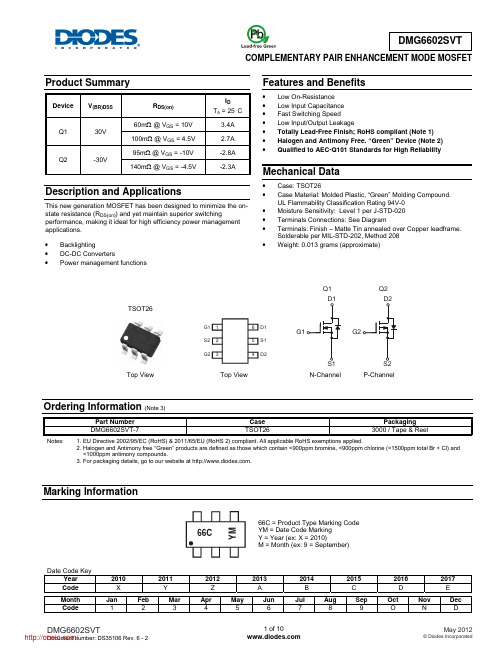
DMG6602SVT-7;中文规格书,Datasheet资料
COMPLEMENTARY PAIR ENHANCEMENT MODE MOSFETProduct SummaryDeviceV (BR)DSSR DS(on)I D T A = 25°C Q1 30V60m Ω @ V GS = 10V3.4A 100m Ω @ V GS =4.5V 2.7A Q2 -30V95m Ω @ V GS = -10V-2.8A 140m Ω @ V GS = -4.5V -2.3ADescription and ApplicationsThis new generation MOSFET has been designed to minimize the on-state resistance (R DS(on)) and yet maintain superior switchingperformance, making it ideal for high efficiency power management applications.• Backlighting • DC-DC Converters • Power management functionsFeatures and Benefits• Low On-Resistance • Low Input Capacitance • Fast Switching Speed • Low Input/Output Leakage • Totally Lead-Free Finish; RoHS compliant (Note 1) • Halogen and Antimony Free. “Green” Device (Note 2) • Qualified to AEC-Q101 Standards for High ReliabilityMechanical Data• Case: TSOT26 • Case Material: Molded Plastic, “Green” Molding Compound.UL Flammability Classification Rating 94V-0 • Moisture Sensitivity: Level 1 per J-STD-020 • Terminals Connections: See Diagram • Terminals: Finish – Matte Tin annealed over Copper leadframe.Solderable per MIL-STD-202, Method 208 • Weight: 0.013 grams (approximate)Ordering Information (Note 3)Part Number Case Packaging DMG6602SVT-7TSOT26 3000 / Tape & ReelNotes:1. EU Directive 2002/95/EC (RoHS) & 2011/65/EU (RoHS 2) compliant. All applicable RoHS exemptions applied.2. Halogen and Antimony free "Green” products are defined as those which contain <900ppm bromine, <900ppm chlorine (<1500ppm total Br + Cl) and <1000ppm antimony compounds.3. For packaging details, go to our website at .Marking InformationDate Code KeyYear 2010 2011 2012 2013 2014 2015 2016 2017Code X Y Z A B C D ETSOT26 Top View Top View 123654D1S1D2G1S2G2N-Channel P-ChannelQ1Q266C = Product Type Marking CodeYM = Date Code MarkingY = Year (ex: X = 2010) M = Month (ex: 9 = September)66C Y MMaximum Ratings – Q1 @TA = 25°C unless otherwise specifiedCharacteristic Symbol Value UnitDrain-Source Voltage V DSS30 V Gate-Source Voltage V GSS±20 VContinuous Drain Current (Note 5) V GS = 10V SteadyStateT A= 25°CT A= 70°CI D3.42.7AContinuous Drain Current (Note 5) V GS = 4.5V SteadyStateT A= 25°CT A= 70°CI D2.72.2AMaximum Continuous Body Diode Forward Current (Note 5) I S 1.5 A Pulsed Drain Current (Note 5) I DM25 AMaximum Ratings – Q2 @TA = 25°C unless otherwise specifiedCharacteristic Symbol Value UnitDrain-Source Voltage V DSS-30 V Gate-Source Voltage V GSS±20 VContinuous Drain Current (Note 5) V GS = -10V SteadyStateT A= 25°CT A= 70°CI D-2.8-2.4AContinuous Drain Current (Note 5) V GS = -4.5V SteadyStateT A= 25°CT A= 70°CI D-2.3-2.1AMaximum Continuous Body Diode Forward Current (Note 5) I S -1.5 APulsed Drain Current (Note 5) I D-20 AThermal CharacteristicsCharacteristic SymbolValueUnitsTotal Power Dissipation (Note 4) T A = 25°CP D0.84W T A = 70°C 0.52Thermal Resistance, Junction to Ambient (Note 4) Steady stateRθJA155°C/W t<10s 109Total Power Dissipation (Note 5) T A = 25°CP D1.27W T A = 70°C 0.8Thermal Resistance, Junction to Ambient (Note 5) Steady stateRθJA102°C/W t<10s 71Thermal Resistance, Junction to Case (Note 5) RθJC34Operating and Storage Temperature Range T J, T STG-55 to +150 °C Notes: 4. Device mounted on FR-4 substrate PC board, 2oz copper, with minimum recommended pad layout.5. Device mounted on FR-4 substrate PC board, 2oz copper, with 1inch square copper plate.Electrical Characteristics – Q1 NMOS @ T A = 25°C unless otherwise statedCharacteristicSymbol Min Typ Max Unit Test ConditionOFF CHARACTERISTICS (Note 6) Drain-Source Breakdown Voltage BV DSS 30 - - V V GS = 0V, I D = 250μA Zero Gate Voltage Drain Current I DSS - - 1.0 µA V DS = 24V, V GS = 0V Gate-Source LeakageI GSS - - ±100 nA V GS = ±20V, V DS = 0V ON CHARACTERISTICS (Note 6) Gate Threshold VoltageV GS(th) 1.0 - 2.3 V V DS = V GS , I D = 250μAStatic Drain-Source On-Resistance R DS (ON) - 38 55 60100 m ΩV GS = 10V, I D = 3.1A V GS = 4.5V, I D = 2AForward Transfer Admittance |Y fs | - 4 - S V DS = 5V, I D = 3.1A Diode Forward VoltageV SD - 0.8 1 V V GS = 0V, I S = 1A DYNAMIC CHARACTERISTICS (Note 7) Input Capacitance C iss - 290 400 pF V DS = 15V, V GS = 0V, f = 1.2MHzOutput CapacitanceC oss - 40 80 Reverse Transfer Capacitance C rss - 40 80 Gate ResistanceR g - 1.4 - Ω V DS = 0V, V GS = 0V, f = 1MHz Total Gate Charge (V GS = 4.5V) Q g - 4 6 nCV DS = 15V, V GS = 4.5V, I D = 3.1A Total Gate Charge (V GS = 10V) Q g - 9 13V DS = 15V, V GS = 10V, I D = 3AGate-Source Charge Q gs - 1.2 - Gate-Drain Charge Q gd - 1.5 - Turn-On Delay Time t D(on) - 3 - nsV GS = 10V, V DS = 15V, R G = 3Ω, R L = 4.7ΩTurn-On Rise Time t r - 5 -Turn-Off Delay Time t D(off) - 13 - Turn-Off Fall Timet f- 3 -Notes:6. Short duration pulse test used to minimize self-heating effect.7. Guaranteed by design. Not subject to product testing.V , DRAIN -SOURCE VOLTAGE(V)Fig. 1 Typical Output CharacteristicsDS I , D R A I N C U R R E N T (A )DV , GATE SOURCE VOLTAGE(V)Fig. 2 Typical Transfer CharacteristicsGS I , D R A I N C U R R E N T (A )D 02468012345I , DRAIN SOURCE CURRENT Fig. 3 Typical On-Resistance vs. Drain Current and Gate VoltageD R ,D R A I N -S O U R CE O N -R E S I S T A N C E ()D S (O N )ΩI , DRAIN SOURCE CURRENT (A)Fig. 4 Typical On-Resistance vs. Drain Current and T emperatureD R , D R A I N -S O U R CE O N -R E S I S T A N C E ()D S (O N )Ω-50-250255075100125150T , JUNCTION TEMPERATURE (C)J °Fig. 5 On-Resistance Variation with TemperatureR , D R A I N -S O U R C E O N -R E S I S T A N C E (N o r m a l i z e d )D S (O N )0.60.811.21.41.6T , JUNCTION TEMPERATURE (C)J °Fig. 6 On-Resistance Variation with Temperature R , D R A I N -S O U R C E O N -R E S I S T A N CED S (O N )00.020.040.060.080.10.40.81.61.22.4V , G A T E T H R E S H O L D V O L T A G E (V )G S (t h )2.0I , S O U R C E C U R R E N T (A )S V , SOURCE-DRAIN VOLTAGE (V)0246810V , DRAIN-SOURCE VOLTAGE (V)Fig. 9 Typical Junction CapacitanceDS C , J U N C T I O N C A P A C I T A N C E (p F )T 1010010002468246810Q (nC)g , TOTAL GATE CHARGE Fig. 10 Gate ChargeV G A T E T H R E S H O L D V O L T A G E (V )G SV , DRAIN-SOURCE VOLTAGE (V)Fig. 11 SOA, Safe Operation AreaDS I , D R A I N C U R R E N T (A )DElectrical Characteristics – Q2 PMOS @ T A = 25°C unless otherwise statedCharacteristicSymbol Min Typ Max Unit Test ConditionOFF CHARACTERISTICS (Note 6) Drain-Source Breakdown Voltage BV DSS -30 - - V V GS = 0V, I D = -250μA Zero Gate Voltage Drain Current I DSS - - -1.0 µA V DS = -24V, V GS = 0V Gate-Source LeakageI GSS - - ±100 nA V GS = ±20V, V DS = 0V ON CHARACTERISTICS (Note 6) Gate Threshold VoltageV GS(th) -1.0 - -2.3 V V DS = V GS , I D = -250μAStatic Drain-Source On-Resistance R DS (ON) - 73 99 95140 m ΩV GS = -10V, I D = -2.7A V GS = -4.5V, I D = -2AForward Transfer Admittance |Y fs | - 6 - S V DS = -5V, I D = -2.7A Diode Forward VoltageV SD - -0.8 -1.0 V V GS = 0V, I S = -1A DYNAMIC CHARACTERISTICS (Note 7) Input Capacitance C iss - 350 420 pF V DS = -15V, V GS = 0V, f = 1.2MHzOutput CapacitanceC oss - 50 100 Reverse Transfer Capacitance C rss - 45 80 Gate ResistanceR g - 17.1 - Ω V DS = 0V, V GS = 0V, f = 1MHz Total Gate Charge (V GS = -4.5V) Q g - 4 6 nCV DS = -15V, V GS = -4.5V, I D = -3A Total Gate Charge (V GS = -10V) Q g - 7 9V DS = -15V, V GS = -10V, I D = -3AGate-Source Charge Q gs - 0.9 - Gate-Drain Charge Q gd - 1.2 - Turn-On Delay Time t D(on) - 4.8 - nsV GS = -10V, V DS = -15V, R G = 6Ω, R L = 15ΩTurn-On Rise Time t r - 7.3 -Turn-Off Delay Time t D(off) - 20 - Turn-Off Fall Timet f- 13 -Notes: 6. Short duration pulse test used to minimize self-heating effect. 7. Guaranteed by design. Not subject to production testing.0.51 1.52 2.53 3.54 4.55V , DRAIN -SOURCE VOLTAGE(V)Fig. 12 Typical Output CharacteristicsDSI , D R A I N C U R R E N TD V , GATE SOURCE VOLTAGE(V)Fig. 13 Typical Transfer CharacteristicsGS I , D R A I N C U R R E N T (A )D 00.51 1.52 2.53 3.54 4.55I , DRAIN SOURCE CURRENT Fig. 14 Typical On-Resistance vs. Drain Current and Gate VoltageD R ,D R A I N -S O U R CE O N -R E S I S T A N C E ()D S (O N )Ω0.10.20.30.402486I , DRAIN SOURCE CURRENT (A)Fig. 15 Typical On-Resistance vs. Drain Current and T emperatureD R , D R A I N -S O U R CE O N -R E S I S T A N C E ()D S (O N )Ω00.040.080.120.160.2-50-250255075100125150T , JUNCTION TEMPERATURE (C)J °Fig. 16 On-Resistance Variation with TemperatureR , D R A I N -S O U R C E O N -R E S I S T A N C E (N o r m a l i z e d )D S (O N )T , JUNCTION TEMPERATURE (C)J °Fig. 17 On-Resistance Variation with TemperatureR , D R A I N -S O U R C E O N -R E S I S T A N C E ()D S (O N )Ω00.40.81.21.6V , G A T E T H R E S H O L D V O L T A G E (V )G S (T H )I , S O U R C E C U R R E N T (V )S 024680.20.40.60.81 1.2 1.4-V , DRAIN-SOURCE VOLTAGE (V)Fig. 20 Typical Junction CapacitanceDS C , J U N C T I O N C A P A C I T A N C E (p F )T51015202530Q (nC)g , TOTAL GATE CHARGE Fig. 21 Gate Charge-V G A T E T H R E S H O L D V O L T A G E (V )G S-V , DRAIN-SOURCE VOLTAGE (V)Fig. 22 SOA, Safe Operation AreaDS -I , D R A I N C U R R E N T (A )D1t1, PULSE DURATION TIME (sec)Fig. 23 Transient Thermal Resistancer (t ), T R A N S I E N T T H E R M A L R E S I S T A N C EPackage Outline DimensionsSuggested Pad LayoutTSOT26Dim Min Max Typ A − 1.00 −A1 0.01 0.10 −A2 0.84 0.90 −D −− 2.90E −− 2.80E1 −− 1.60b 0.30 0.45 −c 0.12 0.20 −e −−0.95e1 −− 1.90L 0.30 0.50L2 −−0.25θ0° 8° 4° θ1 4° 12° −All Dimensions in mmDimensions Value (in mm)C 0.950X 0.700Y 1.000Y1 3.1996x bIMPORTANT NOTICEDIODES INCORPORATED MAKES NO WARRANTY OF ANY KIND, EXPRESS OR IMPLIED, WITH REGARDS TO THIS DOCUMENT, INCLUDING, BUT NOT LIMITED TO, THE IMPLIED WARRANTIES OF MERCHANTABILITY AND FITNESS FOR A PARTICULAR PURPOSE (AND THEIR EQUIVALENTS UNDER THE LAWS OF ANY JURISDICTION).Diodes Incorporated and its subsidiaries reserve the right to make modifications, enhancements, improvements, corrections or other changes without further notice to this document and any product described herein. Diodes Incorporated does not assume any liability arising out of the application or use of this document or any product described herein; neither does Diodes Incorporated convey any license under its patent or trademark rights, nor the rights of others. Any Customer or user of this document or products described herein in such applications shall assume all risks of such use and will agree to hold Diodes Incorporated and all the companies whose products are represented on Diodes Incorporated website, harmless against all damages.Diodes Incorporated does not warrant or accept any liability whatsoever in respect of any products purchased through unauthorized sales channel. Should Customers purchase or use Diodes Incorporated products for any unintended or unauthorized application, Customers shall indemnify and hold Diodes Incorporated and its representatives harmless against all claims, damages, expenses, and attorney fees arising out of, directly or indirectly, any claim of personal injury or death associated with such unintended or unauthorized application.Products described herein may be covered by one or more United States, international or foreign patents pending. Product names and markings noted herein may also be covered by one or more United States, international or foreign trademarks.LIFE SUPPORTDiodes Incorporated products are specifically not authorized for use as critical components in life support devices or systems without the express written approval of the Chief Executive Officer of Diodes Incorporated. As used herein:A. Life support devices or systems are devices or systems which:1. are intended to implant into the body, or2. support or sustain life and whose failure to perform when properly used in accordance with instructions for use provided in thelabeling can be reasonably expected to result in significant injury to the user.B. A critical component is any component in a life support device or system whose failure to perform can be reasonably expected to cause thefailure of the life support device or to affect its safety or effectiveness.Customers represent that they have all necessary expertise in the safety and regulatory ramifications of their life support devices or systems, and acknowledge and agree that they are solely responsible for all legal, regulatory and safety-related requirements concerning their products and any use of Diodes Incorporated products in such safety-critical, life support devices or systems, notwithstanding any devices- or systems-related information or support that may be provided by Diodes Incorporated. Further, Customers must fully indemnify Diodes Incorporated and its representatives against any damages arising out of the use of Diodes Incorporated products in such safety-critical, life support devices or systems.Copyright © 2012, Diodes Incorporated分销商库存信息: DIODESDMG6602SVT-7。
TLP701中文资料
This unit is 6-lead SDIP package. The TLP701 is 50% smaller than the 8-pin DIP and meets the reinforced insulation class requirements of international safety standards. Therefore the mounting area can be reduced in equipment requiring safety standard certification.
4
6: VCC
Schematic
IF 1+ VF 3−
(Tr1)
ICC 6 VCC
IO 5
(Tr2)
VO
SHIELD
4 GND
A 0.1-µF bypass capacitor must be connected
between pins 6 and 4. (See Note 6.)
1
2006-01-17
( Note ) When a EN60747-5-2 approved type is needed, please designate the “Option(D4)”
Truth Table
Input
LED
Tr1
Tr2
Output
H
ON
ON
OFF
H
L
OFF
OFF
ON
L
1.27±0.2 0.4±0.1
三菱 RD01MUS2 说明书
Publication Date:Oct.2011<Silicon RF Power MOS FET (Discrete)>RD01MUS2RoHS Compliance,Silicon MOSFET Power Transistor 520MHz,1WDESCRIPTIONRD01MUS2is a MOS FET type transistor specifically designed for VHF/UHF RF amplifiers applications.This device has an internal monolithic zener diode from gate to source for ESD protection.FEATURES•High power gain:Pout>0.8W,Gp>14dB @Vdd=7.2V,f=520MHz •High Efficiency:65%typ.•Integrated gate protection diodeAPPLICATIONFor output stage of high power amplifiers in VHF/UHF Band mobile radio sets.RoHS COMPLIANTRD01MUS2-101,T113is a RoHS compliant products.This product includes the lead in high melting temperature type solders.However,it is applicable to the following exceptions of RoHS Directions.1.Lead in high melting temperature type solders (i.e.tin-lead solder alloys containing more than85%lead.)ELECTRICAL CHARACTERISTICS(Tc=25°C,UNLESS OTHERWISE NOTED)LIMITS UNITSYMBOL PARAMETERCONDITIONSMIN TYP MAX I DSS Zero gate voltage drain current V DS =17V,V GS =0V --50uA I GSS Gate to source leak current V GS =10V,V DS =0V --1uA Vth Gate threshold Voltage V DS =12V,I DS =1mA 1.3 1.8 2.3V Pout Output power 0.8 1.4-W ηdDrain efficiencyV DD =7.2V,Pin=30mW f=520MHz,Idq=100mA5065-%Note:Above parameters,ratings,limits and conditions are subject to change.OUTLINE DRAWINGLOT No.0.4+/-0.071230.8M I N 0.4+/-0.070.5+/-0.071.5+/-0.10.1MAX1.5+/-0.12.5+/-0.1TYPE NAME1.6+/-0.1φ0.14.4+/-0.1+0.03-0.05Terminal No.1:GATE 2:SOURSE 3:DRAIN UNIT :mm0.43.9+/-0.31.5+/-0.1TYPICAL CHARACTERISTICSTYPICAL CHARACTERISTICSTEST CIRCUIT(f=520MHz)RF-in4mm Note:Boad material Glass epoxi substrateMicro strip line width=1.0mm、50OHM、er:4.8、t=0.6mmL1:Enameled wire 5Turns、D:0.43mm、2.46mmO.D C1、C2:1000pF、0.022μF in parallelINPUT/OUTPUT IMPEDANCE VS.FREQUENCY CHARACTERISTICS520MHz Zin*Zout*Zo=50Vdd=7.2V,Idq=100mA(Vgg adj.),Pin=0.03WZin*=3.11+j11.56Zout*=11.64+j4.74Zin*:Complex conjugate of input impedance Zout*:Complex conjugate of output impedance520MHz Zin*520MHz Zout*ATTENTION:1.High Temperature;This product might have a heat generation while operation,Please take notice that havea possibility to receive a burn to touch the operating product directly or touch the product until cold after switchoff.At the near the product,do not place the combustible material that have possibilities to arise the fire.2.Generation of High Frequency Power;This product generate a high frequency power.Please take noticethat do not leakage the unnecessary electric wave and use this products without cause damage for human and property per normal operation.3.Before use;Before use the product,Please design the equipment in consideration of the risk for human andelectric wave obstacle for equipment.PRECAUTIONS FOR THE USE OF MITSUBISHI SILICON RF POWER DEVICES:1.The specifications of mention are not guarantee values in this data sheet.Please confirm additional detailsregarding operation of these products from the formal specification sheet.For copies of the formal specification sheets,please contact one of our sales offices.2.RA series products(RF power amplifier modules)and RD series products(RF power transistors)are designedfor consumer mobile communication terminals and were not specifically designed for use in other applications.In particular,while these products are highly reliable for their designed purpose,they are not manufactured under a quality assurance testing protocol that is sufficient to guarantee the level of reliability typically deemed necessary for critical communications elements and In the application,which is base station applications and fixed station applications that operate with long term continuous transmission and a higher on-off frequency during transmitting,please consider the derating,the redundancy system,appropriate setting of the maintain period and others as needed.For the reliability report which is described about predicted operating life time of Mitsubishi Silicon RF Products,please contact Mitsubishi Electric Corporation or an authorized Mitsubishi Semiconductor product distributor.3.RD series products use MOSFET semiconductor technology.They are sensitive to ESD voltage thereforeappropriate ESD precautions are required.4.In the case of use in below than recommended frequency,there is possibility to occur that the device isdeteriorated or destroyed due to the RF-swing exceed the breakdown voltage.5.In order to maximize reliability of the equipment,it is better to keep the devices temperature low.It isrecommended to utilize a sufficient sized heat-sink in conjunction with other cooling methods as needed(fan, etc.)to keep the channel temperature for RD series products lower than120deg/C(in case of Tchmax=150deg/C),140deg/C(in case of Tchmax=175deg/C)under standard conditions.6.Do not use the device at the exceeded the maximum rating condition.In case of plastic molded devices,theexceeded maximum rating condition may cause blowout,smoldering or catch fire of the molding resin due to extreme short current flow between the drain and the source of the device.These results causes in fire or injury.7.For specific precautions regarding assembly of these products into the equipment,please refer to thesupplementary items in the specification sheet.8.Warranty for the product is void if the products protective cap(lid)is removed or if the product is modified inany way from it’s original form.9.For additional“Safety first”in your circuit design and notes regarding the materials,please refer the last pageof this data sheet.10.Please refer to the additional precautions in the formal specification sheet.©2011MITSUBISHI ELECTRIC CORPORATION.ALL RIGHTS RESERVED.。
LDMOS的技术和应用
Shekar Mallikarjunaswamy
Shekar M
Alpha & Omega Semiconductor Inc.
1
Technology. Innovation. Powering the Future.
Outline
ldmos的技术和应用 omegasemiconductor inc. applicationsshekar mallikarjunaswamy technology. innovation. powering future.shekar omegasemiconductor inc. powermanagement market drivers ldmostechnology innovations structure,foms; planar, trench, resurf tcadsimulations; device layouts; spice models processintegration cmos/bcdplatforms reliabilityimprovements dc-dc,led, hot-swap, battery protection futuretrends shekar omegasemiconductor inc. $0b$5b $10b $15b $20b $25b $30b 2007 2008 2009 2010 2011 2012 2013 sources: ims july 2010 discrete report (standard mosfets, igbts, igbt modules), ims 2007 power ic report april2009 update power management market growth keydrivers enablingefficient conversion, regulation powershekar omegasemiconductor inc. poweric tam $0m$2,000m $4,000m $6,000m $8,000m $10,000m $12,000m sum tam$$8,068 $8,635 $8,874 $8,382 $9,181 $9,739 $10,245 $10,584 2006 2007 2008 2009 2010 2011 2012 2013 power ic tam $0m$500m $1,000m $1,500m $2,000m $2,500m $3,000m $3,500m tam$ $2,279 $2,455 $2,539 $2,404 $2,646 $2
Omron G3VM-351G1 MOS FET Relays 产品说明书
1Ultrasensitive MOS FET Relays in 350-V Load series for electric power saving.•Trigger LED forward current of 1 mA (maximum) facilitates power saving designs and prolonged battery life.•Continuous load current of 100 mA.■Application Examples■Terminal Arrangement/Internal Connections■List of Models*The AC peak and DC value are given for the load voltage.■Absolute Maximum Ratings (Ta = 25°C)RoHS compliantNote: The actual product is marked differently from theimage shown here.•Communication equipment •Test & Measurement equipment •Security equipment •Amusement equipment •Industrial equipment•Various battery-driven devicesOMRON logo Pin 1 markModel name LOT No.932Mold pin mark *Note:The actual product is marked differently from the image shown here.*The indentation in the corner diagonally opposite from the pin 1 mark is from a pin on the mold.Package type Contact formTerminalsLoad voltage (peak value) *ModelMinimum package quantity Number per tube Number per tape and reelSOP41a(SPST-NO)Surface-mounting Terminals350 VG3VM-351G1100-G3VM-351G1 (TR)-2,500ItemSymbol Rating Unit Measurement conditions I n p u tLED forward current I F 50mANote: 1. The dielectric strength between the input andoutput was checked by applying voltagebetween all pins as a group on the LED side and all pins as a group on the light-receiving side.Repetitive peak LED forward current I FP 1 A 100 µs pulses, 100 pps LED forward current reduction rate ∆I F /°C −0.5 mA/°C Ta ≥ 25°C LED reverse voltage V R 5 V Connection temperature T J 125 °C O u t p u t Load voltage (AC peak/DC)V OFF 350V Continuous load current (AC peak/DC)I O 100mA ON current reduction rate ∆I O /°C −1.0mA/°C Ta ≥ 25°C Connection temperature T J 125°C Dielectric strength between I/O (See note 1.)V I-O 1500Vrms AC for 1 minAmbient operating temperature Ta −40 to +85°C With no icing or condensation Ambient storage temperature Tstg −55 to +125°C With no icing or condensation Soldering temperature -260°C10 s2G3VM-351G1MOS FET Relays■Recommended Operating ConditionsUse the G3VM under the following conditions so that the Relay will operate properly.■Engineering Data■Safety Precautions•Refer to "Common Precautions" for all G3VM models.ItemSymbol MinimumTypicalMaximumUnitLoad voltage (AC peak/DC)V DD --280VOperating LED forward current I F -225 mA Continuous load current (AC peak/DC)I O --80mA Ambient operating temperatureTa−20 -65 °CLED forward current vs. Ambient temperatureContinuous load current vs. Ambient temperatureLED forward current vs. LED forward voltageContinuous load current vs. On-state voltageOn-state resistance vs. Ambient temperatureTrigger LED forward current vs. Ambient temperatureTurn ON, Turn OFF time vs. LED forward currentTurn ON, Turn OFF time vs. Ambient temperatureCurrent leakage vs. AmbienttemperatureI F - TaAmbient temperature Ta (°C)L E D f o r w a r d c u r r e n t I F (m A )0102030405060-40-2020406080100I O- TaAmbient temperature Ta (°C)C o n t i n u o u s l o a d c u r r e n t I O (m A )-40-2020406080100204060801001200I F - V FLED forward voltage V F (V)L E D f o r w a r d c u r r e n t I F (m A )0.11101000.80.91.01.11.21.31.4I O - V ON On-state voltage V ON (V)Co n t i n u o u s l o a d c u r r e n t I O (m A )-150-100-50050100150-3-2-1123R ON - Ta Ambient temperature Ta (°C)O n-s t a t e r e s i s t a n c e R O N (Ω)-40-2020406080100010203040I FT - TaAmbient temperature Ta (°C)T r i g g e r L E D fo r w a r d c u r r e n t I F T (m A )-40-20204060801000.10.20.30.40.50.60.7t ON , t OFF - I F LED forward current I F (mA)T u r n O N , T u r n O F F t i m e t O N , t O F F (m s )0.010.11100.1110100t ON , t OFF - TaAmbient temperature Ta (°C)T u r n O N , T u r n O F F t i m e t O N , t O F F (m s )-40-200204060801000.1110I LEAK - TaAmbient temperature Ta (°C)C u r r e n t l e a k a g e I L E A K (n A )-40-200204060801000.0010.010.1110100■Dimensions(Unit: mm)Note:The actual product is marked differently from the image shown here.Actual Mounting Pad Dimensions(Recommended Value, TOP VIEW)Note: The actual product is marked differently from the image shown here.* The indentation in the corner diagonally opposite from the pin 1 mark is from a pin on the mold.0.4Surface-mounting TerminalsWeight: 0.1 g• Application examples provided in this document are for reference only. In actual applications, confirm equipment functions and safety before using the product.• Consult your OMRON representative before using the product under conditions which are not described in the manual or applying the product to nuclear control systems, railroad systems, aviation systems, vehicles, combustion systems, medical equipment, amusement machines, safety equipment, and other systems or equipment that may have a serious influence on lives and property if used improperly. Make sure that the ratings and performance characteristics of the product provide a margin of safety for the system or equipment, and be sure to provide the system or equipment with double safety mechanisms.Cat. No. K165-E1-010412(0412)(O)Note: Do not use this document to operate the Unit.OMRON CorporationELECTRONIC AND MECHANICAL COMPONENTS COMPANYContact: /ecb。
TLP350
A 0.1 F bypass capacitor must be connected between pins 8 and 5. (See Note 6)
1
2005-08-05
TLP350
Maximum Ratings (Ta 25°C)
Characteristic
Symbol
Rating
Unit
Operating temperature range
Lead soldering temperature (10 s) Isolation voltage (AC, 1 minute, R.H. ≤ 60%)
(Note 4) (Note 5)
IF IF/ Ta IFP VR
Tj IOPH IOPL VCC VCC / Ta
UL Recognized
: UL1577,File No.E67349
Option(D4)
VDE Approved : DIN EN60747-5-2
Maximum Operating Insulation Voltage : 890VPK
Highest Permissible Over Voltage
Forward current
Forward current de-rating (Ta ≥ 85°C)
LE D
Peak transient forward current
(Note 1)
Reverse voltage
Junction temperature
“H” peak output current “L” peak output current
3
2005-08-05
TLP350