74LVC系列
SN74LVC2G04DBVRE4中文资料
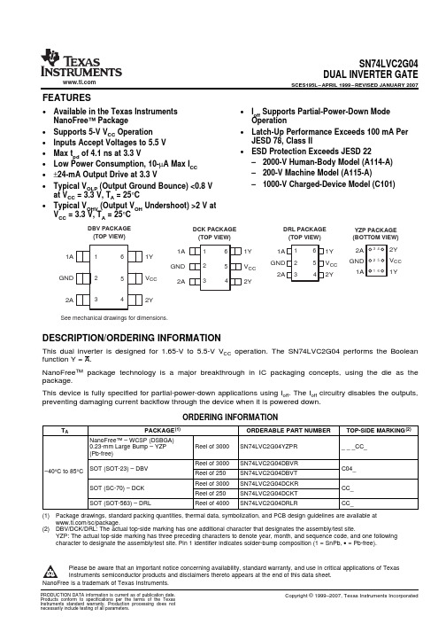
FEATURES1A 1Y2YGND2ADBV PACKAGE (TOP VIEW)YZP PACKAGE (BOTTOM VIEW)DCK PACKAGE (TOP VIEW)1A 1Y 2Y2A1A2A 1Y2Y GND DRL PACKAGE (TOP VIEW)See mechanical drawings for dimensions.V CC V CC CC V CC DESCRIPTION/ORDERING INFORMATIONSN74LVC2G04DUAL INVERTER GATESCES195L–APRIL 1999–REVISED JANUARY 2007•Available in the Texas Instruments •I off Supports Partial-Power-Down Mode NanoFree™PackageOperation•Supports 5-V V CC Operation •Latch-Up Performance Exceeds 100mA Per JESD 78,Class II•Inputs Accept Voltages to 5.5V •ESD Protection Exceeds JESD 22•Max t pd of 4.1ns at 3.3V–2000-V Human-Body Model (A114-A)•Low Power Consumption,10-µA Max I CC –200-V Machine Model (A115-A)•±24-mA Output Drive at 3.3V–1000-V Charged-Device Model (C101)•Typical V OLP (Output Ground Bounce)<0.8V at V CC =3.3V,T A =25°C•Typical V OHV (Output V OH Undershoot)>2V at V CC =3.3V,T A =25°CThis dual inverter is designed for 1.65-V to 5.5-V V CC operation.The SN74LVC2G04performs the Boolean function Y =A.NanoFree™package technology is a major breakthrough in IC packaging concepts,using the die as the package.This device is fully specified for partial-power-down applications using I off .The I off circuitry disables the outputs,preventing damaging current backflow through the device when it is powered down.ORDERING INFORMATIONT APACKAGE (1)ORDERABLE PART NUMBER TOP-SIDE MARKING (2)NanoFree™–WCSP (DSBGA)0.23-mm Large Bump –YZP Reel of 3000SN74LVC2G04YZPR ___CC_(Pb-free)Reel of 3000SN74LVC2G04DBVR SOT (SOT-23)–DBV C04_–40°C to 85°CReel of 250SN74LVC2G04DBVT Reel of 3000SN74LVC2G04DCKR SOT (SC-70)–DCK CC_Reel of 250SN74LVC2G04DCKT SOT (SOT-563)–DRLReel of 4000SN74LVC2G04DRLRCC_(1)Package drawings,standard packing quantities,thermal data,symbolization,and PCB design guidelines are available at /sc/package.(2)DBV/DCK/DRL:The actual top-side marking has one additional character that designates the assembly/test site.YZP:The actual top-side marking has three preceding characters to denote year,month,and sequence code,and one following character to designate the assembly/test site.Pin 1identifier indicates solder-bump composition (1=SnPb,•=Pb-free).Please be aware that an important notice concerning availability,standard warranty,and use in critical applications of Texas Instruments semiconductor products and disclaimers thereto appears at the end of this data sheet.1A1Y2A2YAbsolute Maximum Ratings(1)SN74LVC2G04DUAL INVERTER GATESCES195L–APRIL1999–REVISED JANUARY2007FUNCTION TABLE(EACH INVERTER)INPUT OUTPUTA YH LL HLOGIC DIAGRAM(POSITIVE LOGIC)over operating free-air temperature range(unless otherwise noted)MIN MAX UNIT V CC Supply voltage range–0.5 6.5VV I Input voltage range(2)–0.5 6.5VV O Voltage range applied to any output in the high-impedance or power-off state(2)–0.5 6.5VV O Voltage range applied to any output in the high or low state(2)(3)–0.5V CC+0.5VI IK Input clamp current V I<0–50mAI OK Output clamp current V O<0–50mAI O Continuous output current±50mAContinuous current through V CC or GND±100mADBV package165DCK package259θJA Package thermal impedance(4)°C/WDRL package142YZP package123T stg Storage temperature range–65150°C (1)Stresses beyond those listed under"absolute maximum ratings"may cause permanent damage to the device.These are stress ratingsonly,and functional operation of the device at these or any other conditions beyond those indicated under"recommended operating conditions"is not implied.Exposure to absolute-maximum-rated conditions for extended periods may affect device reliability.(2)The input negative-voltage and output voltage ratings may be exceeded if the input and output current ratings are observed.(3)The value of V CC is provided in the recommended operating conditions table.(4)The package thermal impedance is calculated in accordance with JESD51-7.Recommended Operating Conditions(1)SN74LVC2G04DUAL INVERTER GATESCES195L–APRIL1999–REVISED JANUARY2007MIN MAX UNIT Operating 1.65 5.5V CC Supply voltage VData retention only 1.5V CC=1.65V to1.95V0.65×V CCV CC=2.3V to2.7V 1.7V IH High-level input voltage VV CC=3V to3.6V2V CC=4.5V to5.5V0.7×V CCV CC=1.65V to1.95V0.35×V CCV CC=2.3V to2.7V0.7V IL Low-level input voltage VV CC=3V to3.6V0.8V CC=4.5V to5.5V0.3×V CCV I Input voltage0 5.5V V O Output voltage0V CC VV CC=1.65V–4V CC=2.3V–8I OH High-level output current–16mAV CC=3V–24V CC=4.5V–32V CC=1.65V4V CC=2.3V8I OL Low-level output current16mAV CC=3V24V CC=4.5V32V CC=1.8V±0.15V,2.5V±0.2V20∆t/∆v Input transition rise or fall rate V CC=3.3V±0.3V10ns/VV CC=5V±0.5V5T A Operating free-air temperature–4085°C (1)All unused inputs of the device must be held at V CC or GND to ensure proper device operation.Refer to the TI application report,Implications of Slow or Floating CMOS Inputs,literature number SCBA004.Electrical CharacteristicsSwitching CharacteristicsOperating CharacteristicsSN74LVC2G04DUAL INVERTER GATESCES195L–APRIL 1999–REVISED JANUARY 2007over recommended operating free-air temperature range (unless otherwise noted)PARAMETERTEST CONDITIONSV CC MIN TYP (1)MAX UNIT1.65V to 5.5I OH =–100µA V CC –0.1V I OH =–4mA1.65V 1.2I OH =–8mA2.3V 1.9V OHV I OH =–16mA 2.43V I OH =–24mA 2.3I OH =–32mA 4.5V 3.81.65V to 5.5I OL =100µA 0.1V I OL =4mA1.65V 0.45I OL =8mA2.3V 0.3V OLV I OL =16mA 0.43V I OL =24mA 0.55I OL =32mA4.5V 0.55I I A inputsV I =5.5V or GND 0to 5.5V±5µA I off V I or V O =5.5V 0±10µA 1.65V to 5.5I CC V I =5.5V or GND,I O =010µA V ∆I CC One input at V CC –0.6V,Other inputs at V CC or GND3V to 5.5V 500µA C i V I =V CC or GND3.3V3.5pF (1)All typical values are at V CC =3.3V,T A =25°C.over recommended operating free-air temperature range (unless otherwise noted)(see Figure 1)V CC =1.8V V CC =2.5V V CC =3.3V V CC =5V FROM TO ±0.15V ±0.2V ±0.3V ±0.5V PARAMETERUNIT(INPUT)(OUTPUT)MIN MAXMIN MAX MIN MAX MIN MAX t pdAY3.181.54.41.24.113.2ns T A =25°CV CC =1.8VV CC =2.5VV CC =3.3VV CC =5V PARAMETERTEST CONDITIONSUNIT TYP TYP TYP TYP C pdPower dissipation capacitancef =10MHz14141416pFPARAMETER MEASUREMENT INFORMATIONFrom Output Under TestLOAD CIRCUITOpen Data InputTiming InputV I0 VV I0 V0 VInputVOLTAGE WAVEFORMS SETUP AND HOLD TIMESVOLTAGE WAVEFORMS PROPAGATION DELAY TIMESINVERTING AND NONINVERTING OUTPUTSVOLTAGE WAVEFORMS PULSE DURATIONV OHV OHV OLV OLV I0 V InputOutput Waveform 1S1 at V LOAD (see Note B)Output Waveform 2S1 at GND (see Note B)V OLV OH V LOAD /20 V≈0 VV IVOLTAGE WAVEFORMS ENABLE AND DISABLE TIMES LOW- AND HIGH-LEVEL ENABLINGOutputOutputt PLH /t PHL t PLZ /t PZL t PHZ /t PZHOpen V LOAD GNDTEST S1NOTES: A.C L includes probe and jig capacitance.B.Waveform 1 is for an output with internal conditions such that the output is low, except when disabled by the output control.Waveform 2 is for an output with internal conditions such that the output is high, except when disabled by the output control.C.All input pulses are supplied by generators having the following characteristics: PRR ≤ 10 MHz, Z O = 50 Ω.D.The outputs are measured one at a time, with one transition per measurement.E.t PLZ and t PHZ are the same as t dis .F.t PZL and t PZH are the same as t en .G.t PLH and t PHL are the same as t pd .H.All parameters and waveforms are not applicable to all devices.Output Control V I1.8 V ± 0.15 V2.5 V ± 0.2 V3.3 V ± 0.3 V 5 V ± 0.5 V1 k Ω500 Ω500 Ω500 ΩV CC R L 2 × V CC 2 × V CC 6 V 2 × V CCV LOAD C L 30 pF 30 pF 50 pF 50 pF0.15 V 0.15 V 0.3 V 0.3 VV ∆V CC V CC 3 V V CCV I V CC /2V CC /21.5 V V CC /2V M t r /t f ≤2 ns ≤2 ns ≤2.5 ns ≤2.5 nsINPUTS SN74LVC2G04DUAL INVERTER GATESCES195L–APRIL 1999–REVISED JANUARY 2007Figure 1.Load Circuit and Voltage WaveformsPACKAGING INFORMATIONOrderable Device Status (1)Package Type Package Drawing Pins Package Qty Eco Plan (2)Lead/Ball Finish MSL Peak Temp (3)SN74LVC2G04DBVR ACTIVE SOT-23DBV 63000Green (RoHS &no Sb/Br)CU NIPDAU Level-1-260C-UNLIM SN74LVC2G04DBVRE4ACTIVE SOT-23DBV 63000Green (RoHS &no Sb/Br)CU NIPDAU Level-1-260C-UNLIM SN74LVC2G04DBVT ACTIVE SOT-23DBV 6250Green (RoHS &no Sb/Br)CU NIPDAU Level-1-260C-UNLIM SN74LVC2G04DBVTE4ACTIVE SOT-23DBV 6250Green (RoHS &no Sb/Br)CU NIPDAU Level-1-260C-UNLIM SN74LVC2G04DCKR ACTIVE SC70DCK 63000Green (RoHS &no Sb/Br)CU NIPDAU Level-1-260C-UNLIM SN74LVC2G04DCKRE4ACTIVE SC70DCK 63000Green (RoHS &no Sb/Br)CU NIPDAU Level-1-260C-UNLIM SN74LVC2G04DCKRG4ACTIVE SC70DCK 63000Green (RoHS &no Sb/Br)CU NIPDAU Level-1-260C-UNLIM SN74LVC2G04DCKT ACTIVE SC70DCK 6250Green (RoHS &no Sb/Br)CU NIPDAU Level-1-260C-UNLIM SN74LVC2G04DCKTE4ACTIVE SC70DCK 6250Green (RoHS &no Sb/Br)CU NIPDAU Level-1-260C-UNLIM SN74LVC2G04DCKTG4ACTIVE SC70DCK 6250Green (RoHS &no Sb/Br)CU NIPDAU Level-1-260C-UNLIM SN74LVC2G04DRLR ACTIVE SOT-533DRL 64000Green (RoHS &no Sb/Br)CU NIPDAU Level-1-260C-UNLIM SN74LVC2G04YZPRACTIVEWCSPYZP63000Green (RoHS &no Sb/Br)SNAGCULevel-1-260C-UNLIM(1)The marketing status values are defined as follows:ACTIVE:Product device recommended for new designs.LIFEBUY:TI has announced that the device will be discontinued,and a lifetime-buy period is in effect.NRND:Not recommended for new designs.Device is in production to support existing customers,but TI does not recommend using this part in a new design.PREVIEW:Device has been announced but is not in production.Samples may or may not be available.OBSOLETE:TI has discontinued the production of the device.(2)Eco Plan -The planned eco-friendly classification:Pb-Free (RoHS),Pb-Free (RoHS Exempt),or Green (RoHS &no Sb/Br)-please check /productcontent for the latest availability information and additional product content details.TBD:The Pb-Free/Green conversion plan has not been defined.Pb-Free (RoHS):TI's terms "Lead-Free"or "Pb-Free"mean semiconductor products that are compatible with the current RoHS requirements for all 6substances,including the requirement that lead not exceed 0.1%by weight in homogeneous materials.Where designed to be soldered at high temperatures,TI Pb-Free products are suitable for use in specified lead-free processes.Pb-Free (RoHS Exempt):This component has a RoHS exemption for either 1)lead-based flip-chip solder bumps used between the die and package,or 2)lead-based die adhesive used between the die and leadframe.The component is otherwise considered Pb-Free (RoHS compatible)as defined above.Green (RoHS &no Sb/Br):TI defines "Green"to mean Pb-Free (RoHS compatible),and free of Bromine (Br)and Antimony (Sb)based flame retardants (Br or Sb do not exceed 0.1%by weight in homogeneous material)(3)MSL,Peak Temp.--The Moisture Sensitivity Level rating according to the JEDEC industry standard classifications,and peak solder temperature.Important Information and Disclaimer:The information provided on this page represents TI's knowledge and belief as of the date that it is provided.TI bases its knowledge and belief on information provided by third parties,and makes no representation or warranty as to the accuracy of such information.Efforts are underway to better integrate information from third parties.TI has taken and continues to take reasonable steps to provide representative and accurate information but may not have conducted destructive testing or chemical analysis on incoming materials and chemicals.TI and TI suppliers consider certain information to be proprietary,and thus CAS numbers and other limited information may not be available for release.4-May-2007In no event shall TI's liability arising out of such information exceed the total purchase price of the TI part(s)at issue in this document sold by TI to Customer on an annualbasis.4-May-2007TAPE AND REELINFORMATION12-May-2007DevicePackage Pins SiteReel Diameter (mm)Reel Width (mm)A0(mm)B0(mm)K0(mm)P1(mm)W (mm)Pin1Quadrant SN74LVC2G04DBVR DBV 6HNT 1809 3.23 3.17 1.3748Q3SN74LVC2G04DBVR DBV 6NFME 00 3.23 3.17 1.3748Q3SN74LVC2G04DBVT DBV 6HNT 1809 3.23 3.17 1.3748Q3SN74LVC2G04DCKR DCK 6HNC 1809 2.24 2.34 1.2248Q3SN74LVC2G04DCKT DCK 6HNT 1809 2.24 2.34 1.2248Q3SN74LVC2G04DRLR DRL 6HNT 1809 1.78 1.780.6948Q3SN74LVC2G04YZPRYZP6ASEK18081.021.520.6648Q1TAPE AND REEL BOX INFORMATIONDevicePackage Pins Site Length (mm)Width (mm)Height (mm)SN74LVC2G04DBVR DBV 6HNT 200.0200.030.0SN74LVC2G04DBVR DBV 6NFME 185.0185.0220.0SN74LVC2G04DBVT DBV 6HNT 200.0200.030.0SN74LVC2G04DCKR DCK 6HNC 205.0200.033.0SN74LVC2G04DCKT DCK 6HNT 200.0200.030.0SN74LVC2G04DRLR DRL 6HNT 201.0192.026.0SN74LVC2G04YZPRYZP6ASEK220.0220.034.012-May-200712-May-2007IMPORTANT NOTICETexas Instruments Incorporated and its subsidiaries(TI)reserve the right to make corrections,modifications,enhancements, improvements,and other changes to its products and services at any time and to discontinue any product or service without notice. Customers should obtain the latest relevant information before placing orders and should verify that such information is current and complete.All products are sold subject to TI’s terms and conditions of sale supplied at the time of order acknowledgment.TI warrants performance of its hardware products to the specifications applicable at the time of sale in accordance with TI’s standard warranty.Testing and other quality control techniques are used to the extent TI deems necessary to support this warranty.Except where mandated by government requirements,testing of all parameters of each product is not necessarily performed.TI assumes no liability for applications assistance or customer product design.Customers are responsible for their products and applications using TI components.To minimize the risks associated with customer products and applications,customers should provide adequate design and operating safeguards.TI does not warrant or represent that any license,either express or implied,is granted under any TI patent right,copyright,mask work right,or other TI intellectual property right relating to any combination,machine,or process in which TI products or services are rmation published by TI regarding third-party products or services does not constitute a license from TI to use such products or services or a warranty or endorsement e of such information may require a license from a third party under the patents or other intellectual property of the third party,or a license from TI under the patents or other intellectual property of TI. Reproduction of information in TI data books or data sheets is permissible only if reproduction is without alteration and is accompanied by all associated warranties,conditions,limitations,and notices.Reproduction of this information with alteration is an unfair and deceptive business practice.TI is not responsible or liable for such altered documentation.Resale of TI products or services with statements different from or beyond the parameters stated by TI for that product or service voids all express and any implied warranties for the associated TI product or service and is an unfair and deceptive business practice.TI is not responsible or liable for any such statements.TI products are not authorized for use in safety-critical applications(such as life support)where a failure of the TI product would reasonably be expected to cause severe personal injury or death,unless officers of the parties have executed an agreement specifically governing such use.Buyers represent that they have all necessary expertise in the safety and regulatory ramifications of their applications,and acknowledge and agree that they are solely responsible for all legal,regulatory and safety-related requirements concerning their products and any use of TI products in such safety-critical applications,notwithstanding any applications-related information or support that may be provided by TI.Further,Buyers must fully indemnify TI and its representatives against any damages arising out of the use of TI products in such safety-critical applications.TI products are neither designed nor intended for use in military/aerospace applications or environments unless the TI products are specifically designated by TI as military-grade or"enhanced plastic."Only products designated by TI as military-grade meet military specifications.Buyers acknowledge and agree that any such use of TI products which TI has not designated as military-grade is solely at the Buyer's risk,and that they are solely responsible for compliance with all legal and regulatory requirements in connection with such use.TI products are neither designed nor intended for use in automotive applications or environments unless the specific TI products are designated by TI as compliant with ISO/TS16949requirements.Buyers acknowledge and agree that,if they use anynon-designated products in automotive applications,TI will not be responsible for any failure to meet such requirements. Following are URLs where you can obtain information on other Texas Instruments products and application solutions:Products ApplicationsAmplifiers Audio /audioData Converters Automotive /automotiveDSP Broadband /broadbandInterface Digital Control /digitalcontrolLogic Military /militaryPower Mgmt Optical Networking /opticalnetworkMicrocontrollers Security /securityLow Power /lpw Telephony /telephonyWirelessVideo&Imaging /videoWireless /wirelessMailing Address:Texas Instruments,Post Office Box655303,Dallas,Texas75265Copyright©2007,Texas Instruments Incorporated。
sn74lvc2t45

FEATURESDCT OR DCU PACKAGE(TOP VIEW)12348765V CCA A1A2GNDV CCB B1B2DIRYZP PACKAGE (BOTTOM VIEW)A1GND B1DIR A2B2V CCAV CCBDESCRIPTION/ORDERING INFORMATION•Available in the Texas Instruments NanoFree™Package•Fully Configurable Dual-Rail Design Allows Each Port to Operate Over the Full 1.65-V to 5.5-V Power-Supply Range•V CC Isolation Feature –If Either V CC Input Is at GND,Both Ports Are in the High-Impedance State•DIR Input Circuit Referenced to V CCA•Low Power Consumption,10-µA Max I CC •±24-mA Output Drive at 3.3V•I off Supports Partial-Power-Down Mode Operation•Max Data Rates–420Mbps (3.3-V to 5-V Translation)–210Mbps (Translate to 3.3V)–140Mbps (Translate to 2.5V)–75Mbps (Translate to 1.8V)•Latch-Up Performance Exceeds 100mA Per JESD 78,Class II•ESD Protection Exceeds JESD 22–4000-V Human-Body Model (A114-A)–200-V Machine Model (A115-A)–1000-V Charged-Device Model (C101)This dual-bit noninverting bus transceiver uses two separate configurable power-supply rails.The A port is designed to track V CCA .V CCA accepts any supply voltage from 1.65V to 5.5V.The B port is designed to track V CCB .V CCB accepts any supply voltage from 1.65V to 5.5V.This allows for universal low-voltage bidirectional translation between any of the 1.8-V,2.5-V,3.3-V,and 5-V voltage nodes.ORDERING INFORMATIONT APACKAGE (1)ORDERABLE PART NUMBER TOP-SIDE MARKING (2)NanoFree –WCSP (DSBGA)Reel of 3000SN74LVC2T45YZPR ___TB_0.23-mm Large Bump –YZP (Pb-free)Reel of 3000SN74LVC2T45DCTR SSOP –DCT CT2___–40°C to 85°CReel of 250SN74LVC2T45DCTT Reel of 3000SN74LVC2T45DCUR VSSOP –DCUCT2_Reel of 250SN74LVC2T45DCUT(1)For the most current package and ordering information,see the Package Option Addendum at the end of this document,or see the TI website at .(2)DCT:The actual top-side marking has three additional characters that designate the year,month,and assembly/test site.DCU:The actual top-side marking has one additional character that designates the assembly/test site.YZP:The actual top-side marking has three preceding characters to denote year,month,and sequence code,and one following character to designate the assembly/test site.Pin 1identifier indicates solder-bump composition (1=SnPb,•=Pb-free).Please be aware that an important notice concerning availability,standard warranty,and use in critical applications of Texas Instruments semiconductor products and disclaimers thereto appears at the end of this data sheet.NanoFree is a trademark of Texas Instruments.PRODUCTION DATA information is current as of publication date.Copyright ©2003–2007,Texas Instruments IncorporatedProducts conform to specifications per the terms of the Texas Instruments standard warranty.Production processing does not necessarily include testing of all parameters.DESCRIPTION/ORDERING INFORMATION (CONTINUED)B1DIRA1V CCA V CCBB2A2DUAL-BIT DUAL-SUPPLY BUS TRANSCEIVERWITH CONFIGURABLE VOLTAGE TRANSLATION AND 3-STATE OUTPUTSSCES516I–DECEMBER 2003–REVISED MARCH 2007The SN74LVC2T45is designed for asynchronous communication between two data buses.The logic levels of the direction-control (DIR)input activate either the B-port outputs or the A-port outputs.The device transmits data from the A bus to the B bus when the B-port outputs are activated,and from the B bus to the A bus when the A-port outputs are activated.The input circuitry on both A and B ports always is active and must have a logic HIGH or LOW level applied to prevent excess I CC and I CCZ .The SN74LVC2T45is designed so that the DIR input circuit is supplied by V CCA .This device is fully specified for partial-power-down applications using I off .The I off circuitry disables the outputs,preventing damaging current backflow through the device when it is powered down.The V CC isolation feature ensures that if either V CC input is at GND,both ports are in the high-impedance state.NanoFree™package technology is a major breakthrough in IC packaging concepts,using the die as the package.FUNCTION TABLE (1)(EACH TRANSCEIVER)INPUT OPERATION DIR L B data to A bus HA data toB bus(1)Input circuits of the data I/Os always are active.LOGIC DIAGRAM (POSITIVE LOGIC)2Submit Documentation FeedbackAbsolute Maximum Ratings(1)over operating free-air temperature range(unless otherwise noted)MIN MAX UNITV CCASupply voltage range–0.5 6.5VV CCBV I Input voltage range(2)–0.5 6.5VV O Voltage range applied to any output in the high-impedance or power-off state(2)–0.5 6.5VA port–0.5V CCA+0.5V O Voltage range applied to any output in the high or low state(2)(3)VB port–0.5V CCB+0.5I IK Input clamp current V I<0–50mAI OK Output clamp current V O<0–50mAI O Continuous output current±50mAContinuous current through V CC or GND±100mADCT package220θJA Package thermal impedance(4)DCU package227°C/WYZP package102T stg Storage temperature range–65150°C (1)Stresses beyond those listed under"absolute maximum ratings"may cause permanent damage to the device.These are stress ratingsonly,and functional operation of the device at these or any other conditions beyond those indicated under"recommended operating conditions"is not implied.Exposure to absolute-maximum-rated conditions for extended periods may affect device reliability.(2)The input and output negative-voltage ratings may be exceeded if the input and output clamp-current ratings are observed.(3)The value of V CC is provided in the recommended operating conditions table.(4)The package thermal impedance is calculated in accordance with JESD51-7.3Submit Documentation FeedbackRecommended Operating Conditions (1)(2)(3)DUAL-BIT DUAL-SUPPLY BUS TRANSCEIVERWITH CONFIGURABLE VOLTAGE TRANSLATION AND 3-STATE OUTPUTSSCES516I–DECEMBER 2003–REVISED MARCH 2007V CCIV CCOMIN MAX UNIT V CCA 1.65 5.5Supply voltageVV CCB1.655.51.65V to 1.95VV CCI ×0.652.3V to 2.7V 1.7High-level V IHData inputs (4)Vinput voltage3V to 3.6V 24.5V to5.5V V CCI ×0.71.65V to 1.95VV CCI ×0.352.3V to 2.7V 0.7Low-level V ILData inputs (4)V input voltage3V to 3.6V 0.84.5V to5.5V V CCI ×0.31.65V to 1.95VV CCA ×0.652.3V to 2.7V 1.7High-level DIRV IHVinput voltage(referenced to V CCA )(5)3V to 3.6V 24.5V to5.5V V CCA ×0.71.65V to 1.95VV CCA ×0.352.3V to 2.7V 0.7Low-level DIRV ILV input voltage (referenced to V CCA )(5)3V to 3.6V 0.84.5V to5.5VV CCA ×0.3V I Input voltage 0 5.5V V OOutput voltageV CCOV 1.65V to 1.95V–42.3V to 2.7V –8I OHHigh-level output currentmA 3V to 3.6V –244.5V to 5.5V –321.65V to 1.95V42.3V to 2.7V 8I OLLow-level output currentmA 3V to 3.6V 244.5V to 5.5V321.65V to 1.95V202.3V to 2.7V 20Data inputsInput transition ∆t/∆v3V to 3.6V 10ns/V rise or fall rate4.5V to5.5V5Control input1.65V to 5.5V5T A Operating free-air temperature–4085°C (1)V CCI is the V CC associated with the input port.(2)V CCO is the V CC associated with the output port.(3)All unused data inputs of the device must be held at V CCI or GND to ensure proper device operation.Refer to the TI application report,Implications of Slow or Floating CMOS Inputs ,literature number SCBA004.(4)For V CCI values not specified in the data sheet,V IH min =V CCI ×0.7V,V IL max =V CCI ×0.3V.(5)For V CCI values not specified in the data sheet,V IH min =V CCA ×0.7V,V IL max =V CCA ×0.3V.4Submit Documentation FeedbackElectrical Characteristics(1)(2)over recommended operating free-air temperature range(unless otherwise noted)(1)V CCO is the V CC associated with the output port.(2)V CCI is the V CC associated with the input port.5Submit Documentation FeedbackSwitching CharacteristicsSwitching CharacteristicsDUAL-BIT DUAL-SUPPLY BUS TRANSCEIVERWITH CONFIGURABLE VOLTAGE TRANSLATION AND 3-STATE OUTPUTSSCES516I–DECEMBER 2003–REVISED MARCH 2007over recommended operating free-air temperature range,V CCA =1.8V ±0.15V (unless otherwise noted)(see Figure 1)V CCB =1.8V V CCB =2.5V V CCB =3.3V V CCB =5V FROM TO ±0.15V ±0.2V ±0.3V ±0.5V PARAMETERUNIT(INPUT)(OUTPUT)MIN MAX MIN MAX MIN MAX MIN MAX t PLH 317.7 2.210.3 1.78.3 1.47.2A B ns t PHL 2.814.3 2.28.5 1.87.1 1.77t PLH 317.7 2.316 2.115.5 1.915.1B A ns t PHL 2.814.3 2.112.9212.6 1.812.2t PHZ 10.630.910.330.510.530.510.729.3DIR A ns t PLZ 7.319.77.519.67.519.5719.4t PHZ 1027.98.414.9 6.511.3 4.18.6DIR B ns t PLZ 6.519.57.212.6 4.39.7 2.17.1t PZH (1)37.228.625.222.2DIR A ns t PZL (1)42.227.823.920.8t PZH (1)37.429.927.826.6DIRBns t PZL (1)45.23937.636.3(1)The enable time is a calculated value,derived using the formula shown in the enable times section.over recommended operating free-air temperature range,V CCA =2.5V ±0.2V (unless otherwise noted)(see Figure 1)V CCB =1.8V V CCB =2.5V V CCB =3.3V V CCB =5V FROM TO ±0.15V ±0.2V ±0.3V ±0.5V PARAMETERUNIT(INPUT)(OUTPUT)MIN MAX MIN MAX MIN MAX MIN MAX t PLH 2.316 1.58.5 1.3 6.4 1.1 5.1A B ns t PHL 2.112.9 1.47.5 1.3 5.40.9 4.6t PLH 2.210.3 1.58.5 1.4817.5B A ns t PHL 2.28.5 1.47.5 1.370.9 6.2t PHZ 6.617.17.116.8 6.816.8 5.216.5DIR A ns t PLZ 5.312.6 5.212.5 4.912.3 4.812.3t PHZ 10.727.98.113.9 5.810.5 3.57.6DIR B ns t PLZ 7.818.9 6.211.2 3.68.9 1.46.2t PZH (1)29.219.716.913.7DIR A ns t PZL (1)36.421.417.513.8t PZH (1)28.62118.717.4DIRBns t PZL (1)3024.322.221.1(1)The enable time is a calculated value,derived using the formula shown in the enable times section.6Submit Documentation FeedbackSwitching CharacteristicsSwitching Characteristicsover recommended operating free-air temperature range,V CCA =3.3V ±0.3V (unless otherwise noted)(see Figure 1)V CCB =1.8V V CCB =2.5V V CCB =3.3V V CCB =5V FROM TO ±0.15V ±0.2V ±0.3V ±0.5V PARAMETERUNIT(INPUT)(OUTPUT)MIN MAX MIN MAXMIN MAX MIN MAX t PLH 2.115.5 1.480.7 5.60.7 4.4A B ns t PHL 212.6 1.370.850.74t PLH 1.78.3 1.3 6.40.7 5.80.6 5.4B A ns t PHL 1.87.1 1.3 5.40.850.7 4.5t PHZ 510.9 5.110.8510.8510.4DIR A ns t PLZ 3.48.4 3.78.4 3.98.1 3.37.8t PHZ 11.227.3813.7 5.810.4 2.97.4DIR B ns t PLZ 9.417.7 5.611.3 4.38.315.6t PZH (1)2617.714.111DIR A ns t PZL (1)34.419.115.411.9t PZH (1)23.916.413.912.2DIRBns t PZL (1)23.517.815.814.4(1)The enable time is a calculated value,derived using the formula shown in the enable times section.over recommended operating free-air temperature range,V CCA =5V ±0.5V (unless otherwise noted)(see Figure 1)V CCB =1.8V V CCB =2.5V V CCB =3.3V V CCB =5V FROM TO ±0.15V ±0.2V ±0.3V ±0.5V PARAMETERUNIT(INPUT)(OUTPUT)MIN MAX MIN MAX MIN MAX MIN MAX t PLH 1.915.117.50.6 5.40.5 3.9A B ns t PHL 1.812.20.9 6.20.7 4.50.5 3.5t PLH 1.47.21 5.10.7 4.40.5 3.9B A ns t PHL 1.770.9 4.60.740.5 3.5t PHZ 2.98.2 2.97.9 2.87.9 2.27.8DIR A ns t PLZ 1.4 6.9 1.3 6.70.7 6.70.7 6.6t PHZ 11.226.17.213.9 5.810.1 1.37.3DIR B ns t PLZ 8.416.951147.715.6t PZH (1)24.116.112.19.5DIR A ns t PZL (1)33.118.514.110.8t PZH (1)2214.212.110.5DIRBns t PZL (1)20.414.112.411.3(1)The enable time is a calculated value,derived using the formula shown in the enable times section.7Submit Documentation FeedbackOperating CharacteristicsDUAL-BIT DUAL-SUPPLY BUS TRANSCEIVERWITH CONFIGURABLE VOLTAGE TRANSLATION AND 3-STATE OUTPUTSSCES516I–DECEMBER 2003–REVISED MARCH 2007T A =25°CV CCA =V CCA =V CCA =V CCA =TEST V CCB =1.8VV CCB =2.5VV CCB =3.3VV CCB =5VPARAMETER UNITCONDITIONS TYP TYP TYP TYP A-port input,3444C L =0pF,B-port output C pdA(1)f =10MHz,pFB-port input,t r =t f =1ns 18192021A-port outputA-port input,18192021C L =0pF,B-port output C pdB(1)f =10MHz,pFB-port input,t r =t f =1ns3444A-port output(1)Power dissipation capacitance per transceiver8Submit Documentation FeedbackPower-Up ConsiderationsA proper power-up sequence always should be followed to avoid excessive supply current,bus contention, oscillations,or other anomalies.To guard against such power-up problems,take the following precautions:1.Connect ground before any supply voltage is applied.2.Power up V CCA.3.V CCB can be ramped up along with or after V CCA.Table1.Typical Total Static Power Consumption(I CCA+I CCB)V CCAV CCB UNIT0V 1.8V 2.5V 3.3V5V0V0<1<1<1<11.8V<1<2<2<222.5V<1<2<2<2<2µA3.3V<1<2<2<2<25V<12<2<2<29Submit Documentation FeedbackTYPICAL CHARACTERISTICS5101520253035t P L H− n s C L − pF5101520253035t PH L − n sC L − pFTYPICAL PROPAGATION DELAY (B to A)vs LOADCAPACITANCE5101520253035t P L H − n sC L − pF5101520253035t P H L− n sC L − pFDUAL-BIT DUAL-SUPPLY BUS TRANSCEIVERWITH CONFIGURABLE VOLTAGE TRANSLATION AND 3-STATE OUTPUTSSCES516I–DECEMBER 2003–REVISED MARCH 2007TYPICAL PROPAGATION DELAY (A to B)vs LOAD CAPACITANCET A =25°C,V CCA =1.8VT A =25°C,V CCA =1.8V10Submit Documentation FeedbackTYPICAL CHARACTERISTICS5t P L H − n s C L − pF5101520253035t P H L − n sC L − pFTYPICAL PROPAGATION DELAY (B to A)vs LOAD CAPACITANCEt P H L− n s C L − pF12345678910t P L H − n sC L − pFSN74LVC2T45DUAL-BIT DUAL-SUPPLY BUS TRANSCEIVERWITH CONFIGURABLE VOLTAGE TRANSLATION AND 3-STATE OUTPUTSSCES516I–DECEMBER 2003–REVISED MARCH 2007TYPICAL PROPAGATION DELAY (A to B)vs LOAD CAPACITANCET A =25°C,V CCA =2.5VT A =25°C,V CCA =2.5VTYPICAL CHARACTERISTICS5101520253035t P L H − n sC L − pFt P H L − n sC L − pFTYPICAL PROPAGATION DELAY (B to A)vs LOAD CAPACITANCEt P L H − n sC L − pFt P H L− n s C L − pF5101520253035SN74LVC2T45DUAL-BIT DUAL-SUPPLY BUS TRANSCEIVERWITH CONFIGURABLE VOLTAGE TRANSLATION AND 3-STATE OUTPUTSSCES516I–DECEMBER 2003–REVISED MARCH 2007TYPICAL PROPAGATION DELAY (A to B)vs LOAD CAPACITANCET A =25°C,V CCA =3.3VT A =25°C,V CCA =3.3VTYPICAL CHARACTERISTICSt P H L − n s C L − pFt P L H − n s C L − pFTYPICAL PROPAGATION DELAY (B to A)vs LOAD CAPACITANCEt P H L − n sC L − pFt P L H − n sC L − pF10SN74LVC2T45DUAL-BIT DUAL-SUPPLY BUS TRANSCEIVERWITH CONFIGURABLE VOLTAGE TRANSLATION AND 3-STATE OUTPUTSSCES516I–DECEMBER 2003–REVISED MARCH 2007TYPICAL PROPAGATION DELAY (A to B)vs LOAD CAPACITANCET A =25°C,V CCA =5VT A =25°C,V CCA =5VPARAMETER MEASUREMENT INFORMATIONV OH V OLLOAD CIRCUIT × V CCOOpenOutput Control (low-level enabling)Output Waveform 1S1 at 2 × V CCO (see Note B)Output Waveform 2S1 at GND (see Note B)0 V0 VV CCI0 VV CCAV CCOVOLTAGE WAVEFORMS PROPAGATION DELAY TIMESVOLTAGE WAVEFORMS PULSE DURATIONVOLTAGE WAVEFORMS ENABLE AND DISABLE TIMESInputt pd t PLZ /t PZL t PHZ /t PZHOpen 2 × V CCO GNDTEST S1NOTES: A.C L includes probe and jig capacitance.B.Waveform 1 is for an output with internal conditions such that the output is low, except when disabled by the output control.Waveform 2 is for an output with internal conditions such that the output is high, except when disabled by the output control.C.All input pulses are supplied by generators having the following characteristics: PRR v 10 MHz, Z O = 50 Ω, dv/dt ≥ 1 V/ns.D.The outputs are measured one at a time, with one transition per measurement.E.t PLZ and t PHZ are the same as t dis .F.t PZL and t PZH are the same as t en .G.t PLH and t PHL are the same as t pd .H.V CCI is the V CC associated with the input port.I.V CCO is the V CC associated with the output port.J.All parameters and waveforms are not applicable to all devices.1.8 V ± 0.15 V2.5 V ± 0.2 V3.3 V ± 0.3 V 5 V ± 0.5 V2 k Ω2 k Ω2 k Ω2 k ΩV CCO R L 0.15 V 0.15 V 0.3 V 0.3 VV TP C L 15 pF 15 pF 15 pF 15 pFSN74LVC2T45DUAL-BIT DUAL-SUPPLY BUS TRANSCEIVERWITH CONFIGURABLE VOLTAGE TRANSLATION AND 3-STATE OUTPUTSSCES516I–DECEMBER 2003–REVISED MARCH 2007Figure 1.Load Circuit and Voltage WaveformsAPPLICATION INFORMATIONSYSTEM-1SYSTEM-2SN74LVC2T45DUAL-BIT DUAL-SUPPLY BUS TRANSCEIVERWITH CONFIGURABLE VOLTAGE TRANSLATION AND 3-STATE OUTPUTSSCES516I–DECEMBER 2003–REVISED MARCH 2007The following shows an example of the SN74LVC2T45being used in a unidirectional logic level-shifting application.PIN NAME FUNCTION DESCRIPTION1V CCA V CC1SYSTEM-1supply voltage (1.65V to 5.5V)2A1OUT1Output level depends on V CC1voltage.3A2OUT2Output level depends on V CC1voltage.4GND GND Device GND5DIR DIR GND (low level)determines B-port to A-port direction.6B2IN2Input threshold value depends on V CC2voltage.7B1IN1Input threshold value depends on V CC2voltage.8V CCBV CC2SYSTEM-2supply voltage (1.65V to 5.5V)Figure 2.Unidirectional Logic Level-Shifting ApplicationAPPLICATION INFORMATIONSYSTEM-1SYSTEM-2Enable TimesSN74LVC2T45DUAL-BIT DUAL-SUPPLY BUS TRANSCEIVERWITH CONFIGURABLE VOLTAGE TRANSLATION AND 3-STATE OUTPUTSSCES516I–DECEMBER 2003–REVISED MARCH 2007Figure 3shows the SN74LVC2T45being used in a bidirectional logic level-shifting application.Since the SN74LVC2T45does not have an output-enable (OE)pin,the system designer should take precautions to avoid bus contention between SYSTEM-1and SYSTEM-2when changing directions.The following table shows data transmission from SYSTEM-1to SYSTEM-2and then from SYSTEM-2to SYSTEM-1.STATE DIR CTRLI/O-1I/O-2DESCRIPTION1H Out In SYSTEM-1data to SYSTEM-2SYSTEM-2is getting ready to send data to SYSTEM-1.I/O-1and I/O-2are disabled.The 2H Hi-Z Hi-Z bus-line state depends on pullup or pulldown.(1)DIR bit is flipped.I/O-1and I/O-2still are disabled.The bus-line state depends on pullup or 3L Hi-Z Hi-Z pulldown.(1)4LInOutSYSTEM-2data to SYSTEM-1(1)SYSTEM-1and SYSTEM-2must use the same conditions,i.e.,both pullup or both pulldown.Figure 3.Bidirectional Logic Level-Shifting ApplicationCalculate the enable times for the SN74LVC2T45using the following formulas:•t PZH (DIR to A)=t PLZ (DIR to B)+t PLH (B to A)•t PZL (DIR to A)=t PHZ (DIR to B)+t PHL (B to A)•t PZH (DIR to B)=t PLZ (DIR to A)+t PLH (A to B)•t PZL (DIR to B)=t PHZ (DIR to A)+t PHL (A to B)In a bidirectional application,these enable times provide the maximum delay from the time the DIR bit is switched until an output is expected.For example,if the SN74LVC2T45initially is transmitting from A to B,then the DIR bit is switched;the B port of the device must be disabled before presenting it with an input.After the B port has been disabled,an input signal applied to it appears on the corresponding A port after the specified propagation delay.PACKAGING INFORMATIONOrderable Device Status (1)Package Type PackageDrawing Pins Package Qty Eco Plan (2)Lead/Ball FinishMSL Peak Temp (3)Samples(Requires Login)SN74LVC2T45DCTR ACTIVE SM8DCT83000Green (RoHS& no Sb/Br)CU NIPDAU Level-1-260C-UNLIM Request Free SamplesSN74LVC2T45DCTRE4ACTIVE SM8DCT83000Green (RoHS& no Sb/Br)CU NIPDAU Level-1-260C-UNLIM Request Free SamplesSN74LVC2T45DCTRG4ACTIVE SM8DCT83000Green (RoHS& no Sb/Br)CU NIPDAU Level-1-260C-UNLIM Request Free SamplesSN74LVC2T45DCTT ACTIVE SM8DCT8250Green (RoHS& no Sb/Br)CU NIPDAU Level-1-260C-UNLIM Contact TI Distributoror Sales OfficeSN74LVC2T45DCTTE4ACTIVE SM8DCT8250Green (RoHS& no Sb/Br)CU NIPDAU Level-1-260C-UNLIM Contact TI Distributoror Sales OfficeSN74LVC2T45DCTTG4ACTIVE SM8DCT8250Green (RoHS& no Sb/Br)CU NIPDAU Level-1-260C-UNLIM Contact TI Distributoror Sales OfficeSN74LVC2T45DCUR ACTIVE US8DCU83000Green (RoHS& no Sb/Br)CU NIPDAU Level-1-260C-UNLIM Request Free SamplesSN74LVC2T45DCURE4ACTIVE US8DCU83000Green (RoHS& no Sb/Br)CU NIPDAU Level-1-260C-UNLIM Request Free SamplesSN74LVC2T45DCURG4ACTIVE US8DCU83000Green (RoHS& no Sb/Br)CU NIPDAU Level-1-260C-UNLIM Request Free SamplesSN74LVC2T45DCUT ACTIVE US8DCU8250Green (RoHS& no Sb/Br)CU NIPDAU Level-1-260C-UNLIM Purchase SamplesSN74LVC2T45DCUTE4ACTIVE US8DCU8250Green (RoHS& no Sb/Br)CU NIPDAU Level-1-260C-UNLIM Purchase SamplesSN74LVC2T45DCUTG4ACTIVE US8DCU8250Green (RoHS& no Sb/Br)CU NIPDAU Level-1-260C-UNLIM Purchase SamplesSN74LVC2T45YZPR ACTIVE DSBGA YZP83000Green (RoHS& no Sb/Br)SNAGCU Level-1-260C-UNLIM Request Free Samples(1) The marketing status values are defined as follows:ACTIVE: Product device recommended for new designs.LIFEBUY: TI has announced that the device will be discontinued, and a lifetime-buy period is in effect.NRND: Not recommended for new designs. Device is in production to support existing customers, but TI does not recommend using this part in a new design.PREVIEW: Device has been announced but is not in production. Samples may or may not be available.OBSOLETE: TI has discontinued the production of the device.Addendum-Page 1(2) Eco Plan - The planned eco-friendly classification: Pb-Free (RoHS), Pb-Free (RoHS Exempt), or Green (RoHS & no Sb/Br) - please check /productcontent for the latest availability information and additional product content details.TBD: The Pb-Free/Green conversion plan has not been defined.Pb-Free (RoHS): TI's terms "Lead-Free" or "Pb-Free" mean semiconductor products that are compatible with the current RoHS requirements for all 6 substances, including the requirement that lead not exceed 0.1% by weight in homogeneous materials. Where designed to be soldered at high temperatures, TI Pb-Free products are suitable for use in specified lead-free processes.Pb-Free (RoHS Exempt): This component has a RoHS exemption for either 1) lead-based flip-chip solder bumps used between the die and package, or 2) lead-based die adhesive used between the die and leadframe. The component is otherwise considered Pb-Free (RoHS compatible) as defined above.Green (RoHS & no Sb/Br): TI defines "Green" to mean Pb-Free (RoHS compatible), and free of Bromine (Br) and Antimony (Sb) based flame retardants (Br or Sb do not exceed 0.1% by weight in homogeneous material)(3) MSL, Peak Temp. -- The Moisture Sensitivity Level rating according to the JEDEC industry standard classifications, and peak solder temperature.Important Information and Disclaimer:The information provided on this page represents TI's knowledge and belief as of the date that it is provided. TI bases its knowledge and belief on information provided by third parties, and makes no representation or warranty as to the accuracy of such information. Efforts are underway to better integrate information from third parties. TI has taken and continues to take reasonable steps to provide representative and accurate information but may not have conducted destructive testing or chemical analysis on incoming materials and chemicals. TI and TI suppliers consider certain information to be proprietary, and thus CAS numbers and other limited information may not be available for release.In no event shall TI's liability arising out of such information exceed the total purchase price of the TI part(s) at issue in this document sold by TI to Customer on an annual basis.OTHER QUALIFIED VERSIONS OF SN74LVC2T45 :•Enhanced Product: SN74LVC2T45-EPNOTE: Qualified Version Definitions:•Enhanced Product - Supports Defense, Aerospace and Medical ApplicationsAddendum-Page 2TAPE AND REEL INFORMATION*All dimensions are nominalDevicePackage Type Package Drawing Pins SPQReel Diameter (mm)Reel Width W1(mm)A0(mm)B0(mm)K0(mm)P1(mm)W (mm)Pin1Quadrant SN74LVC2T45YZPR DSBGAYZP83000178.09.21.022.020.634.08.0Q1*All dimensions are nominalDevice Package Type Package Drawing Pins SPQ Length(mm)Width(mm)Height(mm)SN74LVC2T45YZPR DSBGA YZP83000220.0220.035.0IMPORTANT NOTICETexas Instruments Incorporated and its subsidiaries(TI)reserve the right to make corrections,modifications,enhancements,improvements, and other changes to its products and services at any time and to discontinue any product or service without notice.Customers should obtain the latest relevant information before placing orders and should verify that such information is current and complete.All products are sold subject to TI’s terms and conditions of sale supplied at the time of order acknowledgment.TI warrants performance of its hardware products to the specifications applicable at the time of sale in accordance with TI’s standard warranty.Testing and other quality control techniques are used to the extent TI deems necessary to support this warranty.Except where mandated by government requirements,testing of all parameters of each product is not necessarily performed.TI assumes no liability for applications assistance or customer product design.Customers are responsible for their products and applications using TI components.To minimize the risks associated with customer products and applications,customers should provide adequate design and operating safeguards.TI does not warrant or represent that any license,either express or implied,is granted under any TI patent right,copyright,mask work right, or other TI intellectual property right relating to any combination,machine,or process in which TI products or services are rmation published by TI regarding third-party products or services does not constitute a license from TI to use such products or services or a warranty or endorsement e of such information may require a license from a third party under the patents or other intellectual property of the third party,or a license from TI under the patents or other intellectual property of TI.Reproduction of TI information in TI data books or data sheets is permissible only if reproduction is without alteration and is accompanied by all associated warranties,conditions,limitations,and notices.Reproduction of this information with alteration is an unfair and deceptive business practice.TI is not responsible or liable for such altered rmation of third parties may be subject to additional restrictions.Resale of TI products or services with statements different from or beyond the parameters stated by TI for that product or service voids all express and any implied warranties for the associated TI product or service and is an unfair and deceptive business practice.TI is not responsible or liable for any such statements.TI products are not authorized for use in safety-critical applications(such as life support)where a failure of the TI product would reasonably be expected to cause severe personal injury or death,unless officers of the parties have executed an agreement specifically governing such use.Buyers represent that they have all necessary expertise in the safety and regulatory ramifications of their applications,and acknowledge and agree that they are solely responsible for all legal,regulatory and safety-related requirements concerning their products and any use of TI products in such safety-critical applications,notwithstanding any applications-related information or support that may be provided by TI.Further,Buyers must fully indemnify TI and its representatives against any damages arising out of the use of TI products in such safety-critical applications.TI products are neither designed nor intended for use in military/aerospace applications or environments unless the TI products are specifically designated by TI as military-grade or"enhanced plastic."Only products designated by TI as military-grade meet military specifications.Buyers acknowledge and agree that any such use of TI products which TI has not designated as military-grade is solely at the Buyer's risk,and that they are solely responsible for compliance with all legal and regulatory requirements in connection with such use. TI products are neither designed nor intended for use in automotive applications or environments unless the specific TI products are designated by TI as compliant with ISO/TS16949requirements.Buyers acknowledge and agree that,if they use any non-designated products in automotive applications,TI will not be responsible for any failure to meet such requirements.Following are URLs where you can obtain information on other Texas Instruments products and application solutions:Products ApplicationsAudio /audio Communications and Telecom /communicationsAmplifiers Computers and Peripherals /computersData Converters Consumer Electronics /consumer-appsDLP®Products Energy and Lighting /energyDSP Industrial /industrialClocks and Timers /clocks Medical /medicalInterface Security /securityLogic Space,Avionics and Defense /space-avionics-defense Power Mgmt Transportation and /automotiveAutomotiveMicrocontrollers Video and Imaging /videoRFID Wireless /wireless-appsRF/IF and ZigBee®Solutions /lprfTI E2E Community Home Page Mailing Address:Texas Instruments,Post Office Box655303,Dallas,Texas75265Copyright©2011,Texas Instruments Incorporated。
74LVC2G53资料
74LVC2G532-channel analog multiplexer/demultiplexerRev. 03 — 28 August 2007Product data sheet1.General descriptionThe 74LVC2G53 is a low-power, low-voltage, high-speed, Si-gate CMOS device.The 74LVC2G53 provides one analog multiplexer/demultiplexer with a digital selectinput(S),two independent inputs/outputs(Y0and Y1),a common input/output(Z)and anactive LOW enable input (E). When pin E is HIGH, the switch is turned off.Schmitt-trigger action at the select and enable inputs makes the circuit tolerant of slowerinput rise and fall times across the entire V CC range from 1.65 V to 5.5 V.2.Featuress Wide supply voltage range from 1.65V to 5.5Vs Very low ON resistance:x7.5Ω (typical) at V CC=2.7Vx6.5Ω (typical) at V CC=3.3Vx6Ω (typical) at V CC=5Vs Switch current capability of 32 mAs High noise immunitys CMOS low-power consumptions TTL interface compatibility at 3.3 Vs Latch-up performance meets requirements of JESD 78 Class Is ESD protection:x HBM JESD22-A114E exceeds 2000Vx MM JESD22-A115-A exceeds 200Vx CDM JESD22-C101C exceeds 1000Vs Control inputs accepts voltages up to 5 Vs Multiple package optionss Specified from−40°C to +85°C and from−40°C to +125°C3.Ordering information4.Marking5.Functional diagramTable 1.Ordering informationType numberPackageTemperature range NameDescriptionVersion 74LVC2G53DP −40°C to +125°C TSSOP8plastic thin shrink small outline package; 8 leads;body width 3 mm; lead length 0.5 mmSOT505-274LVC2G53DC −40°C to +125°C VSSOP8plastic very thin shrink small outline package; 8 leads;body width 2.3 mm SOT765-174LVC2G53GT −40°C to +125°C XSON8plastic extremely thin small outline package; no leads;8terminals; body 1× 1.95× 0.5 mmSOT833-174LVC2G53GM −40°C to +125°CXQFN8plastic extremely thin quad flat package; no leads;8terminals; body 1.6×1.6×0.5mmSOT902-1Table 2.MarkingType number Marking code 74LVC2G53DC V5374LVC2G53DP V5374LVC2G53GT V5374LVC2G53GMV53Fig 1.Logic symbol001aad386S Z EY0Y167251Fig 2.Logic diagram001aad387ZY0SY1E6.Pinning information6.1Pinning6.2Pin descriptionFig 3.Pin configuration SOT505-2 (TSSOP8) andSOT765-1 (VSSOP8)Fig 4.Pin configuration SOT833-1 (XSON8)74LVC2G53Z V CC E Y0GND Y1GNDS001aae7981234658774LVC2G53Y1Y0V CCSGNDE ZGND001aae80036271845Transparent top viewFig 5.Pin configuration SOT902-1 (XQFN8)001aag724EY1ZV C C GNDY0G N DS Transparent top view36415872terminal 1index area74LVC2G53Table 3.Pin description Symbol PinDescriptionSOT505-2, SOT765-1 and SOT833-1SOT902-1Z 17common output or input E 26enable input (active LOW)GND 35ground (0V)GND 44ground (0V)S53select inputTable 3.Pin description …continuedSymbol Pin DescriptionSOT505-2, SOT765-1 and SOT833-1SOT902-1Y162independent input or outputY071independent input or outputV CC88supply voltage7.Functional descriptionTable 4.Function table[1]Input Channel onS EL L Y0 to Z or Z to Y0H L Y1 to Z or Z to Y1X H Z (switch off)[1]H=HIGH voltage level;L=LOW voltage level;X=don’t care;Z=high-impedance OFF-state.8.Limiting valuesTable 5.Limiting valuesIn accordance with the Absolute Maximum Rating System (IEC 60134). Voltages are referenced to GND (ground = 0 V). Symbol Parameter Conditions Min Max Unit V CC supply voltage−0.5+6.5VV I input voltage[1]−0.5+6.5VI IK input clamping current V I<−0.5V or V I>V CC + 0.5 V−50-mAI SK switch clamping current V I<−0.5V or V I>V CC + 0.5 V-±50mAV SW switch voltage enable and disable mode[2]−0.5V CC + 0.5VI SW switch current V SW>−0.5V or V SW< V CC + 0.5 V-±50mAI CC supply current-100mAI GND ground current−100-mAT stg storage temperature−65+150°CP tot total power dissipation T amb=−40°C to+125°C[3]-250mW[1]The minimum input voltage rating may be exceeded if the input current rating is observed.[2]The minimum and maximum switch voltage ratings may be exceeded if the switch clamping current rating is observed.[3]For the TSSOP8 and VSSOP8 packages: above 110°C the value of P tot derates linearly with 8mW/K.For XSON8 and XQFN8 packages: above 45°C the value of P tot derates linearly with 2.4mW/K.9.Recommended operating conditions[1]To avoid sinking GND current from terminal Z when switch current flows in terminal Yn, the voltage drop across the bidirectional switch must not exceed 0.4V .If the switch current flows into terminal Z,no GND current will flow from terminal Yn.In this case,there is no limit for the voltage drop across the switch.[2]Applies to control signal levels.10.Static characteristicsTable 6.Recommended operating conditions Symbol Parameter Conditions Min Typ Max Unit V CC supply voltage 1.65- 5.5V V I input voltage 0- 5.5V V SW switch voltage enable and disable mode[1]0-V CC V T amb ambient temperature−40-+125°C ∆t/∆Vinput transition rise and fall rateV CC =1.65V to 2.7V [2]--20ns/V V CC =2.7V to 5.5V[2]--10ns/VTable 7.Static characteristicsAt recommended operating conditions; voltages are referenced to GND (ground 0V).Symbol Parameter Conditions−40°C to +85°C −40°C to +125°C Min Typ [1]Max Min Max Unit V IHHIGH-level input voltageV CC =1.65V to 1.95V 0.65V CC--0.65V CC-V V CC =2.3V to 2.7V 1.7-- 1.7-V V CC =3V to 3.6V 2.0-- 2.0-V V CC =4.5V to 5.5V0.7V CC--0.7V CC-V V ILLOW-level input voltageV CC =1.65V to 1.95V --0.35V CC-0.35V CC VV CC =2.3V to 2.7V --0.7-0.7V V CC =3V to 3.6V --0.8-0.8V V CC =4.5V to 5.5V--0.3V CC 0.3V CC V I Iinput leakage current pin S and pin E;V I =5.5V or GND;V CC =0V to 5.5V[2]-±0.1±2-±10µAI S(OFF)OFF-state leakage current V I = V IH or V IL ; V CC =5.5V;see Figure 6[2]-±0.1±5-±20µAI S(ON)ON-state leakage currentV I = V IH or V IL ; V CC =5.5V;see Figure 7[2]-±0.1±5-±20µAI CCsupply current V I =5.5 V or GND;V SW =GND or V CC ; I O =0A;V CC =1.65 V to 5.5V [2]-0.110-40µA∆I CCadditional supply current pin S and pin E;V I =V CC −0.6V;I O =0A;V SW =GND or V CC ;V CC =5.5V[2]-5500-5000µA[1]Typical values are measured at T amb =25°C.[2]These typical values are measured at V CC =3.3V10.1Test circuitsC I inputcapacitance - 2.5---pF C S(OFF)OFF-state capacitance - 6.0---pF C S(ON)ON-state capacitance-18---pFTable 7.Static characteristics …continuedAt recommended operating conditions; voltages are referenced to GND (ground 0V).Symbol Parameter Conditions−40°C to +85°C −40°C to +125°C MinTyp [1]Max Min Max Unit V I =V CC or GND; V O =GND or V CC .Fig 6.Test circuit for measuring OFF-state leakage currentV OI S001aad390S ZEY0Y1V CCGNDswitch switch1122V ILV IH S V IHV IH E V IV IL or V IHV IHV I =V CC or GND and V O =open circuit.Fig 7.Test circuit for measuring ON-state leakage currentI S001aad391S ZEY0Y1V CCGNDV IV IL or V IHV ILswitch 12V ILV IH S V ILV IL E V Oswitch1210.2ON resistance[1]Typical values are measured at T amb =25°C and nominal V CC .[2]Flatness is defined as the difference between the maximum and minimum value of ON resistance measured at identical V CC and temperature.Table 8.ON resistanceAt recommended operating conditions; voltages are referenced to GND (ground 0V); for graphs see Figure 9 to Figure 14.Symbol ParameterConditions−40°C to +85°C −40°C to +125°C Unit MinTyp [1]Max Min Max R ON(peak)ON resistance (peak)V I =GND to V CC ; see Figure 8I SW =4mA;V CC =1.65V to 1.95V-34.0130-195ΩI SW =8mA; V CC =2.3V to 2.7V -12.030-45ΩI SW =12mA; V CC =2.7V -10.425-38ΩI SW =24mA; V CC =3V to 3.6V -7.820-30ΩI SW =32mA;V CC =4.5V to 5.5V- 6.215-23ΩR ON(rail)ON resistance (rail)V I =GND; see Figure 8I SW =4mA;V CC =1.65V to 1.95V-8.218-27ΩI SW =8mA; V CC =2.3V to 2.7V -7.116-24ΩI SW =12mA; V CC =2.7V - 6.914-21ΩI SW =24mA; V CC =3V to 3.6V - 6.512-18ΩI SW =32mA;V CC =4.5V to 5.5V - 5.810-15ΩV I =V CC ; see Figure 8I SW =4mA;V CC =1.65V to 1.95V-10.430-45ΩI SW =8mA; V CC =2.3V to 2.7V -7.620-30ΩI SW =12mA; V CC =2.7V -7.018-27ΩI SW =24mA; V CC =3V to 3.6V - 6.115-23ΩI SW =32mA;V CC =4.5V to 5.5V- 4.910-15ΩR ON(flat)ON resistance (flatness)V I =GND to V CC[2]I SW =4mA;V CC =1.65V to 1.95V-26.0---ΩI SW =8mA; V CC =2.3V to 2.7V - 5.0---ΩI SW =12mA; V CC =2.7V - 3.5---ΩI SW =24mA; V CC =3V to 3.6V - 2.0---ΩI SW =32mA;V CC =4.5V to 5.5V-1.5---Ω10.3ON resistance test circuit and graphsR ON = V SW / I SW .Fig 8.Test circuit for measuring ON resistanceI SWV SW001aad392S ZEY0Y1V CCGNDswitch switch1122V IHV IL S V ILV IL E V IV IL or V IHV IL(1)V CC = 1.8 V .(2)V CC = 2.5 V .(3)V CC = 2.7 V .(4)V CC = 3.3 V .(5)V CC = 5.0 V .Fig 9.Typical ON resistance as a function of input voltage; T amb = 25°CV I (V)054231mna67320103040R ON (Ω)(1)(2)(3)(4)(5)(1)T amb =125°C.(2)T amb =85°C.(3)T amb =25°C.(4)T amb =−40°C.(1)T amb =125°C.(2)T amb =85°C.(3)T amb =25°C.(4)T amb =−40°C.Fig 10.ON resistance as a function of input voltage;V CC =1.8V Fig 11.ON resistance as a function of input voltage;V CC =2.5VV I (V)0 2.01.60.8 1.20.4001aaa7122535154555R ON (Ω)5(4)(3)(2)(1)V I (V)0 2.52.01.0 1.50.5001aaa70891171315R ON (Ω)5(1)(2)(3)(4)(1)T amb =125°C.(2)T amb =85°C.(3)T amb =25°C.(4)T amb =−40°C.(1)T amb =125°C.(2)T amb =85°C.(3)T amb =25°C.(4)T amb =−40°C.Fig 12.ON resistance as a function of input voltage;V CC =2.7V Fig 13.ON resistance as a function of input voltage;V CC =3.3V001aaa709V I (V)0 3.02.01.02.51.50.5971113R ON (Ω)5(1)(2)(3)(4)V I (V)04312001aaa7106810R ON (Ω)4(1)(2)(3)(4)11.Dynamic characteristics(1)T amb =125°C.(2)T amb =85°C.(3)T amb =25°C.(4)T amb =−40°C.Fig 14.ON resistance as a function of input voltage; V CC =5.0VV I (V)054231001aaa7115467R ON (Ω)3(2)(4)(1)(3)Table 9.Dynamic characteristicsAt recommended operating conditions; voltages are referenced to GND (ground =0V); for load circuit see Figure 17.Symbol Parameter Conditions−40°C to +85°C −40°C to +125°C Unit MinTyp [1]Max Min Max t pdpropagation delay Z to Yn or Yn to Z; see Figure 15[2][3]V CC = 1.65 V to 1.95 V --2- 2.5ns V CC = 2.3 V to 2.7 V -- 1.2- 1.5ns V CC = 2.7 V -- 1.0- 1.25ns V CC = 3.0 V to 3.6 V --0.8- 1.0ns V CC = 4.5 V to 5.5 V--0.6-0.8nsTable 9.Dynamic characteristics …continuedAt recommended operating conditions; voltages are referenced to GND (ground=0V); for load circuit see Figure17. Symbol Parameter Conditions−40°C to+85°C−40°C to+125°C UnitMin Typ[1]Max Min Maxt en enable time S to Z or Yn; see Figure16[4]V CC = 1.65 V to 1.95 V 2.6 6.710.3 2.612.9nsV CC = 2.3 V to 2.7 V 1.9 4.1 6.4 1.98.0nsV CC = 2.7 V 1.9 4.0 5.5 1.87.0nsV CC = 3.0 V to 3.6 V 1.8 3.4 5.0 1.8 6.3nsV CC = 4.5 V to 5.5 V 1.3 2.6 3.8 1.3 4.8nsE to Z or Yn; see Figure16[4]V CC = 1.65 V to 1.95 V 1.9 4.07.3 1.99.2nsV CC = 2.3 V to 2.7 V 1.4 2.5 4.4 1.4 5.5nsV CC = 2.7 V 1.1 2.6 3.9 1.1 4.9nsV CC = 3.0 V to 3.6 V 1.2 2.2 3.8 1.2 4.8nsV CC = 4.5 V to 5.5 V 1.0 1.7 2.6 1.0 3.3ns t dis disable time S to Z or Yn; see Figure16[5]V CC = 1.65 V to 1.95 V 2.1 6.810.0 2.112.5nsV CC = 2.3 V to 2.7 V 1.4 3.7 6.1 1.47.7nsV CC = 2.7 V 1.4 4.9 6.2 1.47.8nsV CC = 3.0 V to 3.6 V 1.1 4.0 5.4 1.1 6.8nsV CC = 4.5 V to 5.5 V 1.0 2.9 3.8 1.0 4.8nsE to Z or Yn; see Figure16[5]V CC = 1.65 V to 1.95 V 2.3 5.68.6 2.311.0nsV CC = 2.3 V to 2.7 V 1.2 3.2 4.8 1.2 6.0nsV CC = 2.7 V 1.4 4.0 5.2 1.4 6.5nsV CC = 3.0 V to 3.6 V 2.0 3.7 5.0 2.0 6.3nsV CC = 4.5 V to 5.5 V 1.3 2.9 3.8 1.3 4.8ns[1]Typical values are measured at T amb=25°C and nominal V CC.[2]t pd is the same as t PLH and t PHL.[3]propagation delay is the calculated RC time constant of the typical ON resistance of the switch and the specified capacitance whendriven by an ideal voltage source (zero output impedance).[4]t en is the same as t PZH and t PZL[5]t dis is the same as t PLZ and t PHZ11.1Waveforms and test circuitsMeasurement points are given in Table 10.Logic levels: V OL and V OH are typical output voltage levels that occur with the output load.Fig 15.Input (Yn or Z) to output (Z or Yn) propagation delayst PLHt PHLV M V M V MV MGNDV IV OHV OLYn or Z inputZ or Yn output001aac361Measurement points are given in Table 10.Logic levels: V OL and V OH are typical output voltage levels that occur with the output load.Fig 16.Enable and disable times V M V IGNDV CCV OL V OHGNDS, E inputoutputLOW to OFF OFF to LOWoutputHIGH to OFF OFF to HIGHV M001aad393V Mt PZLt PHZt PZHV XV Yswitch disabledswitch enabledswitch enabledZ, YnZ, Ynt PLZTable 10.Measurement pointsSupply voltageInput Output V CCV M V M V XV Y1.65V to2.7V 0.5V CC 0.5V CC V OL +0.15V V OH −0.15V 2.7V to 5.5V0.5V CC0.5V CCV OL +0.3VV OH −0.3V11.2Additional dynamic characteristicsTest data is given in T able 11.Definitions test circuit:R T = Termination resistance (should be equal to output impedance Z o of the pulse generator).C L = Load capacitance (including jig and probe capacitance).R L = Load resistance.V EXT = External voltage for measuring switching times.Fig 17.Load circuit for switching times V EXTV CCV IV Omna616DUTC L R TR LR LGTable 11.Test dataSupply voltageInput Load V EXT V CCV I t r , t f C L R L t PLH , t PHL t PZH , t PHZ t PZL , t PLZ 1.65V to 1.95V V CC ≤2.0ns 30pF 1k Ωopen GND 2V CC 2.3V to 2.7V V CC ≤2.0ns 30pF 500Ωopen GND 2V CC 2.7V V CC ≤2.5ns 50pF 500Ωopen GND 2V CC 3V to 3.6V V CC ≤2.5ns 50pF 500Ωopen GND 2V CC 4.5V to 5.5VV CC≤2.5ns50pF500ΩopenGND2V CCTable 12.Additional dynamic characteristicsAt recommended operating conditions; voltages are referenced to GND (ground =0V); T amb =25°C.Symbol ParameterConditionsMinTypMaxUnitTHDtotal harmonic distortionf i =600 Hz to 20kHz; R L =600Ω;C L =50pF; V I =0.5V (p-p);see Figure 18V CC =1.65V -0.260-%V CC =2.3V -0.078-%V CC =3.0V -0.078-%V CC =4.5V-0.078-%f (-3dB)−3 dB frequency response R L =50Ω; C L =5pF; see Figure 19V CC =1.65V -200-MHz V CC =2.3V -300-MHz V CC =3.0V -300-MHz V CC =4.5V-300-MHz11.3Test circuitsαisoisolation (OFF-state)R L =50Ω; C L =5pF; f i =10MHz;see Figure 20V CC =1.65V -−42-dB V CC =2.3V -−42-dB V CC =3.0V -−40-dB V CC =4.5V-−40-dBQ injcharge injectionC L =0.1 nF; V gen =0V; R gen =0Ω;f i =1MHz; R L =1M Ω; see Figure 21V CC =1.8V - 3.3-pC V CC =2.5V - 4.1-pC V CC =3.3V - 5.0-pC V CC =4.5V - 6.4-pC V CC =5.5V-7.5-pCTable 12.Additional dynamic characteristics …continuedAt recommended operating conditions; voltages are referenced to GND (ground =0V); T amb =25°C.Symbol ParameterConditionsMinTypMaxUnitFig 18.Test circuit for measuring total harmonic distortionD001aad394600 Ω10 µF0.1 µFSZY0Y1V CC0.5V CCGNDC LR Lswitch switch1122V IHV IL S V ILV IL E f iV IL or V IHEV ILAdjust f i voltage to obtain 0dBm level at output. Increase f i frequency until dB meter reads −3dB.Fig 19.Test circuit for measuring the frequency response when switch is in ON-statedB001aad39550 Ω0.1 µFSZEY0Y1V CC 0.5V CCGNDC LR Lswitch switch1122V IHV IL S V ILV IL E f iV IL or V IHV ILAdjust f i voltage to obtain 0dBm level at input.Fig 20.Test circuit for measuring isolation (OFF-state)dB001aad39650 ΩR L0.1 µFSZEY0Y1V CC0.5V CC0.5V CCGNDC LR Lswitchswitch1122V ILV IH S V IHV IH E f iV IL or V IHV IHa.T est circuitb.Input and output pulse definitionsQ inj =∆V O ×C L .∆V O = output voltage variation.R gen = generator resistance.V gen = generator voltage.Fig 21.Test circuit for measuring charge injection001aad398S ZY0Y1R L C LV CC GNDR genV genswitch12V I V O EV IL G001aac478∆V Ooffon off logicinputV O(S)12.Package outlineFig 22.Package outline SOT505-2 (TSSOP8)UNIT A 1A max.A 2A 3b p L H E L p w y v c e D (1)E (1)Z (1)θ REFERENCESOUTLINE VERSION EUROPEAN PROJECTIONISSUE DATE IECJEDEC JEITAmm0.150.000.950.750.380.220.180.083.12.93.12.90.654.13.90.700.358°0°0.130.10.20.5DIMENSIONS (mm are the original dimensions)Note1. Plastic or metal protrusions of 0.15 mm maximum per side are not included.0.470.33SOT505-2- - -02-01-16w Mb pD Ze0.251485θA 2A 1L p (A 3)detail XALH EE cv M AXAy2.5 5 mm0scaleTSSOP8: plastic thin shrink small outline package; 8 leads; body width 3 mm; lead length 0.5 mmSOT505-21.1pin 1 indexFig 23.Package outline SOT765-1 (VSSOP8)UNIT A 1A max.A 2A 3b p L H E L p w y v c e D (1)E (2)Z (1)θ REFERENCESOUTLINE VERSION EUROPEAN PROJECTIONISSUE DATE IECJEDEC JEITAmm0.150.000.850.600.270.170.230.082.11.92.42.20.53.23.00.40.18°0°0.130.10.20.4DIMENSIONS (mm are the original dimensions)Notes1. Plastic or metal protrusions of 0.15 mm maximum per side are not included.2. Plastic or metal protrusions of 0.25 mm maximum per side are not included.0.400.15Q 0.210.19SOT765-1MO-18702-06-07w Mb pD Ze0.121485θA 2A 1QL p(A 3)detail XALH EE cv M AXAy2.5 5 mm0scaleVSSOP8: plastic very thin shrink small outline package; 8 leads; body width 2.3 mm SOT765-11pin 1 indexFig 24.Package outline SOT833-1 (XSON8)terminal 1index areaREFERENCESOUTLINE VERSION EUROPEAN PROJECTIONISSUE DATE IEC JEDEC JEITA SOT833-1- - -MO-252- - -SOT833-104-07-2204-11-09DIMENSIONS (mm are the original dimensions)XSON8: plastic extremely thin small outline package; no leads; 8 terminals; body 1 x 1.95 x 0.5 mm DEe 1eA 1b LL 1e 1e 11 2 mmscaleNotes1. Including plating thickness.2. Can be visible in some manufacturing processes.UNIT mm0.250.172.01.90.350.27A 1max b E 1.050.95D e e 1L 0.400.32L 10.50.6A (1)max 0.50.04182736458×(2)4×(2)AFig 25.Package outline SOT902-1 (XQFN8)REFERENCESOUTLINE VERSION EUROPEAN PROJECTIONISSUE DATE IEC JEDEC JEITA SOT902-1MO-255- - -- - -SOT902-105-11-1605-11-25UNIT A max mm0.5A 10.250.150.050.001.651.550.350.250.150.05DIMENSIONS (mm are the original dimensions)XQFN8: plastic extremely thin quad flat package; no leads; 8 terminals; body 1.6 x 1.6 x 0.5 mm b D L e 11.651.55e E L 1v 0.10.550.5w 0.05y 0.050.05y 101 2 mmscaleXCyCy 1terminal 1index areaterminal 1index areaB ADE detail XAA 1b8765e 1e 1eeA CB ∅ v M C∅ w M 4123LL 1metal area not for soldering13.Abbreviations14.Revision historyTable 13.AbbreviationsAcronym DescriptionCMOS Complementary Metal Oxide Semiconductor TTL T ransistor-Transistor Logic HBM Human Body Model ESD ElectroStatic Discharge MM Machine Model CDM Charged Device Model DUTDevice Under TestTable 14.Revision historyDocument ID Release date Data sheet status Change notice Supersedes 74LVC2G53_320070828Product data sheet-74LVC2G53_2Modifications:•The format of this data sheet has been redesigned to comply with the new identity guidelines of NXP Semiconductors.•Legal texts have been adapted to the new company name where appropriate.•Added type number 74LVC2G53GM (XQFN8/SOT902-1 package).•Section 2 “Features”:Added: Switch handling capability of 32 mA.•Section 10 “Static characteristics”:Changed: Conditions for input leakage and supply current.•Section 11.2 “Additional dynamic characteristics”:Removed: Crosstalk between switches removed from additional characteristics table.Changed: T ypical values of the charge injection.74LVC2G53_220060331Product data sheet -74LVC2G53_174LVC2G53_120060110Product data sheet--74LVC2G53_3© NXP B.V . 2007. All rights reserved.Product data sheet Rev. 03 — 28 August 200721 of 2215.Legal information15.1Data sheet status[1]Please consult the most recently issued document before initiating or completing a design.[2]The term ‘short data sheet’ is explained in section “Definitions”.[3]The product status of device(s)described in this document may have changed since this document was published and may differ in case of multiple devices.The latest product status information is available on the Internet at URL .15.2DefinitionsDraft —The document is a draft version only. The content is still under internal review and subject to formal approval, which may result in modifications or additions. NXP Semiconductors does not give any representations or warranties as to the accuracy or completeness ofinformation included herein and shall have no liability for the consequences of use of such information.Short data sheet —A short data sheet is an extract from a full data sheet with the same product type number(s)and title.A short data sheet is intended for quick reference only and should not be relied upon to contain detailed and full information. For detailed and full information see the relevant full data sheet, which is available on request via the local NXP Semiconductors sales office. In case of any inconsistency or conflict with the short data sheet, the full data sheet shall prevail.15.3DisclaimersGeneral —Information in this document is believed to be accurate andreliable.However,NXP Semiconductors does not give any representations or warranties,expressed or implied,as to the accuracy or completeness of such information and shall have no liability for the consequences of use of such information.Right to make changes —NXP Semiconductors reserves the right to make changes to information published in this document, including withoutlimitation specifications and product descriptions, at any time and without notice.This document supersedes and replaces all information supplied prior to the publication hereof.Suitability for use —NXP Semiconductors products are not designed,authorized or warranted to be suitable for use in medical, military, aircraft,space or life support equipment, nor in applications where failure ormalfunction of a NXP Semiconductors product can reasonably be expected to result in personal injury, death or severe property or environmental damage.NXP Semiconductors accepts no liability for inclusion and/or use of NXP Semiconductors products in such equipment or applications and therefore such inclusion and/or use is at the customer’s own risk.Applications —Applications that are described herein for any of these products are for illustrative purposes only. NXP Semiconductors makes no representation or warranty that such applications will be suitable for the specified use without further testing or modification.Limiting values —Stress above one or more limiting values (as defined in the Absolute Maximum Ratings System of IEC 60134)may cause permanent damage to the device.Limiting values are stress ratings only and operation of the device at these or any other conditions above those given in theCharacteristics sections of this document is not implied. Exposure to limiting values for extended periods may affect device reliability.Terms and conditions of sale —NXP Semiconductors products are sold subject to the general terms and conditions of commercial sale,as published at /profile/terms , including those pertaining to warranty,intellectual property rights infringement and limitation of liability, unless explicitly otherwise agreed to in writing by NXP Semiconductors. In case of any inconsistency or conflict between information in this document and such terms and conditions, the latter will prevail.No offer to sell or license —Nothing in this document may be interpreted or construed as an offer to sell products that is open for acceptance or the grant,conveyance or implication of any license under any copyrights,patents or other industrial or intellectual property rights.15.4TrademarksNotice:All referenced brands,product names,service names and trademarks are the property of their respective owners.16.Contact informationFor additional information, please visit:For sales office addresses, send an email to:salesaddresses@Document status [1][2]Product status [3]DefinitionObjective [short] data sheet Development This document contains data from the objective specification for product development.Preliminary [short] data sheet Qualification This document contains data from the preliminary specification.Product [short] data sheetProductionThis document contains the product specification.17.Contents1General description. . . . . . . . . . . . . . . . . . . . . . 12Features . . . . . . . . . . . . . . . . . . . . . . . . . . . . . . . 13Ordering information. . . . . . . . . . . . . . . . . . . . . 24Marking. . . . . . . . . . . . . . . . . . . . . . . . . . . . . . . . 25Functional diagram . . . . . . . . . . . . . . . . . . . . . . 26Pinning information. . . . . . . . . . . . . . . . . . . . . . 36.1Pinning . . . . . . . . . . . . . . . . . . . . . . . . . . . . . . . 36.2Pin description . . . . . . . . . . . . . . . . . . . . . . . . . 37Functional description . . . . . . . . . . . . . . . . . . . 48Limiting values. . . . . . . . . . . . . . . . . . . . . . . . . . 49Recommended operating conditions. . . . . . . . 510Static characteristics. . . . . . . . . . . . . . . . . . . . . 510.1T est circuits. . . . . . . . . . . . . . . . . . . . . . . . . . . . 610.2ON resistance. . . . . . . . . . . . . . . . . . . . . . . . . . 710.3ON resistance test circuit and graphs. . . . . . . . 811Dynamic characteristics . . . . . . . . . . . . . . . . . 1011.1Waveforms and test circuits . . . . . . . . . . . . . . 1211.2Additional dynamic characteristics . . . . . . . . . 1311.3T est circuits. . . . . . . . . . . . . . . . . . . . . . . . . . . 1412Package outline . . . . . . . . . . . . . . . . . . . . . . . . 1613Abbreviations. . . . . . . . . . . . . . . . . . . . . . . . . . 2014Revision history. . . . . . . . . . . . . . . . . . . . . . . . 2015Legal information. . . . . . . . . . . . . . . . . . . . . . . 2115.1Data sheet status . . . . . . . . . . . . . . . . . . . . . . 2115.2Definitions. . . . . . . . . . . . . . . . . . . . . . . . . . . . 2115.3Disclaimers. . . . . . . . . . . . . . . . . . . . . . . . . . . 2115.4T rademarks. . . . . . . . . . . . . . . . . . . . . . . . . . . 2116Contact information. . . . . . . . . . . . . . . . . . . . . 2117Contents. . . . . . . . . . . . . . . . . . . . . . . . . . . . . . 22Please be aware that important notices concerning this document and the product(s)described herein, have been included in section ‘Legal information’.© NXP B.V.2007.All rights reserved.For more information, please visit: For sales office addresses, please send an email to: salesaddresses@Date of release: 28 August 2007Document identifier: 74LVC2G53_3。
74LVC1G32GF中文资料
For XSON6 packages: above 45 °C the value of Ptot derates linearly with 2.4 mW/K.
9. Recommended operating conditions
Table 6. Symbol VCC VI VO
Tamb ∆t/∆V
SOT353-1
SOT753 SOT886
SOT891
Table 2. Marking Type number 74LVC1G32GW 74LVC1G32GV 74LVC1G32GM 74LVC1G32GF
5. Functional diagram
Marking code VG V32 VG VG
1B 2A
元器件交易网
74LVC1G32
Single 2-input OR gate
Rev. 06 — 2 August 2007
Product data sheet
1. General description
The 74LVC1G32 provides one 2-input OR function.
plastic surface-mounted package; 5 leads
plastic extremely thin small outline package; no leads; 6 terminals; body 1 × 1.45 × 0.5 mm
SN74LVC2G04DBVTE4中文资料

FEATURES1A 1Y2YGND2ADBV PACKAGE (TOP VIEW)YZP PACKAGE (BOTTOM VIEW)DCK PACKAGE (TOP VIEW)1A 1Y 2Y2A1A2A 1Y2Y GND DRL PACKAGE (TOP VIEW)See mechanical drawings for dimensions.V CC V CC CC V CC DESCRIPTION/ORDERING INFORMATIONSN74LVC2G04DUAL INVERTER GATESCES195L–APRIL 1999–REVISED JANUARY 2007•Available in the Texas Instruments •I off Supports Partial-Power-Down Mode NanoFree™PackageOperation•Supports 5-V V CC Operation •Latch-Up Performance Exceeds 100mA Per JESD 78,Class II•Inputs Accept Voltages to 5.5V •ESD Protection Exceeds JESD 22•Max t pd of 4.1ns at 3.3V–2000-V Human-Body Model (A114-A)•Low Power Consumption,10-µA Max I CC –200-V Machine Model (A115-A)•±24-mA Output Drive at 3.3V–1000-V Charged-Device Model (C101)•Typical V OLP (Output Ground Bounce)<0.8V at V CC =3.3V,T A =25°C•Typical V OHV (Output V OH Undershoot)>2V at V CC =3.3V,T A =25°CThis dual inverter is designed for 1.65-V to 5.5-V V CC operation.The SN74LVC2G04performs the Boolean function Y =A.NanoFree™package technology is a major breakthrough in IC packaging concepts,using the die as the package.This device is fully specified for partial-power-down applications using I off .The I off circuitry disables the outputs,preventing damaging current backflow through the device when it is powered down.ORDERING INFORMATIONT APACKAGE (1)ORDERABLE PART NUMBER TOP-SIDE MARKING (2)NanoFree™–WCSP (DSBGA)0.23-mm Large Bump –YZP Reel of 3000SN74LVC2G04YZPR ___CC_(Pb-free)Reel of 3000SN74LVC2G04DBVR SOT (SOT-23)–DBV C04_–40°C to 85°CReel of 250SN74LVC2G04DBVT Reel of 3000SN74LVC2G04DCKR SOT (SC-70)–DCK CC_Reel of 250SN74LVC2G04DCKT SOT (SOT-563)–DRLReel of 4000SN74LVC2G04DRLRCC_(1)Package drawings,standard packing quantities,thermal data,symbolization,and PCB design guidelines are available at /sc/package.(2)DBV/DCK/DRL:The actual top-side marking has one additional character that designates the assembly/test site.YZP:The actual top-side marking has three preceding characters to denote year,month,and sequence code,and one following character to designate the assembly/test site.Pin 1identifier indicates solder-bump composition (1=SnPb,•=Pb-free).Please be aware that an important notice concerning availability,standard warranty,and use in critical applications of Texas Instruments semiconductor products and disclaimers thereto appears at the end of this data sheet.1A1Y2A2YAbsolute Maximum Ratings(1)SN74LVC2G04DUAL INVERTER GATESCES195L–APRIL1999–REVISED JANUARY2007FUNCTION TABLE(EACH INVERTER)INPUT OUTPUTA YH LL HLOGIC DIAGRAM(POSITIVE LOGIC)over operating free-air temperature range(unless otherwise noted)MIN MAX UNIT V CC Supply voltage range–0.5 6.5VV I Input voltage range(2)–0.5 6.5VV O Voltage range applied to any output in the high-impedance or power-off state(2)–0.5 6.5VV O Voltage range applied to any output in the high or low state(2)(3)–0.5V CC+0.5VI IK Input clamp current V I<0–50mAI OK Output clamp current V O<0–50mAI O Continuous output current±50mAContinuous current through V CC or GND±100mADBV package165DCK package259θJA Package thermal impedance(4)°C/WDRL package142YZP package123T stg Storage temperature range–65150°C (1)Stresses beyond those listed under"absolute maximum ratings"may cause permanent damage to the device.These are stress ratingsonly,and functional operation of the device at these or any other conditions beyond those indicated under"recommended operating conditions"is not implied.Exposure to absolute-maximum-rated conditions for extended periods may affect device reliability.(2)The input negative-voltage and output voltage ratings may be exceeded if the input and output current ratings are observed.(3)The value of V CC is provided in the recommended operating conditions table.(4)The package thermal impedance is calculated in accordance with JESD51-7.Recommended Operating Conditions(1)SN74LVC2G04DUAL INVERTER GATESCES195L–APRIL1999–REVISED JANUARY2007MIN MAX UNIT Operating 1.65 5.5V CC Supply voltage VData retention only 1.5V CC=1.65V to1.95V0.65×V CCV CC=2.3V to2.7V 1.7V IH High-level input voltage VV CC=3V to3.6V2V CC=4.5V to5.5V0.7×V CCV CC=1.65V to1.95V0.35×V CCV CC=2.3V to2.7V0.7V IL Low-level input voltage VV CC=3V to3.6V0.8V CC=4.5V to5.5V0.3×V CCV I Input voltage0 5.5V V O Output voltage0V CC VV CC=1.65V–4V CC=2.3V–8I OH High-level output current–16mAV CC=3V–24V CC=4.5V–32V CC=1.65V4V CC=2.3V8I OL Low-level output current16mAV CC=3V24V CC=4.5V32V CC=1.8V±0.15V,2.5V±0.2V20∆t/∆v Input transition rise or fall rate V CC=3.3V±0.3V10ns/VV CC=5V±0.5V5T A Operating free-air temperature–4085°C (1)All unused inputs of the device must be held at V CC or GND to ensure proper device operation.Refer to the TI application report,Implications of Slow or Floating CMOS Inputs,literature number SCBA004.Electrical CharacteristicsSwitching CharacteristicsOperating CharacteristicsSN74LVC2G04DUAL INVERTER GATESCES195L–APRIL 1999–REVISED JANUARY 2007over recommended operating free-air temperature range (unless otherwise noted)PARAMETERTEST CONDITIONSV CC MIN TYP (1)MAX UNIT1.65V to 5.5I OH =–100µA V CC –0.1V I OH =–4mA1.65V 1.2I OH =–8mA2.3V 1.9V OHV I OH =–16mA 2.43V I OH =–24mA 2.3I OH =–32mA 4.5V 3.81.65V to 5.5I OL =100µA 0.1V I OL =4mA1.65V 0.45I OL =8mA2.3V 0.3V OLV I OL =16mA 0.43V I OL =24mA 0.55I OL =32mA4.5V 0.55I I A inputsV I =5.5V or GND 0to 5.5V±5µA I off V I or V O =5.5V 0±10µA 1.65V to 5.5I CC V I =5.5V or GND,I O =010µA V ∆I CC One input at V CC –0.6V,Other inputs at V CC or GND3V to 5.5V 500µA C i V I =V CC or GND3.3V3.5pF (1)All typical values are at V CC =3.3V,T A =25°C.over recommended operating free-air temperature range (unless otherwise noted)(see Figure 1)V CC =1.8V V CC =2.5V V CC =3.3V V CC =5V FROM TO ±0.15V ±0.2V ±0.3V ±0.5V PARAMETERUNIT(INPUT)(OUTPUT)MIN MAXMIN MAX MIN MAX MIN MAX t pdAY3.181.54.41.24.113.2ns T A =25°CV CC =1.8VV CC =2.5VV CC =3.3VV CC =5V PARAMETERTEST CONDITIONSUNIT TYP TYP TYP TYP C pdPower dissipation capacitancef =10MHz14141416pFPARAMETER MEASUREMENT INFORMATIONFrom Output Under TestLOAD CIRCUITOpen Data InputTiming InputV I0 VV I0 V0 VInputVOLTAGE WAVEFORMS SETUP AND HOLD TIMESVOLTAGE WAVEFORMS PROPAGATION DELAY TIMESINVERTING AND NONINVERTING OUTPUTSVOLTAGE WAVEFORMS PULSE DURATIONV OHV OHV OLV OLV I0 V InputOutput Waveform 1S1 at V LOAD (see Note B)Output Waveform 2S1 at GND (see Note B)V OLV OH V LOAD /20 V≈0 VV IVOLTAGE WAVEFORMS ENABLE AND DISABLE TIMES LOW- AND HIGH-LEVEL ENABLINGOutputOutputt PLH /t PHL t PLZ /t PZL t PHZ /t PZHOpen V LOAD GNDTEST S1NOTES: A.C L includes probe and jig capacitance.B.Waveform 1 is for an output with internal conditions such that the output is low, except when disabled by the output control.Waveform 2 is for an output with internal conditions such that the output is high, except when disabled by the output control.C.All input pulses are supplied by generators having the following characteristics: PRR ≤ 10 MHz, Z O = 50 Ω.D.The outputs are measured one at a time, with one transition per measurement.E.t PLZ and t PHZ are the same as t dis .F.t PZL and t PZH are the same as t en .G.t PLH and t PHL are the same as t pd .H.All parameters and waveforms are not applicable to all devices.Output Control V I1.8 V ± 0.15 V2.5 V ± 0.2 V3.3 V ± 0.3 V 5 V ± 0.5 V1 k Ω500 Ω500 Ω500 ΩV CC R L 2 × V CC 2 × V CC 6 V 2 × V CCV LOAD C L 30 pF 30 pF 50 pF 50 pF0.15 V 0.15 V 0.3 V 0.3 VV ∆V CC V CC 3 V V CCV I V CC /2V CC /21.5 V V CC /2V M t r /t f ≤2 ns ≤2 ns ≤2.5 ns ≤2.5 nsINPUTS SN74LVC2G04DUAL INVERTER GATESCES195L–APRIL 1999–REVISED JANUARY 2007Figure 1.Load Circuit and Voltage WaveformsPACKAGING INFORMATIONOrderable Device Status (1)Package Type Package Drawing Pins Package Qty Eco Plan (2)Lead/Ball Finish MSL Peak Temp (3)SN74LVC2G04DBVR ACTIVE SOT-23DBV 63000Green (RoHS &no Sb/Br)CU NIPDAU Level-1-260C-UNLIM SN74LVC2G04DBVRE4ACTIVE SOT-23DBV 63000Green (RoHS &no Sb/Br)CU NIPDAU Level-1-260C-UNLIM SN74LVC2G04DBVT ACTIVE SOT-23DBV 6250Green (RoHS &no Sb/Br)CU NIPDAU Level-1-260C-UNLIM SN74LVC2G04DBVTE4ACTIVE SOT-23DBV 6250Green (RoHS &no Sb/Br)CU NIPDAU Level-1-260C-UNLIM SN74LVC2G04DCKR ACTIVE SC70DCK 63000Green (RoHS &no Sb/Br)CU NIPDAU Level-1-260C-UNLIM SN74LVC2G04DCKRE4ACTIVE SC70DCK 63000Green (RoHS &no Sb/Br)CU NIPDAU Level-1-260C-UNLIM SN74LVC2G04DCKRG4ACTIVE SC70DCK 63000Green (RoHS &no Sb/Br)CU NIPDAU Level-1-260C-UNLIM SN74LVC2G04DCKT ACTIVE SC70DCK 6250Green (RoHS &no Sb/Br)CU NIPDAU Level-1-260C-UNLIM SN74LVC2G04DCKTE4ACTIVE SC70DCK 6250Green (RoHS &no Sb/Br)CU NIPDAU Level-1-260C-UNLIM SN74LVC2G04DCKTG4ACTIVE SC70DCK 6250Green (RoHS &no Sb/Br)CU NIPDAU Level-1-260C-UNLIM SN74LVC2G04DRLR ACTIVE SOT-533DRL 64000Green (RoHS &no Sb/Br)CU NIPDAU Level-1-260C-UNLIM SN74LVC2G04YZPRACTIVEWCSPYZP63000Green (RoHS &no Sb/Br)SNAGCULevel-1-260C-UNLIM(1)The marketing status values are defined as follows:ACTIVE:Product device recommended for new designs.LIFEBUY:TI has announced that the device will be discontinued,and a lifetime-buy period is in effect.NRND:Not recommended for new designs.Device is in production to support existing customers,but TI does not recommend using this part in a new design.PREVIEW:Device has been announced but is not in production.Samples may or may not be available.OBSOLETE:TI has discontinued the production of the device.(2)Eco Plan -The planned eco-friendly classification:Pb-Free (RoHS),Pb-Free (RoHS Exempt),or Green (RoHS &no Sb/Br)-please check /productcontent for the latest availability information and additional product content details.TBD:The Pb-Free/Green conversion plan has not been defined.Pb-Free (RoHS):TI's terms "Lead-Free"or "Pb-Free"mean semiconductor products that are compatible with the current RoHS requirements for all 6substances,including the requirement that lead not exceed 0.1%by weight in homogeneous materials.Where designed to be soldered at high temperatures,TI Pb-Free products are suitable for use in specified lead-free processes.Pb-Free (RoHS Exempt):This component has a RoHS exemption for either 1)lead-based flip-chip solder bumps used between the die and package,or 2)lead-based die adhesive used between the die and leadframe.The component is otherwise considered Pb-Free (RoHS compatible)as defined above.Green (RoHS &no Sb/Br):TI defines "Green"to mean Pb-Free (RoHS compatible),and free of Bromine (Br)and Antimony (Sb)based flame retardants (Br or Sb do not exceed 0.1%by weight in homogeneous material)(3)MSL,Peak Temp.--The Moisture Sensitivity Level rating according to the JEDEC industry standard classifications,and peak solder temperature.Important Information and Disclaimer:The information provided on this page represents TI's knowledge and belief as of the date that it is provided.TI bases its knowledge and belief on information provided by third parties,and makes no representation or warranty as to the accuracy of such information.Efforts are underway to better integrate information from third parties.TI has taken and continues to take reasonable steps to provide representative and accurate information but may not have conducted destructive testing or chemical analysis on incoming materials and chemicals.TI and TI suppliers consider certain information to be proprietary,and thus CAS numbers and other limited information may not be available for release.4-May-2007In no event shall TI's liability arising out of such information exceed the total purchase price of the TI part(s)at issue in this document sold by TI to Customer on an annualbasis.4-May-2007TAPE AND REELINFORMATION12-May-2007DevicePackage Pins SiteReel Diameter (mm)Reel Width (mm)A0(mm)B0(mm)K0(mm)P1(mm)W (mm)Pin1Quadrant SN74LVC2G04DBVR DBV 6HNT 1809 3.23 3.17 1.3748Q3SN74LVC2G04DBVR DBV 6NFME 00 3.23 3.17 1.3748Q3SN74LVC2G04DBVT DBV 6HNT 1809 3.23 3.17 1.3748Q3SN74LVC2G04DCKR DCK 6HNC 1809 2.24 2.34 1.2248Q3SN74LVC2G04DCKT DCK 6HNT 1809 2.24 2.34 1.2248Q3SN74LVC2G04DRLR DRL 6HNT 1809 1.78 1.780.6948Q3SN74LVC2G04YZPRYZP6ASEK18081.021.520.6648Q1TAPE AND REEL BOX INFORMATIONDevicePackage Pins Site Length (mm)Width (mm)Height (mm)SN74LVC2G04DBVR DBV 6HNT 200.0200.030.0SN74LVC2G04DBVR DBV 6NFME 185.0185.0220.0SN74LVC2G04DBVT DBV 6HNT 200.0200.030.0SN74LVC2G04DCKR DCK 6HNC 205.0200.033.0SN74LVC2G04DCKT DCK 6HNT 200.0200.030.0SN74LVC2G04DRLR DRL 6HNT 201.0192.026.0SN74LVC2G04YZPRYZP6ASEK220.0220.034.012-May-200712-May-2007IMPORTANT NOTICETexas Instruments Incorporated and its subsidiaries(TI)reserve the right to make corrections,modifications,enhancements, improvements,and other changes to its products and services at any time and to discontinue any product or service without notice. Customers should obtain the latest relevant information before placing orders and should verify that such information is current and complete.All products are sold subject to TI’s terms and conditions of sale supplied at the time of order acknowledgment.TI warrants performance of its hardware products to the specifications applicable at the time of sale in accordance with TI’s standard warranty.Testing and other quality control techniques are used to the extent TI deems necessary to support this warranty.Except where mandated by government requirements,testing of all parameters of each product is not necessarily performed.TI assumes no liability for applications assistance or customer product design.Customers are responsible for their products and applications using TI components.To minimize the risks associated with customer products and applications,customers should provide adequate design and operating safeguards.TI does not warrant or represent that any license,either express or implied,is granted under any TI patent right,copyright,mask work right,or other TI intellectual property right relating to any combination,machine,or process in which TI products or services are rmation published by TI regarding third-party products or services does not constitute a license from TI to use such products or services or a warranty or endorsement e of such information may require a license from a third party under the patents or other intellectual property of the third party,or a license from TI under the patents or other intellectual property of TI. Reproduction of information in TI data books or data sheets is permissible only if reproduction is without alteration and is accompanied by all associated warranties,conditions,limitations,and notices.Reproduction of this information with alteration is an unfair and deceptive business practice.TI is not responsible or liable for such altered documentation.Resale of TI products or services with statements different from or beyond the parameters stated by TI for that product or service voids all express and any implied warranties for the associated TI product or service and is an unfair and deceptive business practice.TI is not responsible or liable for any such statements.TI products are not authorized for use in safety-critical applications(such as life support)where a failure of the TI product would reasonably be expected to cause severe personal injury or death,unless officers of the parties have executed an agreement specifically governing such use.Buyers represent that they have all necessary expertise in the safety and regulatory ramifications of their applications,and acknowledge and agree that they are solely responsible for all legal,regulatory and safety-related requirements concerning their products and any use of TI products in such safety-critical applications,notwithstanding any applications-related information or support that may be provided by TI.Further,Buyers must fully indemnify TI and its representatives against any damages arising out of the use of TI products in such safety-critical applications.TI products are neither designed nor intended for use in military/aerospace applications or environments unless the TI products are specifically designated by TI as military-grade or"enhanced plastic."Only products designated by TI as military-grade meet military specifications.Buyers acknowledge and agree that any such use of TI products which TI has not designated as military-grade is solely at the Buyer's risk,and that they are solely responsible for compliance with all legal and regulatory requirements in connection with such use.TI products are neither designed nor intended for use in automotive applications or environments unless the specific TI products are designated by TI as compliant with ISO/TS16949requirements.Buyers acknowledge and agree that,if they use anynon-designated products in automotive applications,TI will not be responsible for any failure to meet such requirements. Following are URLs where you can obtain information on other Texas Instruments products and application solutions:Products ApplicationsAmplifiers Audio /audioData Converters Automotive /automotiveDSP Broadband /broadbandInterface Digital Control /digitalcontrolLogic Military /militaryPower Mgmt Optical Networking /opticalnetworkMicrocontrollers Security /securityLow Power /lpw Telephony /telephonyWirelessVideo&Imaging /videoWireless /wirelessMailing Address:Texas Instruments,Post Office Box655303,Dallas,Texas75265Copyright©2007,Texas Instruments Incorporated。
74LVC573AMTR,74LVC573AMTR,74LVC573AMTR,74LVC573ATTR,74LVC573ATTR,74LVC573ATTR, 规格书,Datasheet 资料

1/13July 2004s 5V TOLERANT INPUTSs HIGH SPEED: t PD = 6.8ns (MAX.) at V CC = 3V sPOWER DOWN PROTECTION ON INPUTS AND OUTPUTSsSYMMETRICAL OUTPUT IMPEDANCE:|I OH | = I OL = 24mA (MIN) at V CC = 3Vs PCI BUS LEVELS GUARANTEED AT 24 mA sBALANCED PROPAGATION DELAYS:t PLH ≅ t PHLsOPERATING VOLTAGE RANGE:V CC (OPR) = 1.65V to 3.6V (1.2V Data Retention)sPIN AND FUNCTION COMPATIBLE WITH 74 SERIES 573sLATCH-UP PERFORMANCE EXCEEDS 500mA (JESD 17)sESD PERFORMANCE:HBM > 2000V (MIL STD 883 method 3015); MM > 200VDESCRIPTIONThe 74LVC573A is a low voltage CMOS OCTAL D-TYPE LATCH fabricated with sub-micron silicon gate and double-layer metal wiring C 2MOS technology. It is ideal for 1.65 to 3.6 V CC operations and low power and low noise applications.These 8 bit D-Type latch are controlled by a latch enable input (LE) and an output enable input (OE).While the LE inputs is held at a high level, the Q outputs will follow the data input precisely or inversely. When the LE is taken low, the Q outputs will be latched precisely or inversely at the logic level of D input data. While the (OE) input is low,the 8 outputs will be in a normal logic state (high or low logic level) and while high level the outputs will be in a high impedance state.This device is designed to interface directly High Speed CMOS systems with TTL and NMOS components. It has more speed performance at 3.3V than 5V AC/ACT family, combined with a lower power consumption.All inputs are equipped with protection circuits against static discharge, giving them 2KV ESD immunity and transient excess voltage.74LVC573AOCTAL D-TYPE LATCH HIGH PERFORMANCETable 1: Order CodesPACKAGE T & R SOP 74LVC573AMTR TSSOP74LVC573ATTR74LVC573A2/13Figure 2: Input And Output Equivalent CircuitTable 2: Pin DescriptionTable 3: Truth TableX : Don’t Care Z : High ImpedanceTable 4: Absolute Maximum RatingsAbsolute Maximum Ratings are those values beyond which damage to the device may occur. Functional operation under these conditions is not implied1) I O absolute maximum rating must be observed 2) V O< GNDPIN N°SYMBOL NAME AND FUNCTION 1OE 3 State Output Enable Input (Active LOW)2, 3, 4, 5, 6, 7, 8, 9D0 to D7 Data Inputs12, 13, 14, 15, 16, 17, 18, 19Q0 to Q73-State Latch Outputs11LE Latch Enable Input 10GND Ground (0V)20V CCPositive Supply VoltageINPUTSOUTPUTOE LE D Q H X X Z L L X NO CHANGEL H L L LHHHSymbol ParameterValue Unit V CC Supply Voltage -0.5 to +7.0V V I DC Input Voltage-0.5 to +7.0V V O DC Output Voltage (V CC = 0V)-0.5 to +7.0V V O DC Output Voltage (High or Low State) (note 1)-0.5 to V CC + 0.5V I IK DC Input Diode Current- 50mA I OK DC Output Diode Current (note 2)- 50mA I O DC Output Current ± 50mA I CC or I GND DC V CC or Ground Current per Supply Pin± 100mA T stg Storage Temperature -65 to +150°C T LLead Temperature (10 sec)300°C74LVC573A3/13Table 5: Recommended Operating Conditions1) Truth Table guaranteed: 1.2V to 3.6V 2) V IN from 0.8V to 2V at V CC = 3.0VTable 6: DC SpecificationsSymbol ParameterValue Unit V CC Supply Voltage (note 1) 1.65 to 3.6V V I Input Voltage0 to 5.5V V O Output Voltage (V CC = 0V)0 to 5.5V V O Output Voltage (High or Low State)0 to V CC V I OH , I OL High or Low Level Output Current (V CC = 3.0 to 3.6V)± 24mA I OH , I OL High or Low Level Output Current (V CC = 2.7 to 3.0V)± 12mA I OH , I OL High or Low Level Output Current (V CC = 2.3 to 2.7V)±8mA I OH , I OL High or Low Level Output Current (V CC = 1.65 to 2.3V)±4mA T op Operating Temperature-55 to 125°C dt/dvInput Rise and Fall Time (note 2)0 to 10ns/VSymbolParameterTest ConditionValueUnitV CC (V)-40 to 85 °C -55 to 125 °C Min.Max.Min.Max.V IHHigh Level Input Voltage 1.65 to 1.950.65V CC0.65V CC V2.3 to 2.7 1.7 1.72.7 to3.622V ILLow Level Input Voltage1.65 to 1.950.35V CC0.35V CC V 2.3 to 2.70.70.72.7 to 3.60.80.8V OHHigh Level Output Voltage1.65 to 3.6I O =-100 µA V CC -0.2V CC -0.2V1.65I O =-4 mA 1.2 1.22.3I O =-8 mA 1.7 1.72.7I O =-12 mA 2.2 2.23.0I O =-18 mA 2.4 2.43.0I O =-24 mA 2.22.2V OLLow Level Output Voltage1.65 to 3.6I O =100 µA 0.20.2V 1.65I O =4 mA 0.450.452.3I O =8 mA 0.70.72.7I O =12 mA 0.40.43.0I O =24 mA 0.550.55I I Input Leakage Current 3.6V I = 0 to 5.5V ± 5± 5µA I off Power Off Leakage Current0V I or V O = 5.5V 1010µA I OZHigh Impedance Output Leakage Current3.6V I = V IH or V IL V O = 0 to 5.5V ± 5± 5µA I CCQuiescent Supply Current3.6V I = V CC or GND1010µA V I or V O = 3.6 to5.5V± 10± 10∆I CCI CC incr. per Input2.7 to3.6V IH = V CC -0.6V500500µA74LVC573A4/13Table 7: Dynamic Switching Characteristics1) Number of output defined as "n". Measured with "n-1" outputs switching from HIGH to LOW or LOW to HIGH. The remaining output is measured in the LOW state.Table 8: AC Electrical Characteristics1) Skew is defined as the absolute value of the difference between the actual propagation delay for any two outputs of the same device switch-ing in the same direction, either HIGH or LOW (t OSLH = | t PLHm - t PLHn |, t OSHL = | t PHLm - t PHLn |2) Parameter guaranteed by designSymbolParameterTest ConditionValue UnitV CC (V)T A = 25 °C Min.Typ.Max.V OLP Dynamic Low Level Quiet Output (note 1)3.3C L = 50pFV IL = 0V, V IH = 3.3V0.8V V OLV-0.8SymbolParameterTest ConditionValueUnitV CC (V)C L (pF)R L (Ω)t s = t r (ns)-40 to 85 °C -55 to 125 °C Min.Max.Min.Max.t PLH t PHLPropagation Delay Time D to Q1.65 to 1.953010002.0TBD TBD ns2.3 to 2.730500 2.0TBD TBD 2.750500 2.5 1.57.8 1.59.43.0 to 3.650500 2.51 6.818.2t PLH t PHLPropagation Delay Time LE to Q1.65 to 1.953010002.0TBD TBD ns2.3 to 2.730500 2.0TBD TBD 2.750500 2.5 1.57.8 1.59.43.0 to 3.650500 2.51 6.818.2t PZL t PZHOutput Enable Time1.65 to 1.953010002.0TBD TBD ns2.3 to 2.730500 2.0TBD TBD 2.750500 2.518.7110.43.0 to 3.650500 2.517.719.2t PLZ t PHZOutput Disable Time1.65 to 1.953010002.0TBD TBD ns2.3 to 2.730500 2.0TBD TBD 2.750500 2.527.629.13.0 to 3.650500 2.527.028.4t WLE Pulse Width HIGH1.65 to 1.953010002.0TBD TBD ns2.3 to 2.730500 2.0TBD TBD 2.750500 2.53.3 3.33.0 to 3.650500 2.5 3.3 3.3t sSetup Time D to LE, (HIGH to LOW)1.65 to 1.953010002.0TBD TDB ns2.3 to 2.730500 2.0TBD TBD 2.750500 2.5223.0 to 3.650500 2.522t hHold Time LE (HIGH to LOW) to D1.65 to 1.953010002.0TBD TBD ns2.3 to 2.730500 2.0TBD TBD 2.750500 2.5 1.5 1.53.0 to 3.6505002.51.5 1.5t OSLH t OSHLOutput To Output Skew Time (note1, 2)2.7 to3.611ns74LVC573A5/13Table 9: Capacitive Characteristics1) C PD is defined as the value of the IC’s internal equivalent capacitance which is calculated from the operating current consumption without load. (Refer to Test Circuit). Average operating current can be obtained by the following equation. I CC(opr) = C PD x V CC x f IN + I CC /n (per circuit)Figure 3: Test CircuitR T = Z OUT of pulse generator (typically 50Ω)Table 10: Test Circuit And Waveform Symbol ValueSymbolParameterTest ConditionValue UnitV CC (V)T A = 25 °C Min.Typ.Max.C IN Input Capacitance4pF C PDPower Dissipation Capacitance (note 1)1.8f IN = 10MHz28pF 2.5303.334SymbolV CC1.65 to 1.95V2.3 to 2.7V 2.7V3.0 to 3.6V C L 30pF 30pF 50pF 50pF R L = R 11000Ω500Ω500Ω500ΩV S 2 x V CC2 x V CC 6V 7V V IH V CC V CC 2.7V 3.0V V M V CC /2V CC /2 1.5V 1.5V V OH V CC V CC 3.0V 3.5V V X V OL + 0.15V V OL + 0.15V V OL + 0.3V V OL + 0.3V V Y V OH - 0.15V V OH - 0.15V V OH - 0.3V V OH - 0.3V t r = t r<2.0ns<2.0ns<2.5ns<2.5ns74LVC573AFigure 4: Waveform - Propagation Delay, Setup And Hold Times (f=1MHz; 50% duty cycle)Figure 5: Waveform - Output Enable And Disable Times (f=1MHz; 50% duty cycle)6/1374LVC573A Figure 6: Waveform - Propagation Delay Time (f=1MHz; 50% duty cycle)7/1374LVC573A8/13DIM.mm.inchMIN.TYP MAX.MIN.TYP.MAX.A 2.35 2.650.0930.104 A10.10.300.0040.012 B0.330.510.0130.020 C0.230.320.0090.013 D12.6013.000.4960.512 E7.47.60.2910.299 e 1.270.050H10.0010.650.3940.419 h0.250.750.0100.030 L0.4 1.270.0160.050 k0°8°0°8°ddd0.1000.004SO-20 MECHANICAL DATA0016022D74LVC573A9/13DIM.mm.inchMIN.TYPMAX.MIN.TYP.MAX.A 1.20.047A10.050.150.0020.0040.006A20.81 1.050.0310.0390.041b 0.190.300.0070.012c 0.090.200.0040.0079D 6.4 6.5 6.60.2520.2560.260E 6.2 6.4 6.60.2440.2520.260E1 4.34.4 4.480.1690.1730.176e 0.65 BSC0.0256 BSCK 0˚8˚0˚8˚L0.450.600.750.0180.0240.030TSSOP20 MECHANICAL DATAcEbA2AE1D1PIN 1 IDENTIFICATIONA1LK e0087225C74LVC573ATape & Reel SO-20 MECHANICAL DATAmm.inch DIM.MIN.TYP MAX.MIN.TYP.MAX.A33012.992 C12.813.20.5040.519 D20.20.795N60 2.362T30.4 1.197 Ao10.8110.4250.433 Bo13.213.40.5200.528 Ko 3.1 3.30.1220.130 Po 3.9 4.10.1530.161 P11.912.10.4680.47610/1374LVC573A Tape & Reel TSSOP20 MECHANICAL DATAmm.inchDIM.MIN.TYP MAX.MIN.TYP.MAX.A33012.992C12.813.20.5040.519D20.20.795N60 2.362T22.40.882Ao 6.870.2680.276Bo 6.97.10.2720.280Ko 1.7 1.90.0670.075Po 3.9 4.10.1530.161P11.912.10.4680.47611/1374LVC573ATable 11: Revision HistoryDate Revision Description of Changes 26-Jul-20043Ordering Codes Revision - pag. 1.12/1374LVC573A Information furnished is believed to be accurate and reliable. However, STMicroelectronics assumes no responsibility for the consequences of use of such information nor for any infringement of patents or other rights of third parties which may result from its use. No license is grantedby implication or otherwise under any patent or patent rights of STMicroelectronics. Specifications mentioned in this publication are subject to change without notice. This publication supersedes and replaces all information previously supplied. STMicroelectronics products are notauthorized for use as critical components in life support devices or systems without express written approval of STMicroelectronics.The ST logo is a registered trademark of STMicroelectronicsAll other names are the property of their respective owners© 2004 STMicroelectronics - All Rights ReservedSTMicroelectronics group of companiesAustralia - Belgium - Brazil - Canada - China - Czech Republic - Finland - France - Germany - Hong Kong - India - Israel - Italy - Japan - Malaysia - Malta - Morocco - Singapore - Spain - Sweden - Switzerland - United Kingdom - United States of America13/13。
74LVC00A中文资料
元器件交易网SO14:plastic small outline package; 14 leads; body width 3.9 mm SOT108-1SSOP14:plastic shrink small outline package; 14 leads; body width 5.3 mm SOT337-1TSSOP14:plastic thin shrink small outline package; 14 leads; body width 4.4 mm SOT402-1Philips Semiconductors and Philips Electronics North America Corporation reserve the right to make changes, without notice, in the products,including circuits, standard cells, and/or software, described or contained herein in order to improve design and/or performance. Philips Semiconductors assumes no responsibility or liability for the use of any of these products, conveys no license or title under any patent, copyright,or mask work right to these products, and makes no representations or warranties that these products are free from patent, copyright, or mask work right infringement, unless otherwise specified. Applications that are described herein for any of these products are for illustrative purposes only. Philips Semiconductors makes no representation or warranty that such applications will be suitable for the specified use without further testing or modification.LIFE SUPPORT APPLICATIONS Philips Semiconductors and Philips Electronics North America Corporation Products are not designed for use in life support appliances, devices,or systems where malfunction of a Philips Semiconductors and Philips Electronics North America Corporation Product can reasonably be expected to result in a personal injury. Philips Semiconductors and Philips Electronics North America Corporation customers using or selling Philips Semiconductors and Philips Electronics North America Corporation Products for use in such applications do so at their own risk and agree to fully indemnify Philips Semiconductors and Philips Electronics North America Corporation for any damages resulting from such improper use or sale.This data sheet contains preliminary data, and supplementary data will be published at a later date. PhilipsSemiconductors reserves the right to make changes at any time without notice in order to improve designand supply the best possible product.Philips Semiconductors811 East Arques AvenueP .O. Box 3409Sunnyvale, California 94088–3409Telephone 800-234-7381DEFINITIONSData Sheet IdentificationProduct Status Definition Objective Specification Preliminary Specification Product Specification Formative or in Design Preproduction Product Full ProductionThis data sheet contains the design target or goal specifications for product development. Specificationsmay change in any manner without notice.This data sheet contains Final Specifications. Philips Semiconductors reserves the right to make changesat any time without notice, in order to improve design and supply the best possible product.© Copyright Philips Electronics North America Corporation 1998All rights reserved. Printed in U.S.A.print codeDate of release: 05-96。
SN74LVC1T45DCKR
BDIRAV CCA VCCBProduct FolderSample &BuyTechnical Documents Tools &SoftwareSupport &CommunitySN74LVC1T45SCES515K –DECEMBER 2003–REVISED DECEMBER 2014SN74LVC1T45Single-Bit Dual-Supply Bus Transceiver With Configurable VoltageTranslation and 3-State Outputs1Features3DescriptionThis single-bit noninverting bus transceiver uses two •Available in the Texas Instruments NanoFree™separate configurable power-supply rails.The A port Packageis designed to track V CCA .V CCA accepts any supply •Fully Configurable Dual-Rail Design Allows Each voltage from 1.65V to 5.5V.The B port is designed Port to Operate Over the Full 1.65-V to 5.5-V to track V CCB .V CCB accepts any supply voltage from Power-Supply Range1.65V to 5.5V.This allows for universal low-voltage bidirectional translation between any of the 1.8-V,•V CC Isolation Feature –If Either V CC Input Is at2.5-V,3.3-V,and 5-V voltage nodes.GND,Both Ports Are in the High-Impedance State •DIR Input Circuit Referenced to V CCA The SN74LVC1T45is designed for asynchronous communication between two data buses.The logic •Low Power Consumption,4-μA Max I CC levels of the direction-control (DIR)input activate •±24-mA Output Drive at 3.3Veither the B-port outputs or the A-port outputs.The •I off Supports Partial-Power-Down Mode Operation device transmits data from the A bus to the B bus when the B-port outputs are activated and from the B •Max Data Ratesbus to the A bus when the A-port outputs are –420Mbps (3.3-V to 5-V Translation)activated.The input circuitry on both A and B ports –210Mbps (Translate to 3.3V)always is active and must have a logic HIGH or LOW level applied to prevent excess I CC and I CCZ .–140Mbps (Translate to 2.5V)–75Mbps (Translate to 1.8V)Device Information (1)•Latch-Up Performance Exceeds 100mA Per PART NUMBERPACKAGE BODY SIZE (NOM)JESD 78,Class II2.90mm ×1.60mm•ESD Protection Exceeds JESD 22SOT (6) 2.00mm ×1.25mm SN74LVC1T45–2000-V Human-Body Model (A114-A) 1.60mm ×1.20mm –200-V Machine Model (A115-A)DSBGA (6)1.39mm ×0.90mm–1000-V Charged-Device Model (C101)(1)For all available packages,see the orderable addendum atthe end of the datasheet.2Applications•Personal Electronic •Industrial •Enterprise •TelecomFunctional Block DiagramSN74LVC1T45SCES515K–DECEMBER2003–REVISED Table of Contents1Features..................................................................18Parameter Measurement Information. (11)2Applications...........................................................19Detailed Description.. (12)9.1Overview (12)3Description (1)9.2Functional Block Diagram (12)4Revision History (2)9.3Feature Description (12)5Description(Continued) (3)9.4Device Functional Modes (12)6Pin Configuration and Functions (3)10Applications and Implementation (13)7Specifications (4)10.1Application Information (13)7.1Absolute Maximum Ratings (4)10.2Typical Application (13)7.2ESD Ratings (4)11Power Supply Recommendations (16)7.3Recommended Operating Conditions (4)12Layout (16)7.4Thermal Information (5)12.1Layout Guidelines (16)7.5Electrical Characteristics (6)12.2Layout Example (16)7.6Switching Characteristics(V CCA=1.8V±0.15V) (7)13Device and Documentation Support (17)7.7Switching Characteristics(V CCA=2.5V±0.2V) (7)13.1Trademarks (17)7.8Switching Characteristics(V CCA=3.3V±0.3V) (8)13.2Electrostatic Discharge Caution (17)7.9Switching Characteristics(V CCA=5V±0.5V) (8)13.3Glossary (17)7.10Operating Characteristics (8)7.11Typical Characteristics............................................914Mechanical,Packaging,and OrderableInformation (17)4Revision HistoryNOTE:Page numbers for previous revisions may differ from page numbers in the current version.Changes from Revision J(December2013)to Revision K Page •Added Pin Configuration and Functions section,ESD Ratings table,Feature Description section,Device Functional Modes,Application and Implementation section,Power Supply Recommendations section,Layout section,Device and Documentation Support section,and Mechanical,Packaging,and Orderable Information section (1)Changes from Revision I(December2011)to Revision J Page •Updated document to new TI data sheet format-no specification changes (1)•Removed ordering information (1)•Added ESD warning (1)2Submit Documentation Feedback Copyright©2003–2014,Texas Instruments IncorporatedProduct Folder Links:SN74LVC1T45DBV PACKAGE(TOP VIEW)DCK PACKAGE(TOP VIEW)DRL PACKAGE(TOP VIEW)YZP PACKAGE(BOTTOM VIEW)SN74LVC1T45 SCES515K–DECEMBER2003–REVISED DECEMBER2014 5Description(Continued)The SN74LVC1T45is designed so that the DIR input is powered by V CCA.This device is fully specified for partial-power-down applications using I off.The I off circuitry disables the outputs, preventing damaging current backflow through the device when it is powered down.The V CC isolation feature ensures that if either V CC input is at GND,then both ports are in the high-impedance state.NanoFree package technology is a major breakthrough in IC packaging concepts,using the die as the package. 6Pin Configuration and FunctionsPin FunctionsPINI/O DESCRIPTIONNAME NO.V CCA1p SYSTEM-1supply voltage(1.65V to5.5V)GND2G Device GNDA3I/O Output level depends on V CC1voltage.B4I/O Input threshold value depends on V CC2voltage.DIR5I GND(low level)determines B-port to A-port direction.V CCB6P SYSTEM-2supply voltage(1.65V to5.5V)Copyright©2003–2014,Texas Instruments Incorporated Submit Documentation Feedback3Product Folder Links:SN74LVC1T45SN74LVC1T45SCES515K–DECEMBER2003–REVISED 7Specifications7.1Absolute Maximum Ratings(1)over operating free-air temperature range(unless otherwise noted)MIN MAX UNITV CCASupply voltage–0.5 6.5VV CCBV I Input voltage(2)–0.5 6.5VV O Voltage range applied to any output in the high-impedance or power-off state(2)–0.5 6.5VA port–0.5V CCA+0.5Voltage range applied to any output in the high or lowV O V state(2)(3)B port–0.5V+0.5CCBI IK Input clamp current V I<0–50mAI OK Output clamp current V O<0–50mAI O Continuous output current±50mAContinuous current through V CC or GND±100mAT stg Storage temperature,T stg–65150°C (1)Stresses beyond those listed under Absolute Maximum Ratings may cause permanent damage to the device.These are stress ratingsonly,and functional operation of the device at these or any other conditions beyond those indicated under Recommended Operating Conditions is not implied.Exposure to absolute-maximum-rated conditions for extended periods may affect device reliability.(2)The input and output negative-voltage ratings may be exceeded if the input and output clamp-current ratings are observed.(3)The value of V CC is provided in the recommended operating conditions table.7.2ESD RatingsVALUE UNITHuman-body model(HBM),per ANSI/ESDA/JEDEC JS-001(1)±2000Charged-device model(CDM),per JEDEC specification JESD22-±1000V(ESD)Electrostatic discharge VC101(2)Machine Model±200(1)JEDEC document JEP155states that500-V HBM allows safe manufacturing with a standard ESD control process.(2)JEDEC document JEP157states that250-V CDM allows safe manufacturing with a standard ESD control process.7.3Recommended Operating ConditionsSee(1)(2)(3)V CCI V CCO MIN MAX UNITV CCA 1.65 5.5 Supply voltage VV CCB 1.65 5.51.65o1.95V V CCI×0.652.3to2.7V 1.7High-levelV IH Data inputs(4)V input voltage3to3.6V24.5to5.5V V CCI×0.71.65o1.95V V CCI×0.352.3to2.7V0.7Low-levelV IL Data inputs(4)V input voltage3to3.6V0.84.5to5.5V V CCI×0.3(1)V CCI is the V CC associated with the input port.(2)V CCO is the V CC associated with the output port.(3)All unused data inputs of the device must be held at V CCI or GND to ensure proper device operation.Refer to the TI application report,Implications of Slow or Floating CMOS Inputs,literature number SCBA004.(4)For V CCI values not specified in the data sheet,V IH min=V CCI×0.7V,V IL max=V CCI×0.3V.4Submit Documentation Feedback Copyright©2003–2014,Texas Instruments IncorporatedProduct Folder Links:SN74LVC1T45SN74LVC1T45 SCES515K–DECEMBER2003–REVISED DECEMBER2014Recommended Operating Conditions(continued)See(1)(2)(3)V CCI V CCO MIN MAX UNIT1.65to1.95V V CCA×0.652.3to2.7V 1.7High-level DIRV IH V input voltage(referenced to V CCA)(5)3to3.6V24.5to5.5V V CCA×0.71.65to1.95V V CCA×0.352.3to2.7V0.7Low-level DIRV IL V input voltage(referenced to V CCA)(5)3to3.6V0.84.5to5.5V V CCA×0.3V I Input voltage0 5.5VV O Output voltage0V CCO V1.65to1.95V–42.3to2.7V–8I OH High-level output current mA3to3.6V–244.5to5.5V–321.65to1.95V42.3to2.7V8I OL Low-level output current mA3to3.6V244.5to5.5V321.65to1.95V202.3to2.7V20Data inputsInput transitionΔt/Δv3to3.6V10ns/V rise or fall rate4.5to5.5V5Control inputs 1.65to5.5V5T A Operating free-air temperature–4085°C (5)For V CCI values not specified in the data sheet,V IH min=V CCA×0.7V,V IL max=V CCA×0.3V.7.4Thermal InformationSN74LVC1T45THERMAL METRIC(1)DBV DCK DRL YZP UNIT6PINSRθJA Junction-to-ambient thermal resistance200.1286.8223.7131.0RθJC(top)Junction-to-case(top)thermal resistance144.593.988.7 1.3RθJB Junction-to-board thermal resistance45.795.558.422.6°C/WψJT Junction-to-top characterization parameter36.2 1.9 5.9 5.2ψJB Junction-to-board characterization parameter25.394.758.122.6RθJC(bot)Junction-to-case(bottom)thermal resistance N/A N/A N/A N/A(1)For more information about traditional and new thermal metrics,see the IC Package Thermal Metrics application report,SPRA953.Copyright©2003–2014,Texas Instruments Incorporated Submit Documentation Feedback5Product Folder Links:SN74LVC1T45SN74LVC1T45SCES515K–DECEMBER2003–REVISED 7.5Electrical Characteristics(1)(2)over recommended operating free-air temperature range(unless otherwise noted)T A=25°C–40to85°C PARAMETER TEST CONDITIONS V CCA V CCB UNITMIN TYP MAX MIN MAXV CCOI OH=–100μA 1.65to4.5V 1.65to4.5V–0.1I OH=–4mA 1.65V 1.65V 1.2V OH V I=V IH VI OH=–8mA 2.3V 2.3V 1.9I OH=–24mA3V3V 2.4I OH=–32mA 4.5V 4.5V 3.8I OL=100μA 1.65to4.5V 1.65to4.5V0.1I OL=4mA 1.65V 1.65V0.45V OL I OL=8mA V I=V IL 2.3V 2.3V0.3VI OL=24mA3V3V0.55I OL=32mA 4.5V 4.5V0.55I I DIR V I=V CCA or GND 1.65to5.5V 1.65to5.5V±1±2μAA port0V0to5.5V±1±2I off V I or V O=0to5.5VμAB port0to5.5V0V±1±2A or BI OZ V O=V CCO or GND 1.65to5.5V 1.65to5.5V±1±2μAport1.65to5.5V 1.65to5.5V3I CCA V I=V CCI or GND,I O=0 5.5V0V2μA0V 5.5V-21.65to5.5V 1.65to5.5V3I CCB V I=V CCI or GND,I O=0 5.5V0V-2μA0V 5.5V2I CCA+I CCBV I=V CCI or GND,I O=0 1.65to5.5V 1.65to5.5V4μA (see Table1)A port at V CCA–0.6V,A port50DIR at V CCA,B port=openΔI CCA3to5.5V3to5.5VμA DIR at V CCA–0.6V,DIR B port=open,50A port at V CCA or GNDB port at V CCB–0.6V,ΔI CCB B port DIR at GND,3to5.5V3to5.5V50μAA port=openC i DIR V I=V CCA or GND 3.3V 3.3V 2.5pFA or BC io V O=V CCA/B or GND 3.3V 3.3V6pFport(1)V CCO is the V CC associated with the output port.(2)V CCI is the V CC associated with the input port.6Submit Documentation Feedback Copyright©2003–2014,Texas Instruments IncorporatedProduct Folder Links:SN74LVC1T45SN74LVC1T45 SCES515K–DECEMBER2003–REVISED DECEMBER20147.6Switching Characteristics(V CCA=1.8V±0.15V)over recommended operating free-air temperature range,V CCA=1.8V±0.15V(see Figure9)V CCB=1.8V V CCB=2.5V V CCB=3.3V V CCB=5VFROM TO±0.15V±0.2V±0.3V±0.5V PARAMETER UNIT (INPUT)(OUTPUT)MIN MAX MIN MAX MIN MAX MIN MAXt PLH317.7 2.210.3 1.78.3 1.47.2A B nst PHL 2.814.3 2.28.5 1.87.1 1.77t PLH317.7 2.316 2.115.5 1.915.1B A nst PHL 2.814.3 2.112.9212.6 1.812.2t PHZ 5.219.4 4.818.5 4.718.4 5.117.1DIR A ns t PLZ 2.310.5 2.110.5 2.410.7 3.110.9t PHZ7.421.9 4.911.5 4.610.3 2.88.2DIR B ns t PLZ 4.216 3.79.2 3.38.4 2.4 6.4t PZH(1)33.725.223.921.5DIR A ns t PZL(1)36.224.422.920.4t PZH(1)28.220.81918.1DIR B ns t PZL(1)33.72725.524.1(1)The enable time is a calculated value,derived using the formula shown in the Enable Times section.7.7Switching Characteristics(V CCA=2.5V±0.2V)over recommended operating free-air temperature range,V CCA=2.5V±0.2V(see Figure9)V CCB=1.8V V CCB=2.5V V CCB=3.3V V CCB=5VFROM TO±0.15V±0.2V±0.3V±0.5V PARAMETER UNIT (INPUT)(OUTPUT)MIN MAX MIN MAX MIN MAX MIN MAX t PLH 2.316 1.58.5 1.3 6.4 1.1 5.1A B nst PHL 2.112.9 1.47.5 1.3 5.40.9 4.6t PLH 2.210.3 1.58.5 1.4817.5B A nst PHL 2.28.5 1.47.5 1.370.9 6.2t PHZ38.1 3.18.1 2.88.1 3.28.1DIR A ns t PLZ 1.3 5.9 1.3 5.9 1.3 5.91 5.8t PHZ 6.523.7 4.111.4 3.910.2 2.47.1DIR B ns t PLZ 3.918.9 3.29.6 2.88.4 1.8 5.3t PZH(1)29.218.116.412.8DIR A ns t PZL(1)32.218.917.213.3t PZH(1)21.914.412.310.9DIR B ns t PZL(1)2115.613.512.7(1)The enable time is a calculated value,derived using the formula shown in the Enable Times section.Copyright©2003–2014,Texas Instruments Incorporated Submit Documentation Feedback7Product Folder Links:SN74LVC1T45SN74LVC1T45SCES515K–DECEMBER2003–REVISED 7.8Switching Characteristics(V CCA=3.3V±0.3V)over recommended operating free-air temperature range,V CCA=3.3V±0.3V(see Figure9)V CCB=1.8V V CCB=2.5V V CCB=3.3V V CCB=5VFROM TO±0.15V±0.2V±0.3V±0.5V PARAMETER UNIT (INPUT)(OUTPUT)MIN MAX MIN MAX MIN MAX MIN MAXt PLH 2.115.5 1.480.7 5.80.7 4.4A B nst PHL212.6 1.370.850.74t PLH 1.78.3 1.3 6.40.7 5.80.6 5.4B A nst PHL 1.87.1 1.3 5.40.850.7 4.5t PHZ 2.97.337.3 2.87.3 3.47.3DIR A ns t PLZ 1.8 5.6 1.6 5.6 2.2 5.7 2.2 5.7t PHZ 5.420.5 3.910.1 2.98.8 2.4 6.8DIR B ns t PLZ 3.314.5 2.97.8 2.47.1 1.7 4.9t PZH(1)22.814.212.910.3DIR A ns t PZL(1)27.615.513.811.3t PZH(1)21.113.611.510.1DIR B ns t PZL(1)19.914.312.311.3(1)The enable time is a calculated value,derived using the formula shown in the Enable Times section.7.9Switching Characteristics(V CCA=5V±0.5V)over recommended operating free-air temperature range,V CCA=5V±0.5V(see Figure9)V CCB=1.8V V CCB=2.5V V CCB=3.3V V CCB=5VFROM TO±0.15V±0.2V±0.3V±0.5V PARAMETER UNIT (INPUT)(OUTPUT)MIN MAX MIN MAX MIN MAX MIN MAX t PLH 1.915.117.50.6 5.40.5 3.9A B nst PHL 1.812.20.9 6.20.7 4.50.5 3.5t PLH 1.47.21 5.10.7 4.40.5 3.9B A nst PHL 1.770.9 4.60.740.5 3.5t PHZ 2.1 5.4 2.2 5.4 2.2 5.5 2.2 5.4DIR A ns t PLZ0.9 3.81 3.81 3.70.9 3.7t PHZ 4.820.2 2.59.818.5 2.5 6.5DIR B ns t PLZ 4.214.8 2.57.4 2.57 1.6 4.5t PZH(1)2212.511.48.4DIR A ns t PZL(1)27.214.412.510t PZH(1)18.911.39.17.6DIR B ns t PZL(1)17.611.6108.6(1)The enable time is a calculated value,derived using the formula shown in the Enable Times section.7.10Operating CharacteristicsT A=25°CV CCA=V CCA=V CCA=V CCA=TEST VCCB =1.8V V CCB=2.5V V CCB=3.3V V CCB=5VPARAMETER UNITCONDITIONSTYP TYP TYP TYP A-port input,B-port output C L=0pF,3444C pdA(1)f=10MHz,pFB-port input,A-port output18192021t r=t f=1nsA-port input,B-port output C L=0pF,18192021C pdB(1)f=10MHz,pFB-port input,A-port output3444t r=t f=1ns(1)Power dissipation capacitance per transceiver8Submit Documentation Feedback Copyright©2003–2014,Texas Instruments IncorporatedProduct Folder Links:SN74LVC1T45SN74LVC1T45 SCES515K–DECEMBER2003–REVISED DECEMBER20147.11Typical CharacteristicsCopyright©2003–2014,Texas Instruments Incorporated Submit Documentation Feedback9Product Folder Links:SN74LVC1T45SN74LVC1T45SCES515K–DECEMBER2003–REVISED Typical Characteristics(continued)10Submit Documentation Feedback Copyright©2003–2014,Texas Instruments IncorporatedProduct Folder Links:SN74LVC1T45V OH V OLLOAD CIRCUIT × V CCOOpenOutput Control (low-level enabling)Output Waveform 1S1 at 2 × V CCO (see Note B)Output Waveform 2S1 at GND (see Note B)0 V0 VV CCI0 VV CCAV CCOVOLTAGE WAVEFORMS PROPAGATION DELAY TIMESVOLTAGE WAVEFORMS PULSE DURATIONVOLTAGE WAVEFORMS ENABLE AND DISABLE TIMESInputt pd t PLZ /t PZL t PHZ /t PZHOpen 2 × V CCO GNDTEST S1NOTES: A.C L includes probe and jig capacitance.B.Waveform 1 is for an output with internal conditions such that the output is low, except when disabled by the output control.Waveform 2 is for an output with internal conditions such that the output is high, except when disabled by the output control.C.All input pulses are supplied by generators having the following characteristics: PRR v 10 MHz, Z O = 50 Ω, dv/dt ≥ 1 V/ns.D.The outputs are measured one at a time, with one transition per measurement.E.t PLZ and t PHZ are the same as t dis .F.t PZL and t PZH are the same as t en .G.t PLH and t PHL are the same as t pd .H.V CCI is the V CC associated with the input port.I.V CCO is the V CC associated with the output port.J.All parameters and waveforms are not applicable to all devices.1.8 V ± 0.15 V2.5 V ± 0.2 V3.3 V ± 0.3 V 5 V ± 0.5 V2 k Ω2 k Ω2 k Ω2 k ΩV CCO R L 0.15 V 0.15 V 0.3 V 0.3 VV TP C L 15 pF 15 pF 15 pF 15 pFSN74LVC1T45SCES515K –DECEMBER 2003–REVISED DECEMBER 20148Parameter Measurement InformationFigure 9.Load Circuit and Voltage WaveformsCopyright ©2003–2014,Texas Instruments Incorporated Submit Documentation Feedback11Product Folder Links:SN74LVC1T45BDIRAV CCA V CCBSN74LVC1T45SCES515K –DECEMBER 2003–REVISED DECEMBER 20149Detailed Description9.1OverviewThe SN74LVC1T45is single-bit,dual-supply,non-inverting voltage level translation.Pin A and that direction control pin (DIR)are supported by V CCA and pin B is supported by V CCB .The A port is able to accept I/O voltages ranging from 1.65V to 5.5V,while the B port can accept I/O voltages from 1.65V to 5.5V.The high on the DIR allows data transmissions from A to B and a low on the DIR allows data transmissions from B to A.9.2Functional Block DiagramFigure 10.Logic Diagram (Positive Logic)9.3Feature Description9.3.1Fully Configurable Dual-Rail Design Allows Each Port to Operate Over the Full 1.65-V to 5.5-VPower-Supply Range Both V CCA and V CCB can be supplied at any voltage between 1.65V and 5.5V,making the device suitable for translating between any of the voltage nodes (1.8-V,2.5-V,3.3-V and 5-V).9.3.2Support High Speed TranslationSN74LVC1T45can support high data rate applications.The translated signal data rate can be up to 420Mbps when the signal is translated from 3.3V to 5V.9.3.3I off Supports Partial Power-Down Mode OperationI off will prevent backflow current by disabling I/O output circuits when device is in partial-power-down mode.9.4Device Functional ModesTable 1.Function Table (1)INPUT OPERATION DIR L B data to A bus HA data toB bus(1)Input circuits of the data I/Os always are active.12Submit Documentation FeedbackCopyright ©2003–2014,Texas Instruments IncorporatedProduct Folder Links:SN74LVC1T45SYSTEM-1SYSTEM-2SN74LVC1T45 SCES515K–DECEMBER2003–REVISED DECEMBER2014 10Applications and ImplementationNOTEInformation in the following applications sections is not part of the TI componentspecification,and TI does not warrant its accuracy or completeness.TI’s customers areresponsible for determining suitability of components for their purposes.Customers shouldvalidate and test their design implementation to confirm system functionality.10.1Application InformationThe SN74LVC1T45device can be used in level-translation applications for interfacing devices or systems operating at different interface voltages with one another.The max data rate can be up to420Mbps when device translates signals from3.3V to5V.10.2Typical Application10.2.1Unidirectional Logic Level-Shifting ApplicationFigure11shows an example of the SN74LVC1T45being used in a unidirectional logic level-shifting application.Figure11.Unidirectional Logic Level-Shifting Application10.2.1.1Design RequirementsFor this design example,use the parameters listed in Table2.Table2.Design ParametersDESIGN PARAMETER EXAMPLE VALUEInput voltage range 1.65V to5.5VOutput voltage range 1.65V to5.5V10.2.1.2Detailed Design ProcedureTo begin the design process,determine the following:•Input voltage range-Use the supply voltage of the device that is driving the SN74LVC1T45device to determine the input voltage range.For a valid logic high the value must exceed the V IH of the input port.For a valid logic low the value must be less than the V IL of the input port.•Output voltage range-Use the supply voltage of the device that the SN74LVC1T45device is driving to determine the output voltage range.Copyright©2003–2014,Texas Instruments Incorporated Submit Documentation Feedback13Product Folder Links:SN74LVC1T45SYSTEM-1SYSTEM-2SN74LVC1T45SCES515K –DECEMBER 2003–REVISED DECEMBER 201410.2.1.3Application CurveFigure 12.Translation Up (1.8V to 5V)at 2.5MHz10.2.2Bidirectional Logic Level-Shifting ApplicationFigure 13shows the SN74LVC1T45being used in a bidirectional logic level-shifting application.Since the SN74LVC1T45does not have an output-enable (OE)pin,the system designer should take precautions to avoid bus contention between SYSTEM-1and SYSTEM-2when changing directions.Figure 13.Bidirectional Logic Level-Shifting Application10.2.2.1Design Requirements Please refer to Design Requirements .10.2.2.2Detailed Design ProcedureTable 3shows data transmission from SYSTEM-1to SYSTEM-2and then from SYSTEM-2to SYSTEM-1.Table 3.SYSTEM-1and SYSTEM-2Data TransmissionSTATE DIR CTRLI/O-1I/O-2DESCRIPTION1H Out In SYSTEM-1data to SYSTEM-2SYSTEM-2is getting ready to send data to SYSTEM-1.I/O-1and I/O-2are disabled.The bus-2H Hi-Z Hi-Z line state depends on pullup or pulldown.(1)DIR bit is flipped.I/O-1and I/O-2still are disabled.The bus-line state depends on pullup or 3L Hi-Z Hi-Z pulldown.(1)4LOutInSYSTEM-2data to SYSTEM-1(1)SYSTEM-1and SYSTEM-2must use the same conditions,i.e.,both pullup or both pulldown.14Submit Documentation FeedbackCopyright ©2003–2014,Texas Instruments IncorporatedProduct Folder Links:SN74LVC1T45SN74LVC1T45 SCES515K–DECEMBER2003–REVISED DECEMBER201410.2.2.2.1Enable TimesCalculate the enable times for the SN74LVC1T45using the following formulas:•t PZH(DIR to A)=t PLZ(DIR to B)+t PLH(B to A)•t PZL(DIR to A)=t PHZ(DIR to B)+t PHL(B to A)•t PZH(DIR to B)=t PLZ(DIR to A)+t PLH(A to B)•t PZL(DIR to B)=t PHZ(DIR to A)+t PHL(A to B)In a bidirectional application,these enable times provide the maximum delay from the time the DIR bit is switched until an output is expected.For example,if the SN74LVC1T45initially is transmitting from A to B,then the DIR bit is switched;the B port of the device must be disabled before presenting it with an input.After the B port has been disabled,an input signal applied to it appears on the corresponding A port after the specified propagation delay.10.2.2.3Application CurveFigure14.Translation Down(5V to1.8V)at2.5MHzCopyright©2003–2014,Texas Instruments Incorporated Submit Documentation Feedback15Product Folder Links:SN74LVC1T45SN74LVC1T45SCES515K–DECEMBER2003–REVISED 11Power Supply RecommendationsThe SN74LVC1T45device uses two separate configurable power-supply rails,V CCA and V CCB.V CCA accepts any supply voltage from1.65V to5.5V and V CCB accepts any supply voltage from1.65V to5.5V.The A port and B port are designed to track V CCA and V CCB,respectively allowing for low-voltage bidirectional translation between any of the1.8-V,2.5-V,3.3-V and5-V voltage nodes.12Layout12.1Layout GuidelinesTo ensure reliability of the device,the following common printed-circuit board layout guidelines are recommended:•Bypass capacitors should be used on power supplies.•Short trace lengths should be used to avoid excessive loading.•Placing pads on the signal paths for loading capacitors or pullup resistors to help adjust rise and fall times of signals depends on the system requirements12.2Layout Exampleyout Example16Submit Documentation Feedback Copyright©2003–2014,Texas Instruments IncorporatedProduct Folder Links:SN74LVC1T45SN74LVC1T45 SCES515K–DECEMBER2003–REVISED DECEMBER201413Device and Documentation Support13.1TrademarksNanoFree is a trademark of Texas Instruments.All other trademarks are the property of their respective owners.13.2Electrostatic Discharge CautionThese devices have limited built-in ESD protection.The leads should be shorted together or the device placed in conductive foam during storage or handling to prevent electrostatic damage to the MOS gates.13.3GlossarySLYZ022—TI Glossary.This glossary lists and explains terms,acronyms,and definitions.14Mechanical,Packaging,and Orderable InformationThe following pages include mechanical,packaging,and orderable information.This information is the most current data available for the designated devices.This data is subject to change without notice and revision of this document.For browser-based versions of this data sheet,refer to the left-hand navigation.Copyright©2003–2014,Texas Instruments Incorporated Submit Documentation Feedback17Product Folder Links:SN74LVC1T45PACKAGING INFORMATION(1) The marketing status values are defined as follows:ACTIVE: Product device recommended for new designs.LIFEBUY: TI has announced that the device will be discontinued, and a lifetime-buy period is in effect.NRND: Not recommended for new designs. Device is in production to support existing customers, but TI does not recommend using this part in a new design.Addendum-Page 1PREVIEW: Device has been announced but is not in production. Samples may or may not be available.OBSOLETE: TI has discontinued the production of the device.(2) Eco Plan - The planned eco-friendly classification: Pb-Free (RoHS), Pb-Free (RoHS Exempt), or Green (RoHS & no Sb/Br) - please check /productcontent for the latest availability information and additional product content details.TBD: The Pb-Free/Green conversion plan has not been defined.Pb-Free (RoHS): TI's terms "Lead-Free" or "Pb-Free" mean semiconductor products that are compatible with the current RoHS requirements for all 6 substances, including the requirement that lead not exceed 0.1% by weight in homogeneous materials. Where designed to be soldered at high temperatures, TI Pb-Free products are suitable for use in specified lead-free processes.Pb-Free (RoHS Exempt): This component has a RoHS exemption for either 1) lead-based flip-chip solder bumps used between the die and package, or 2) lead-based die adhesive used between the die and leadframe. The component is otherwise considered Pb-Free (RoHS compatible) as defined above.Green (RoHS & no Sb/Br): TI defines "Green" to mean Pb-Free (RoHS compatible), and free of Bromine (Br) and Antimony (Sb) based flame retardants (Br or Sb do not exceed 0.1% by weight in homogeneous material)(3) MSL, Peak Temp. - The Moisture Sensitivity Level rating according to the JEDEC industry standard classifications, and peak solder temperature.(4) There may be additional marking, which relates to the logo, the lot trace code information, or the environmental category on the device.(5) Multiple Device Markings will be inside parentheses. Only one Device Marking contained in parentheses and separated by a "~" will appear on a device. If a line is indented then it is a continuation of the previous line and the two combined represent the entire Device Marking for that device.(6) Lead/Ball Finish - Orderable Devices may have multiple material finish options. Finish options are separated by a vertical ruled line. Lead/Ball Finish values may wrap to two lines if the finish value exceeds the maximum column width.Important Information and Disclaimer:The information provided on this page represents TI's knowledge and belief as of the date that it is provided. TI bases its knowledge and belief on information provided by third parties, and makes no representation or warranty as to the accuracy of such information. Efforts are underway to better integrate information from third parties. TI has taken and continues to take reasonable steps to provide representative and accurate information but may not have conducted destructive testing or chemical analysis on incoming materials and chemicals. TI and TI suppliers consider certain information to be proprietary, and thus CAS numbers and other limited information may not be available for release.In no event shall TI's liability arising out of such information exceed the total purchase price of the TI part(s) at issue in this document sold by TI to Customer on an annual basis.OTHER QUALIFIED VERSIONS OF SN74LVC1T45 :•Automotive: SN74LVC1T45-Q1•Enhanced Product: SN74LVC1T45-EPNOTE: Qualified Version Definitions:•Automotive - Q100 devices qualified for high-reliability automotive applications targeting zero defectsAddendum-Page 2。
单路反相器SN74LVC1G04
FUNCTION TABLE
INPUT A
OUTPUT Y
H
L
L
H
LOGIC DIAGRAM (POSITIVE LOGIC) (DBV, DCK, DRL, DRY, DSF, AND YZP PACKAGE)
2 A
4 Y
LOGIC DIAGRAM (POSITIVE LOGIC) (YZV PACKAGE)
SOT (SOT-553) – DRL
Reel of 4000 SN74LVC1G04DRLR
TOP-SIDE MARKING(3) _ _ _ CC_ _ _ _ CC_ CC CC C04_
CC_
(1) Package drawings, thermal data, and symbolization are available at /packaging. (2) For the most current package and ordering information, see the Package Option Addendum at the end of this document, or see the TI
116
DSF package
300
Tstg
Storage temperature range
–65
150 °C
(1) Stresses beyond those listed under "absolute maximum ratings" may cause permanent damage to the device. These are stress ratings only, and functional operation of the device at these or any other conditions beyond those indicated under "recommended operating conditions" is not implied. Exposure to absolute-maximum-rated conditions for extended periods may affect device reliability.
SN74LVC245APWT中文资料
FEATURESDESCRIPTION/ORDERING INFORMATION1234567891020191817161514131211DIRA1A2A3A4A5A6A7A8GNDV CCOEB1B2B3B4B5B6B7B8DB, DGV, DW, N, NS, OR PW PACKAGE(TOP VIEW)RGY PACKAGE(TOP VIEW)IRBGNCCSN74LVC245AOCTAL BUS TRANSCEIVERWITH3-STATE OUTPUTS SCAS218T–JANUARY1993–REVISED FEBRUARY2005•Operates From1.65V to3.6V•Inputs Accept Voltages to5.5V•Max t pd of6.3ns at3.3V•Typical V OLP(Output Ground Bounce)<0.8V at V CC=3.3V,T A=25°C•Typical V OHV(Output V OH Undershoot)>2V at V CC=3.3V,T A=25°C•I off Supports Partial-Power-Down ModeOperation•Supports Mixed-Mode Signal Operation on AllPorts(5-V Input/Output Voltage With3.3-V V CC)•Latch-Up Performance Exceeds250mA PerJESD17•ESD Protection Exceeds JESD22–2000-V Human-Body Model(A114-A)–1000-V Charged-Device Model(C101)This octal bus transceiver is designed for1.65-V to3.6-V V CC operation.The SN74LVC245A is designed for asynchronouscommunication between data buses.The devicetransmits data from the A bus to the B bus or fromthe B bus to the A bus,depending on the logic levelat the direction-control(DIR)input.The output-enable(OE)input can be used to disable the device so thebuses effectively are isolated.ORDERING INFORMATIONT A PACKAGE(1)ORDERABLE PART NUMBER TOP-SIDE MARKING PDIP–N Tube of20SN74LVC245AN SN74LVC245ANQFN–RGY Reel of1000SN74LVC245ARGYR LC245ATube of25SN74LVC245ADWSOIC–DW LVC245AReel of2000SN74LVC245ADWRSOP–NS Reel of2000SN74LVC245ANSR LVC245ASSOP–DB Reel of2000SN74LVC245ADBR LC245A–40°C to85°CTube of70SN74LVC245APWTSSOP–PW Reel of2000SN74LVC245APWR LC245AReel of250SN74LVC245APWTTVSOP–DGV Reel of2000SN74LVC245ADGVR LC245AVFBGA–GQN SN74LVC245AGQNRReel of1000LC245AVFBGA–ZQN(Pb-Free)SN74LVC245AZQNR(1)Package drawings,standard packing quantities,thermal data,symbolization,and PCB design guidelines are available at/sc/package.Please be aware that an important notice concerning availability,standard warranty,and use in critical applications of TexasInstruments semiconductor products and disclaimers thereto appears at the end of this data sheet.DESCRIPTION/ORDERING INFORMATION (CONTINUED)GQN OR ZQN PACKAGE(TOP VIEW)1234A B C DEDIROEA1B1To Seven Other ChannelsPin numbers shown are for the DB, DGV, DW, N, NS, PW, and RGY packages.SN74LVC245AOCTAL BUS TRANSCEIVER WITH 3-STATE OUTPUTSSCAS218T–JANUARY 1993–REVISED FEBRUARY 2005To ensure the high-impedance state during power up or power down,OE should be tied to V CC through a pullup resistor;the minimum value of the resistor is determined by the current-sinking capability of the driver.Inputs can be driven from either 3.3-V or 5-V devices.This feature allows the use of this device as a translator in a mixed 3.3-V/5-V system environment.This device is fully specified for partial-power-down applications using I off .The I off circuitry disables the outputs,preventing damaging current backflow through the device when it is powered down.TERMINAL ASSIGNMENTS1234A A1DIR V CC OE B A3B2A2B1C A5A4B4B3D A7B6A6B5EGNDA8B8B7FUNCTION TABLEINPUTS OPERATION OE DIR L L B data to A bus L H A data to B busHXIsolationLOGIC DIAGRAM (POSITIVE LOGIC)Absolute Maximum Ratings(1)SN74LVC245A OCTAL BUS TRANSCEIVERWITH3-STATE OUTPUTS SCAS218T–JANUARY1993–REVISED FEBRUARY2005over operating free-air temperature range(unless otherwise noted)MIN MAX UNIT V CC Supply voltage range–0.5 6.5VV I Input voltage range(2)–0.5 6.5VV O Voltage range applied to any output in the high-impedance or power-off state(2)–0.5 6.5VV O Voltage range applied to any output in the high or low state(2)(3)–0.5V CC+0.5VI IK Input clamp current V I<0–50mA I OK Output clamp current V O<0–50mA I O Continuous output current±50mAContinuous current through V CC or GND±100mADB package(4)70DGV package(4)92DW package(4)58GQN/ZQN package(4)78θJA Package thermal impedance°C/WN package(4)69NS package(4)60PW package(4)83RGY package(5)37T stg Storage temperature range–65150°C (1)Stresses beyond those listed under"absolute maximum ratings"may cause permanent damage to the device.These are stress ratingsonly,and functional operation of the device at these or any other conditions beyond those indicated under"recommended operating conditions"is not implied.Exposure to absolute-maximum-rated conditions for extended periods may affect device reliability.(2)The input and output negative-voltage ratings may be exceeded if the input and output current ratings are observed.(3)The value of V CC is provided in the recommended operating conditions table.(4)The package thermal impedance is calculated in accordance with JESD51-7.(5)The package thermal impedance is calculated in accordance with JESD51-5.Recommended Operating Conditions (1)SN74LVC245AOCTAL BUS TRANSCEIVER WITH 3-STATE OUTPUTSSCAS218T–JANUARY 1993–REVISED FEBRUARY 2005T A =25°C –40°C TO 85°C UNIT MINMAX MIN MAX Operating1.65 3.61.65 3.6V CCSupply voltageVData retention only 1.51.5V CC =1.65V to 1.95V0.65×V CC0.65×V CCV IHHigh-level input voltageV CC =2.3V to 2.7V 1.7 1.7VV CC =2.7V to 3.6V 22V CC =1.65V to 1.95V0.35×V CC0.35×V CCV IL Low-level input voltage V CC =2.3V to 2.7V 0.70.7V V CC =2.7V to 3.6V0.80.8V I Input voltage 0 5.50 5.5V V OOutput voltage0V CC 0V CC V V CC =1.65V–4–4V CC =2.3V –8–8I OHHigh-level output currentmA V CC =2.7V –12–12V CC =3V –24–24V CC =1.65V44V CC =2.3V 88I OLLow-level output currentmA V CC =2.7V 1212V CC =3V2424∆t/∆v Input transition rise or fall rate1010ns/V (1)All unused inputs of the device must be held at V CC or GND to ensure proper device operation.Refer to the TI application report,Implications of Slow or Floating CMOS Inputs ,literature number SCBA004.Electrical Characteristics Switching CharacteristicsSN74LVC245A OCTAL BUS TRANSCEIVERWITH3-STATE OUTPUTS SCAS218T–JANUARY1993–REVISED FEBRUARY2005over recommended operating free-air temperature range(unless otherwise noted)T A=25°C–40°C TO85°C PARAMETER TEST CONDITIONS V CC UNITMIN TYP MAX MIN MAXI OH=–100µA 1.65V to3.6V V CC–0.2V CC–0.2I OH=–4mA 1.65V 1.29 1.2I OH=–8mA 2.3V 1.9 1.7V OH V2.7V 2.2 2.2I OH=–12mA3V 2.4 2.4I OH=–24mA3V 2.3 2.2I OL=100µA 1.65V to3.6V0.10.2I OL=4mA 1.65V0.240.45V OL I OL=8mA 2.3V0.30.7VI OL=12mA 2.7V0.40.4I OL=24mA3V0.550.55I I Control inputs V I=0to5.5V 3.6V±1±5µAI off V I or V O=5.5V0±1±10µAI OZ(1)V O=0to5.5V 3.6V±1±10µAV I=V CC or GND110I CC I O=0 3.6VµA3.6V≤V I≤5.5V(2)110One input at V CC–0.6V,∆I CC 2.7V to3.6V500500µA Other inputs at V CC or GNDC i Control inputs V I=V CC or GND 3.3V4pFC io A or B ports V I=V CC or GND 3.3V 5.5pF(1)For I/O ports,the parameter I OZ includes the input leakage current.(2)This applies in the disabled state only.over recommended operating free-air temperature range(unless otherwise noted)(see Figure1)T A=25°C–40°C TO85°CFROM TOPARAMETER V CC UNIT (INPUT)(OUTPUT)MIN TYP MAX MIN MAX1.8V±0.15V1612.2112.72.5V±0.2V13.97.818.3t pd A or B B or A ns2.7V1 4.27.117.33.3V±0.3V 1.5 3.8 6.1 1.5 6.31.8V±0.15V1714.8115.32.5V±0.2V1 4.510110.5t en OE A or B ns2.7V1 5.49.319.53.3V±0.3V 1.54.48.3 1.58.51.8V±0.15V17.816.51172.5V±0.2V14919.5t dis OE A or B ns2.7V1 4.48.318.53.3V±0.3V 1.74.17.3 1.77.5t sk(o) 3.3V±0.3V1nsOperating CharacteristicsSN74LVC245AOCTAL BUS TRANSCEIVER WITH 3-STATE OUTPUTSSCAS218T–JANUARY 1993–REVISED FEBRUARY 2005T A =25°CTEST PARAMETERV CC TYP UNITCONDITIONS1.8V 42Outputs enabled2.5V 433.3V 45C pdPower dissipation capacitance per transceiverf =10MHzpF 1.8V 1Outputs disabled2.5V 13.3V2PARAMETER MEASUREMENT INFORMATIONFrom Output Under TestLOAD CIRCUITOpen Data InputTiming InputV I0 VV I0 V0 VInputVOLTAGE WAVEFORMS SETUP AND HOLD TIMESVOLTAGE WAVEFORMS PROPAGATION DELAY TIMESINVERTING AND NONINVERTING OUTPUTSVOLTAGE WAVEFORMS PULSE DURATIONV OHV OHV OLV OLV I0 V InputOutput Waveform 1S1 at V LOAD (see Note B)Output Waveform 2S1 at GND (see Note B)V OLV OH V LOAD /20 V≈0 VV IVOLTAGE WAVEFORMS ENABLE AND DISABLE TIMES LOW- AND HIGH-LEVEL ENABLINGOutputOutputt PLH /t PHL t PLZ /t PZL t PHZ /t PZHOpen V LOAD GNDTEST S1NOTES: A.C L includes probe and jig capacitance.B.Waveform 1 is for an output with internal conditions such that the output is low, except when disabled by the output control.Waveform 2 is for an output with internal conditions such that the output is high, except when disabled by the output control.C.All input pulses are supplied by generators having the following characteristics: PRR ≤ 10 MHz, Z O = 50 Ω.D.The outputs are measured one at a time, with one transition per measurement.E.t PLZ and t PHZ are the same as t dis .F.t PZL and t PZH are the same as t en .G.t PLH and t PHL are the same as t pd .H.All parameters and waveforms are not applicable to all devices.Output Control V I1.8 V ± 0.15 V2.5 V ± 0.2 V2.7 V3.3 V ± 0.3 V1 k Ω500 Ω500 Ω500 ΩV CC R L 2 × V CC 2 × V CC 6 V 6 VV LOAD C L 30 pF 30 pF 50 pF 50 pF0.15 V 0.15 V 0.3 V 0.3 VV ∆V CC V CC 2.7 V 2.7 VV I V CC /2V CC /21.5 V 1.5 VV M t r /t f ≤2 ns ≤2 ns ≤2.5 ns ≤2.5 nsINPUTS SN74LVC245AOCTAL BUS TRANSCEIVER WITH 3-STATE OUTPUTSSCAS218T–JANUARY 1993–REVISED FEBRUARY 2005Figure 1.Load Circuit and Voltage WaveformsPACKAGING INFORMATIONOrderable Device Status (1)Package Type Package Drawing Pins Package Qty Eco Plan (2)Lead/Ball FinishMSL Peak Temp (3)SN74LVC245ADBLE OBSOLETE SSOP DB 20None Call TI Call TISN74LVC245ADBR ACTIVE SSOP DB 202000Pb-Free (RoHS)CU NIPDAU Level-2-260C-1YEAR/Level-1-235C-UNLIM SN74LVC245ADGVR ACTIVE TVSOP DGV 202000Pb-Free (RoHS)CU NIPDAU Level-1-250C-UNLIM SN74LVC245ADW ACTIVE SOIC DW 2025Pb-Free (RoHS)CU NIPDAU Level-2-250C-1YEAR/Level-1-235C-UNLIM SN74LVC245ADWR ACTIVE SOIC DW 202000Pb-Free (RoHS)CU NIPDAU Level-2-250C-1YEAR/Level-1-235C-UNLIM SN74LVC245AGQNR ACTIVE VFBGA GQN 201000None SNPB Level-1-240C-UNLIM SN74LVC245AN ACTIVE PDIP N 2020Pb-Free (RoHS)CU NIPDAU Level-NC-NC-NC SN74LVC245ANSR ACTIVE SO NS 202000Pb-Free (RoHS)CU NIPDAU Level-2-260C-1YEAR/Level-1-235C-UNLIM SN74LVC245APW ACTIVE TSSOP PW 2070Green (RoHS &no Sb/Br)CU NIPDAU Level-1-260C-UNLIM SN74LVC245APWLE OBSOLETE TSSOP PW 20NoneCall TI Call TISN74LVC245APWR ACTIVE TSSOP PW 202000Green (RoHS &no Sb/Br)CU NIPDAU Level-1-260C-UNLIM SN74LVC245APWT ACTIVE TSSOP PW 20250Pb-Free (RoHS)CU NIPDAU Level-1-250C-UNLIM SN74LVC245ARGYR ACTIVE QFN RGY 201000Green (RoHS &no Sb/Br)CU NIPDAU Level-2-260C-1YEAR SN74LVC245AZQNRACTIVEVFBGAZQN201000Pb-Free (RoHS)SNAGCULevel-1-260C-UNLIM(1)The marketing status values are defined as follows:ACTIVE:Product device recommended for newdesigns.LIFEBUY:TI has announced that the device will be discontinued,and a lifetime-buy period is in effect.NRND:Not recommended for new designs.Device is in production to support existing customers,but TI does not recommend using this part in a new design.PREVIEW:Device has been announced but is not in production.Samples may or may not be available.OBSOLETE:TI has discontinued the production of the device.(2)Eco Plan -May not be currently available -please check /productcontent for the latest availability information and additional product content details.None:Not yet available Lead (Pb-Free).Pb-Free (RoHS):TI's terms "Lead-Free"or "Pb-Free"mean semiconductor products that are compatible with the current RoHS requirements for all 6substances,including the requirement that lead not exceed 0.1%by weight in homogeneous materials.Where designed to be soldered at high temperatures,TI Pb-Free products are suitable for use in specified lead-free processes.Green (RoHS &no Sb/Br):TI defines "Green"to mean "Pb-Free"and in addition,uses package materials that do not contain halogens,including bromine (Br)or antimony (Sb)above 0.1%of total product weight.(3)MSL,Peak Temp.--The Moisture Sensitivity Level rating according to the JEDECindustry standard classifications,and peak solder temperature.Important Information and Disclaimer:The information provided on this page represents TI's knowledge and belief as of the date that it is provided.TI bases its knowledge and belief on information provided by third parties,and makes no representation or warranty as to the accuracy of such information.Efforts are underway to better integrate information from third parties.TI has taken and continues to take reasonable steps to provide representative and accurate information but may not have conducted destructive testing or chemical analysis on incoming materials and chemicals.TI and TI suppliers consider certain information to be proprietary,and thus CAS numbers and other limited information may not be available for release.28-Feb-2005In no event shall TI's liability arising out of such information exceed the total purchase price of the TI part(s)at issue in this document sold by TI to Customer on an annualbasis.28-Feb-2005IMPORTANT NOTICETexas Instruments Incorporated and its subsidiaries (TI) reserve the right to make corrections, modifications, enhancements, improvements, and other changes to its products and services at any time and to discontinue any product or service without notice. Customers should obtain the latest relevant information before placing orders and should verify that such information is current and complete. All products are sold subject to TI’s terms and conditions of sale supplied at the time of order acknowledgment.TI warrants performance of its hardware products to the specifications applicable at the time of sale in accordance with TI’s standard warranty. T esting and other quality control techniques are used to the extent TI deems necessary to support this warranty. Except where mandated by government requirements, testing of all parameters of each product is not necessarily performed.TI assumes no liability for applications assistance or customer product design. Customers are responsible for their products and applications using TI components. T o minimize the risks associated with customer products and applications, customers should provide adequate design and operating safeguards.TI does not warrant or represent that any license, either express or implied, is granted under any TI patent right, copyright, mask work right, or other TI intellectual property right relating to any combination, machine, or process in which TI products or services are used. Information published by TI regarding third-party products or services does not constitute a license from TI to use such products or services or a warranty or endorsement thereof. Use of such information may require a license from a third party under the patents or other intellectual property of the third party, or a license from TI under the patents or other intellectual property of TI.Reproduction of information in TI data books or data sheets is permissible only if reproduction is without alteration and is accompanied by all associated warranties, conditions, limitations, and notices. Reproduction of this information with alteration is an unfair and deceptive business practice. TI is not responsible or liable for such altered documentation.Resale of TI products or services with statements different from or beyond the parameters stated by TI for that product or service voids all express and any implied warranties for the associated TI product or service and is an unfair and deceptive business practice. TI is not responsible or liable for any such statements. Following are URLs where you can obtain information on other Texas Instruments products and application solutions:Products ApplicationsAmplifiers Audio /audioData Converters Automotive /automotiveDSP Broadband /broadbandInterface Digital Control /digitalcontrolLogic Military /militaryPower Mgmt Optical Networking /opticalnetwork Microcontrollers Security /securityTelephony /telephonyVideo & Imaging /videoWireless /wirelessMailing Address:Texas InstrumentsPost Office Box 655303 Dallas, Texas 75265Copyright 2005, Texas Instruments Incorporated。
- 1、下载文档前请自行甄别文档内容的完整性,平台不提供额外的编辑、内容补充、找答案等附加服务。
- 2、"仅部分预览"的文档,不可在线预览部分如存在完整性等问题,可反馈申请退款(可完整预览的文档不适用该条件!)。
- 3、如文档侵犯您的权益,请联系客服反馈,我们会尽快为您处理(人工客服工作时间:9:00-18:30)。
LVC00ADGG系列封装AHC00D系列明烽威电子明烽威电子明烽威电子74LVC162244ADGG TSSOP4874AHC00D 74LVC162245ADGG TSSOP4874AHC02D 74LVC162373ADGG TSSOP4874AHC04D 74LVC16244ADGG TSSOP4874AHC08D 74LVC16245ADGG TSSOP4874AHC123D 74LVC16373ADGG TSSOP4874AHC125D 74LVC16374ADGG TSSOP4874AHC126D 74LVC16240ADGG TSSOP4874AHC132D 74LVC16241ADGG TSSOP4874AHC138D AHCT00D系列封装74AHC139D 明烽威电子明烽威电子74AHC14D 74AHCT00D SOP1474AHC157D 74AHCT02D SOP1474AHC164D 74AHCT04D SOP1474AHC240D 74AHCT08D SOP1474AHC244D 74AHCT123D SOP1674AHC245D 74AHCT125D SOP1474AHC257D 74AHCT126D SOP1474AHC259D 74AHCT132D SOP1474AHC273D 74AHCT138D SOP1674AHC30D 74AHCT139D SOP1474AHC32D 74AHCT14D SOP1474AHC373D 74AHCT157D SOP1674AHC374D 74AHCT164D SOP1474AHC377D 74AHCT240D SOP2074AHC541D 74AHCT244D SOP2074AHC573D 74AHCT245D SOP2074AHC574D 74AHCT257D SOP1674AHC594D 74AHCT259D SOP1674AHC595D 74AHCT273D SOP2074AHC74D 74AHCT30D SOP1474AHC86D74AHCT32D SOP14AHCT00PW系列74AHCT373D SOP20明烽威电子74AHCT374D SOP2074AHCT00PW 74AHCT377D SOP2074AHCT02PW 74AHCT541D SOP2074AHCT04PW 74AHCT573D SOP2074AHCT08PW 74AHCT574D SOP2074AHCT123APW 74AHCT594D SOP1674AHCT125PW 74AHCT595D SOP1674AHCT126PW 74AHCT74D SOP1474AHCT132PW 74AHCT86D SOP1474AHCT138PW AHC00PW系列封装74AHCT139PW74AHCT14PW 74AHC00PW TSSOP1474AHCT157PW 74AHC02PW TSSOP1474AHCT164PW 74AHC04PW TSSOP1474AHCT240PW 74AHC08PW TSSOP1474AHCT244PW 74AHC123APW TSSOP1674AHCT245PW 74AHC125PW TSSOP1474AHCT257PW 74AHC126PW TSSOP1474AHCT259PW 74AHC132PW TSSOP1474AHCT273PW 74AHC138PW TSSOP1674AHCT30PW 74AHC139PW TSSOP1474AHCT32PW 74AHC14PW TSSOP1474AHCT373PW 74AHC157PW TSSOP1674AHCT374PW 74AHC164PW TSSOP1474AHCT377PW 74AHC240PW TSSOP2074AHCT541PW 74AHC244PW TSSOP2074AHCT573PW 74AHC245PW TSSOP2074AHCT574PW 74AHC257PW TSSOP1674AHCT594PW 74AHC259PW TSSOP1674AHCT595PW 74AHC273PW TSSOP2074AHCT74PW 74AHC30PW TSSOP1474AHCT86PW74AHC32PW TSSOP14LVC1G00GF系列74AHC373PW TSSOP20明烽威电子74AHC374PW TSSOP2074LVC1G00GF 74AHC377PW TSSOP2074LVC1G02GF 74AHC541PW TSSOP2074LVC1G04GF 74AHC573PW TSSOP2074LVC1G06GF 74AHC574PW TSSOP2074LVC1G07GF 74AHC594PW TSSOP1674LVC1G08GF 74AHC595PW TSSOP1674LVC1G10GF 74AHC74PW TSSOP1474LVC1G11GF 74AHC86PW TSSOP1474LVC1G123GF LVC2G00GF系列封装74LVC1G125GF 明烽威电子明烽威电子74LVC1G126GF 74LVC2G00GF DFN874LVC1G14GF 74LVC2G02GF DFN874LVC1G157GF 74LVC2G04GF DFN674LVC1G17GF 74LVC2G06GF DFN674LVC1G175GF 74LVC2G07GF DFN674LVC1G19GF 74LVC2G08GF DFN874LVC1G27GF 74LVC2G125GF DFN874LVC1G3157GF 74LVC2G126GF DFN874LVC1G32GF 74LVC2G14GF DFN674LVC1G332GF 74LVC2G17GF DFN674LVC1G34GF 74LVC2G240GF DFN874LVC1G38GF 74LVC2G241GF DFN874LVC1G384GF 74LVC2G32GF DFN874LVC1G53GF 74LVC2G34GF DFN674LVC1G57GF 74LVC2G38GF DFN874LVC1G58GF 74LVC2G53GF DFN874LVC1G66GF 74LVC2G74GF DFN874LVC1G74GF 74LVC2G86GF DFN874LVC1G79GF LVC1G00GV系列封装74LVC1G80GF74LVC1G86GF74LVC1G00GV SOT-75374LVC1G97GF 74LVC1G02GV SOT-75374LVC1G98GF 74LVC1G04GV SOT-75374LVC1G99GF 74LVC1G06GV SOT-753LVCH00ADGG系列74LVC1G07GV SOT-75374LVC1G08GV SOT-75374LVCH162244ADGG 74LVC1G10GV SOT-45774LVCH162245ADGG 74LVC1G11GV SOT-45774LVCH162373ADGG 74LVC1G125GV SOT-75374LVCH16244ADGG 74LVC1G126GV SOT-75374LVCH16373ADGG 74LVC1G14GV SOT-75374LVCH16374ADGG 74LVC1G157GV SOT-45774LVCH162374ADGG 74LVC1G17GV SOT-75374LVCH16541ADGG 74LVC1G175GV SOT-457LVCH00ADB系列74LVC1G18GV SOT-457明烽威电子74LVC1G19GV SOT-45774LVC00ADB74LVC1G27GV SOT-45774LVC02ADB74LVC1G3157GV SOT-45774LVC04ADB74LVC1G32GV SOT-75374LVC08ADB74LVC1G332GV SOT-45774LVC125ADB 74LVC1G34GV SOT-75374LVC138ADB 74LVC1G38GV SOT-75374LVC139ADB 74LVC1G384GV SOT-75374LVC14ADB74LVC1G386GV SOT-45774LVC157ADB 74LVC1G57GV SOT-45774LVC241ADB 74LVC1G58GV SOT-45774LVC257ADB 74LVC1G66GV SOT-75374LVC2952ADB 74LVC1G79GV SOT-75374LVC32ADB74LVC1G80GV SOT-75374LVC373ADB 74LVC1G86GV SOT-75374LVC374ADB 74LVC1G97GV SOT-45774LVC38ADB74LVC1G98GV SOT-45774LVC4245ADB LVC00ADL系列封装74LVC541ADB明烽威电子74LVC543ADB 74LVC162244ADL SSOP4874LVC544ADB 74LVC162245ADL SSOP4874LVC573ADB 74LVC162373ADL SSOP4874LVC574ADB 74LVC16244ADL SSOP4874LVC646ADB 74LVC16245ADL SSOP4874LVC74ADB 74LVC16373ADL SSOP4874LVC821ADB 74LVC16374ADL SSOP4874LVC823ADB 74LVC16240ADL SSOP4874LVC827ADB 74LVC16240ADL SSOP4874LVC841ADB LVC00AD系列封装74LVC86ADB明烽威电子LVC00ABQ系列74LVC245AD SOP20明烽威电子74LVC00AD SOP1474LVC244ABQ 74LVC02AD SOP1474LVC245ABQ 74LVC04AD SOP1474LVC00ABQ74LVC08AD SOP1474LVC02ABQ 74LVC125AD SOP1474LVC04ABQ 74LVC132AD SOP1474LVC08ABQ 74LVC138AD SOP1674LVC125ABQ 74LVC14AD SOP1474LVC132ABQ 74LVC157AD SOP1674LVC138ABQ 74LVC244AD SOP2074LVC139ABQ 74LVC139AD SOP1474LVC14ABQ LVC00APW系列封装74LVC157ABQLVCH00APW系列74LVC244APW TSSOP2074LVC245APW TSSOP2074LVCH162244ADL 74LVC00APW TSSOP1474LVCH162245ADL 74LVC02APW TSSOP1474LVCH162373ADL 74LVC04APW TSSOP1474LVCH16244ADL 74LVC08APW TSSOP1474LVCH16373ADL 74LVC125APW TSSOP1474LVCH16374ADL74LVC132APW TSSOP14明烽威电子74LVC139APW TSSOP16明烽威电子74LVC14APW TSSOP1474LVC157APW TSSOP16明烽威电子明烽威电子SOP14 SOP14 SOP14 SOP14 SOP16 SOP14 SOP14 SOP14 SOP16 SOP14 SOP14 SOP16 SOP14 SOP20 SOP20 SOP20 SOP16 SOP16 SOP20 SOP14 SOP14 SOP20 SOP20 SOP20 SOP20 SOP20 SOP20 SOP16 SOP16 SOP14 SOP14明烽威电子TSSOP14 TSSOP14 TSSOP14 TSSOP14 TSSOP16 TSSOP14 TSSOP14 TSSOP14 TSSOP16 TSSOP14 TSSOP14 TSSOP16 TSSOP14 TSSOP20 TSSOP20 TSSOP20 TSSOP16 TSSOP16 TSSOP20 TSSOP14 TSSOP14 TSSOP20 TSSOP20 TSSOP20 TSSOP20 TSSOP20 TSSOP20 TSSOP16 TSSOP16 TSSOP14 TSSOP14明烽威电子DFN6 DFN6 DFN6 DFN6 DFN6 DFN6 DFN6 DFN6 DFN8 DFN6 DFN6 DFN6 DFN6 DFN6 DFN6 DFN6 DFN6 DFN6 DFN6 DFN6 DFN6 DFN6 DFN6 DFN8 DFN6 DFN6 DFN6 DFN8 DFN6 DFN6 DFN6DFN6 DFN8封装TSSOP48 TSSOP48 TSSOP48 TSSOP48 TSSOP48 TSSOP48 TSSOP48 TSSOP48封装明烽威电子SSOP14 SSOP14 SSOP14 SSOP14 SSOP14 SSOP16 SSOP14 SSOP14 SSOP16 SSOP20 SSOP16 SSOP24 SSOP14 SSOP20 SSOP20 SSOP20 SSOP24 SSOP20SSOP24 SSOP24 SSOP20 SSOP20 SSOP24 SSOP14 SSOP24 SSOP24 SSOP24 SSOP24 SSOP14封装明烽威电子QFN20 QFN20 QFN14 QFN14 QFN14 QFN14 QFN14 QFN14 QFN16 QFN14 QFN14 QFN16封装SSOP48 SSOP48 SSOP48 SSOP48 SSOP48 SSOP48明烽威电子明烽威电子。