HD66702(LCD Display Driver_Driver)Hitachi
TCL王牌LE32D8810液晶彩电图纸
N/A N/A N/A 有 N/A N/A 1 1 1 1 2 1 1 0 0 0 0 1 0 0 1 否 一体 750*200*515 750.3x73*466.5 886*132*580 5.3 KG
6.5KG 8.7KG
200*100 M4 宽电压
100-240V 50Hz 70W
小于 0.5W 1级 1.7 N/A N/A 100 N/A
响应时间
灰度级
色温
色域
声音
2D 可视角(CR>10:1) 3D 可视角(Crosstalk<3%) 声音制式
声音模式
内置扬声器个数
喇叭规格
伴音输出功率
重低音
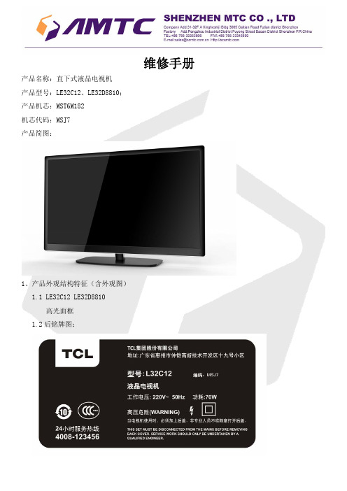
32" LE32C12 LE32D8810
MTC AU/SHARP/BOE
A 1366*768 MSTAR 6M182 左右上 24.91,下 39.65
4、使用者的警告 4.1 警告:
为了防止电击或火灾,请不要将电视放到有雨雾的场所。不要使用任何可能对显示屏造成刮 伤、毁坏的硬物体磨擦或敲击显示屏。 4.2 注意: 禁止在未经授权的情况下以任何方式私自更改本产品。 4.3 供电电源 产品直接用交流电供电,供电电压值见电视后盖标牌上的说明。将交流电源线一端按照电视 后端子标牌标注位置插入电源端口,另一端接在电源插座即可完成电源连接。 在有雷电或交 流供电断电的时候,请拔掉电源插头和天线插头。电源线不允许有任何其它东西帖靠或缠绕 在上面,也不要将电源线置于可能受到毁坏的地方。 4.4 使用场所 避免电视的屏幕直接对着外界的强光或阳光。避免电视受到不必要的任何振动,不要将电视 置于过湿、过热或多灰尘的地方。保证电视有良好的空气对流,不要将任何物体覆盖在后盖 的通风口上。 4.5 清洁 在清洁电视屏之前将电源插头拔下。使用干净的软布擦拭显示屏和电源线。如果显示屏需要 特别的清洗,请使用干净、潮湿的抹布进行擦拭。请不要使用任何汽油、酒精、苯类有机液 体或气雾状清洁剂。请不要用力过大以致损坏屏幕。 4.6 注意事项 显示屏属于精密显示器件,屏幕上有个别的亮点、暗点,或红、绿、蓝色之类的少许死像素 这是正常现象,不属于不良品。 A、显示屏长时间显示同一个静止画面时,会在电视上留下一 个残影,这种损坏属于使用不当造成的。 B、电视在连接各种系统时,可能会出现系统不匹 配的现象,特别是连接电脑时,有些显卡可能不匹配,而且本机只识别刷新率为 60HZ。 C、 由于本机使用嵌入式的操作系统,软件比较复杂,可能在工作中或待机中出现软件问题,如 果重新启动能恢复正常,就不属于故障。
TVR6000中文手册

步驟一、D/A1. D/A2 輸出電壓調整:........................................................36 步驟二、AD/DA 之輸入電壓調整.............................................................37 IF 校正 .................................................................................................................38 IF 電流源校正共分為四個步驟 : ..............................................................38 比對 IF 板 OP 放大器回路電壓是否正常 .................................................38 IF 電流檔位 2,RANGE 0.6A-25A 檔位校正 ...........................................39 IF 電流檔位 1,RANGE 0.01A ~0.5A 檔位校正.......................................40 VR Source 校正....................................................................................................41 基本功能檢查.............................................................................................. 41 效驗方式...................................................................................................... 42 VBR 校正............................................................................................................43 IR 校正................................................................................................................44 第七章、 光遮斷器與啟動訊號..........................................................................45 SOT 負源觸發 .....................................................................................................47 SOT 正源觸發: .................................................................................................48 第八章、 後面板說明..........................................................................................49 第九章、 測試機內視圖......................................................................................51
LCD12864(T6963)驱动程序

液晶显示模块的应用一、结构特点内藏T6963C 的液晶显示模块上已经实现了T6963C 与行、列驱动器及显示缓冲区RAM 的接口,同时也已用硬件设置了液晶屏的结构(单双屏、数据传输方式、显示窗口长度、宽度等等。
我们常用的液晶显示模块一般都是单屏结构,因此我们这里只讨论单屏结构的液晶显示模块。
内藏T6963C 的单屏结构点阵图形液晶显示模块的方框图如下:二、T6963C 的特点(1) T6963C 是点阵式液晶图形显示控制器它能直接与8 位微处理器接口;(2) T6963C 的字符字体可由硬件或软件设置,其字体有4 种5X8 、6X8 、7X8、8X8;(3) T6963C 的占空比可从1/16 到1/128;(4) T6963C 可以图形方式、文本方式及图形和文本合成方式进行显示,以及文本方式下的特征显示,还可以实现图形拷贝操作等等;(5) T6963C 具有内部字符发生器CGROM,共有128 个字符。
T6963C 可管理64K显示缓冲区及字符发生器CGRAM,并允许MPU 随时访问显示缓冲区,甚至可以进行位操作。
三、该类液晶模块的管脚定义见下表:说明:对于单电源模块,标志为V0/POFF。
当该管脚为高或悬空时,内部DC/DC 功能开启;为低时,内部DC/DC 功能关闭。
该功能可用作屏幕保护和休眠方式。
如果用其直接替代双电源模块,该管脚直接悬空即可。
四、液晶显示模块的供电说明1. 如果您所选用的液晶模块是双电源(VDD/V0)供电的就需要提供一个负电压(液晶驱动电压V0/VEE),用以调节对比度,接在液晶模块的V0 引脚上。
因为液晶材料的物理特性,液晶的对比度会随着温度的变化而相应变化,所以,您加的负电压值应该随温度作相应的调整,大致是温度变化10°C 电压变化1伏左右。
为满足这一要求您要选择较大值的负电源,然后做一个温度补偿电路,或者安排一个电位器调整负电压值。
例如对于QH12864T-HT-LED04,当室温(VDD=5V)时,V0=-10.5V,如果要用到-20°C,液晶驱动电压将要变到V0=-14.5V,再考虑到负载消耗所以您提供的负电源应该为-16V 左右。
T61系列驱动大全
T61系列驱动大全感谢您使用ThinkPad,下面是适用于您所购买产品的驱动程序,驱动下载页面的“驱动描述”中有关于驱动安装的详细说明,建议仔细阅读!几点提醒:1、请尽量按照下列驱动的排列的先后顺序安装;下载完的驱动程序文件是一个可执行文件,但是双击后仅是释放文件的过程,并未安装,默认释放到C:\\DRIVERS\\WIN\\***目录下,请到释放文件目录下继续安装。
2、设备管理中常见的未知设备一般为ACPI电源管理器,如果出现未知设备,请首先尝试安装其驱动。
3、GHOST安装的系统有可能存在驱动无法安装的情况,建议不要使用GHOST安装系统。
4、使用GHOST安装系统后如出现小红帽不可用的情况,请在设备管理器中删除“鼠标和其它指针设备”下面有感叹号的设备,然后重启系统,小红帽即可使用。
附:BIOS中更改硬盘模式方法:在安装Win XP之前,需要在BIOS中将硬盘改为兼容模式,否则在安装时会提升找不到硬盘或蓝屏, 修改方法为:开机屏幕上出现ThinkPad标志时按F1进入BIOS--> Config-->Select Serial ATA (SATA),把AHCI改为Compatibility后按F10保存退出即可。
驱动下载地址及安装路径:1、Intel主板驱动程序(Windows Vista/XP/2000)(设备管理器中显示为:SM总线控制器): /support/driver/detail.aspx?docID=DR1198033155359&docTypeID=D OC_TYPE_DRIVER默认解压路径:C:\\DRIVERS\\WIN\\INTELINF\\INFINST_AUTOL.EXE2、(NVIDIA Quadro NVS 140M / Quadro FX 570M)显卡驱动程序(Windows XP, 2000)(设备管理器中显示为:视频控制器):/support/driver/detail.aspx?docID=DR1197957391968&docTypeID=D OC_TYPE_DRIVER默认解压路径:C:\\DRIVERS\\WIN\\DISPLAY\\SETUP.EXE或C:\\DRIVERS\\WIN\\VIDEO\\SETUP.EXE3、以太网卡驱动程序(Windows 2000/XP)(设备管理器中显示为:以太网控制器):/support/driver/detail.aspx?docID=DR1197611181968&docTypeID=D OC_TYPE_DRIVER默认解压路径C:\\DRIVERS\\WIN\\ETHERNET\\APPS\\SETUP\\SETUPBD\\Win32\\SetupBD.exe或C:\\DRIVERS\\WIN\\ETHERNET\\APPS\\PROSETDX\\Win32\\DxSetup.EXE4、Intel PRO无线网卡驱动程序(Windows XP/2000)(设备管理器中显示为:网络控制器):/support/driver/detail.aspx?docID=DR1197856074093&docTypeID=D OC_TYPE_DRIVER默认释放路径C:\\DRIVERS\\WIN\\WLANINT2\\XP\\Apps\\x32\\iProInst.EXE5、声卡KB888111补丁(设备管理器中显示为:其他设备:PCI-DEVICE)(必须先安装此补丁,否则无法安装声卡和MODEM驱动程序)/support/knowledge/detail.aspx?docID=26015&docTypeID=DOC_TYP E_KNOWLEDGE默认释放路径:点击页面最下方附件文档下载,下载后是一个ZIP文件,先解压再安装即可。
Hitachi 存储 adapter 说明书

© 2016 Hitachi, Ltd. All rights reserved.RN-90ADPTR013-09 Apr 20161Hitachi Storage Adapter for Microsoft ® SQL Server Remote BLOB Storagev01.13.0 Release NotesContentsAbout this Document ........................................................................ 2 Intended Audience............................................................................ 2 Getting Help .................................................................................... 2 Hardware and Software Support ......................................................... 3 About This Release ........................................................................... 5 Changes in This Release .................................................................... 5 Known Problems .............................................................................. 5 Documentation ................................................................................ 6 Copyrights and Licenses .. (7)© 2016 Hitachi, Ltd. All rights reserved. RN-90ADPTR013-09 Apr 20162About this DocumentThis document provides the latest information about the Hitachi Storage Adapter for Microsoft SQL Server Remote BLOB Storage. It includes information that was not available at the time the technical documentation for this product was published, as well as a list of known problems and solutions.Intended AudienceThis document is intended for customers and Hitachi, Ltd. partners who license and use the Hitachi Storage Adapter for Microsoft SQL Server Remote Blob Storage.Getting HelpNo technical support license is required for Hitachi Content Platform (HCP).The Hitachi Data Systems Support Center staff is available 24 hours a day, seven days a week. Provisions for patches and fixes are restricted to normal business hours, 8 a.m. to 5 p.m. PST. If you need technical support, log on to the Hitachi Data Systems Portal contact information: https:// . If you purchased this product from an authorized Hitachi Data Systems reseller, contact that reseller for support.Before calling the Hitachi Data Systems Support Center, please provide as much information about the problem as possible, including:The circumstances surrounding the error or failure.The exact content of any error message(s) displayed on theHardware and Software SupportNote This release supports only the software and hardwarelisted below.Supported Software© 2016 Hitachi, Ltd. All rights reserved. RN-90ADPTR013-09 Apr 20163Supported Hardware© 2016 Hitachi, Ltd. All rights reserved. RN-90ADPTR013-09 Apr 20164© 2016 Hitachi, Ltd. All rights reserved. RN-90ADPTR013-09 Apr 20165About This ReleaseSee the new features in the following change list.Changes in This ReleaseNew FeaturesAdded support for new VSP Gx00 UnifiedAdded support for new VSP Fx00Added support for new HCP 7.2.0 GA version.Added support for new HNAS 12.6 GA version. Added support for HCP 7.1 Retention PolicyKnown ProblemsDocumentationRelated DocumentHitachi Storage Adapter for Microsoft® SQL Server Remote BLOBStorage User’s Guide (MK-90ADPTR012-07).© 2016 Hitachi, Ltd. All rights reserved. RN-90ADPTR013-09 Apr 20166Copyrights and Licenses© 2016 Hitachi, Ltd. All rights reserved. No part of this publication may be reproduced or transmitted in any form or by any means, electronic or mechanical, including photocopying and recording, or stored in a database or retrieval system for any purpose without the express written permission of Hitachi, Ltd.Hitachi, Ltd., reserves the right to make changes to this document at any time without notice and assumes no responsibility for its use. This document contains the most current information available at the time of publication. When new or revised information becomes available, this entire document will be updated and distributed to all registered users.Some of the features described in this document might not be currently available. Refer to the most recent product announcement for information about feature and product availability, or contact Hitachi Data Systems Corporation at https://.Notice: Hitachi, Ltd., products and services can be ordered only under theterms and conditions of the applicable Hitachi Data Systems Corporation agreements. The use of Hitachi, Ltd., products is governed by the terms of your agreements with Hitachi Data Systems Corporation.Hitachi is a registered trademark of Hitachi, Ltd., in the United States and other countries. Hitachi Data Systems is a registered trademark and service mark of Hitachi, Ltd., in the United States and other countries.Archivas, Essential NAS Platform, HiCommand, Hi-Track, ShadowImage, Tagmaserve, Tagmasoft, Tagmasolve, Tagmastore, TrueCopy, Universal Star Network, and Universal Storage Platform are registered trademarks of HitachiData Systems Corporation.AIX, AS/400, DB2, Domino, DS6000, DS8000, Enterprise Storage Server, ESCON, FICON, FlashCopy, IBM, Lotus, MVS, OS/390, RS6000, S/390, Systemz9, System z10, Tivoli, VM/ESA, z/OS, z9, z10, zSeries, z/VM, and z/VSE are registered trademarks or trademarks of International Business Machines Corporation.All other trademarks, service marks, and company names in this document or website are properties of their respective owners.Microsoft product screen shots are reprinted with permission from Microsoft Corporation.© 2016 Hitachi, Ltd. All rights reserved. RN-90ADPTR013-09 Apr 20167。
HX8250
( DOC No. HX8250-A01-DS )HX8250-A01960CH TFT LCD Source Driver with TCONVersion 01 January, 2008HX8250-A01960CH TFT LCD Source Driverwith TCONVersion 01January, 2008 1. General DescriptionHX8250-A01 is a 960-channel outputs source driver with TCON, OSD mixer, and 3-wire Serial Port Interface. It also supports 2-chip cascade mode to extend source channel to be 1920 channels.The interface follows digital 8-bit serial/24-bit parallel RGB, CCIR601 and CCIR656 input format. The TCON generates the 960x240, 1920x240, and 1920x480 resolution and provides horizontal and vertical control timing to source driver and gate driver. It also supports dithering feature, apply source driver with 6-bit DAC to perform 8-bit resolution 256 gray scales.The source driver receives 6-bit by 3 dots of digital display data per clock from TCON and generates corresponding 64-level gray scale voltage output. Since the output circuit of this source driver incorporates an operational amplifier with low power dissipation, and performs wide voltage supply range and small output deviation.Therefore, a high quality display with less crosstalk can be achieved.2. FeaturesTCONz Support display resolution 960x240, 1920x240, and 1920x480z Support digital 8-bit serial RGB, CCIR601, and CCIR656 input mode z Support digital 24-bit parallel RGB input modez Internal dithering 8-bit data to 6-bit data for Source Driver Circuitz Only support stripe types of panel groupz Operation frequency: 40 MHz maxz Support NTSC/PAL TV systemz OSD overlay supported in CCIR601and CCIR656 input modez Provide source and gate drivers control timingz Provide flip and mirror scan controlz Operation Voltage Level 2.7V to 3.6VSource Driverz960 channels output source driver for TFT LCD panelz Dynamic output range: 0.1 to VDD-0.1Vz Voltage deviation of outputs: ±20mVz Dot inversion driving schemez Right and left shift capabilityz LCD power: 6.5 to 13.5VOthersz COG package3. Block Diagram3.1 Whole chip block diagramTCONCLKD0[7:0]D1[7:0]D2[7:0]HSVSDENSPENASPDASPCKOSD_R, G, BOSD_ENOSD_CLKOSD_HSOSD_VSRESETBMASLIF[2:0]OSDDecoder3-WireDecoderGammaV1~V10SO[1:960]DD0[5:0]DD1[5:0]DD2[5:0]CKHSTHOEHRLSTBPOLCKVOEVSTVD/STVUUDBUDPPOLSourceDriverRESL[1:0]STBNPCFigure 3. 1 HX8250-A01 block diagram3.2 Source driver block diagramLine BufferSTHRL CKH Level ShifterD/A ConverterBufferDD00~DD05LatchPOL OEHV 1 ~ V10320-bit Bi-directional Shift Register666DD10~DD15DD20~DD25Figure 3. 2 Source driver block diagram4. Pin descriptionPin name I/O Description CLK I Clock signal. Latching data at the rising edge.D07~D00D17~D10 D27~D20IDigital data input. DX0 is LSB and DX7 is MSB.1. If parallel RGB input mode is used, D0X, D1X, and D2X indicate R, G, andB data in turn.2. If serial RGB or CCIR601 or CCIR656 input mode is selected, onlyD07~D00 are used, and others short to GND.When disable dithering function, please use DX07~DX02 as 6-bit input. HS IHorizontal sync input in digital RGB and CCIR601 mode.(Short to GND if not used)VS IVertical sync input in digital RGB and CCIR601 mode.(Short to GND if not used)DEN IInput data enable control. When DE mode, active High to enable data input.Default pull low.NPC O NTSC or PAL mode auto detection result.When NPC=H, NTSC mode is selected.When NPC=L, PAL mode is selected.RESETB I Hardware global reset. Low active. Default pull high.MASL IMaster and slave mode selection. Default pull high. Only used in cascade mode.MASL = “H”, for Master mode. MASL = “L”, for Slave mode.POL_I I Sync control input signal in cascade mode. Default pull low.When used as slave chip in cascade mode, receive the sync control signalfrom master chip. Please keep open when no use. POL_O OSync control output signal in cascade mode.When used as master chip in cascade mode, output sync control signal to next slave chip. POL_O will keep Hi-Z when no use.LRI The shift direction of device internal shift register is controlled by this pin as shown below:LR=H: STH ÆSO1Æ• • •ÆSO960ÆSTHO LR=L: STH ÆSO960Æ• • •ÆSO1ÆSTHO UDIUp/down scan setting. When UD=H, reverse scan.When UD=L, normal scan. IF[2:0] IControl the input data format.IF[2:0] Input data format 000 8-bit Serial RGB 001 (default) 24-bit Parallel RGB010 CCIR601 mode A 24.54MHz011 CCIR601 mode B 24.54MHz 100 CCIR601 mode A 27MHz 101 CCIR601 mode B 27MHz 110 CCIR656 mode A 27MHz 111 CCIR656 mode B 27MHzRESL[1:0] IControl the resolution selection.RESL[1:0] Resolution00 960x24001 1920x240 10 (default) 1920x480 (parallel RGB only)11 reservedFRP I Select normally white or normally black panel. Default pull low.FRP=L, pass the input data for normally white panel.FRP=H, inverse the input data for normally black panel. CS I Charge share function control. Default pull high.CS=L, disable charge share function.CS=H, enable charge share function. STB I Standby mode control. Default pull high.When STB=L, TCON and source driver are off.When STB=H, all the functions are on. V1~V10 I Used as reference voltage input pins.Hold the reference voltage fixed during the period of LCD drive output. Toensure the correct analog voltage is output from D/A converter, the V1~V10must be stable before D/A conversion.VDD>V1>V2>V3>V4>V5>V6>V7>V8>V9>V10>VSS.SPCK I Serial port Clock. Default pull high. SPDA I/O Serial port Data input/output. Default pull high. SPENA I Serial port Data Enable Signal. Default pull high. CKV O Gate driver clock. OEV O Enable output control of gate driver.STVD O Start pulse for gate driver.When UD=L, STVD is output.When UD=H, STVD is Hi-Z. STVU O Start pulse for gate driver.When UD=L, STVU is Hi-Z.When UD=H, STVU is output.UDB O Reverse of UD. UDP O Internal link to UD. OSD_HS O OSD Hsync output. OSD_VS O OSD Vsync output. OSD_CLK O OSD clock output. OSD_R I OSD red data input. Default pull low. OSD_G I OSD green data input. Default pull low. OSD_B I OSD blue data input. Default pull low.OSD_EN I OSD enable input. Default pull low.OSD_EN=H : OSD enable.OSD_EN=L : OSD disable.SO1~SO960 O Output driver signal. TEST1 I Test pins. Default pull low. TEST2 I Test pins. Default pull low. TP[7:0] O Test pins. They must be open. TESTO O Test pin. It must be open. VDD I Analog power. 6.5V to 13.5V. VSS I Analog ground. VCC I Digital power. 2.7V to 3.6V. GND I Digital ground. PASSR1PASSR2 - Link together internally. Please use as signal path, not power path.PASSL1PASSL2 - Link together internally. Please use as signal path, not power path.PASS1PASS2- Link together internally. Please use as signal path, not power path.Note: (1) Please power on following the sequence VCC Æ logic input Æ VDD and V1 ~ V10. Reverse thesequence to shut down.(2) To stabilize the supply voltages, please be sure to insert a 0.1uF bypass capacitor betweenVCC-GND and VDD-VSS. Furthermore, for increased precision of the D/A converter, insertion of abypass capacitor of about 0.01uF is also advised between the gamma-corrected power supplyterminals (V1, V2, …, V10) and VSS.(3) Please keep V1~V10 not cross to the toggle signals as possible to avoid the AC coupling on theDC V1~V10 voltage. When used as cascade mode, please keep the coupled amount of V1~V10are the same between the two chip.(4) The input wiring resistance values affect power or signal integrity and the display quality. So besure to design using values that do not exceed those recommended as below.Pin Name Wiring resistance value(Ω)VCC(3.3V) <3030GND(0V) <5 VDD(8.4V) <5 VSS(0V) <V1 ~ V10 < 100100 CLK < Dx7 ~ Dx0 < 200200 HS <200 VS <DE <200 POL_O to POL_I (cascade mode) < 200OSD_R, OSD_G, OSD_B< 200OSD_HS, OSD_VS, OSD_CLK1000 Others <5. Operation description5.1 Relationship between input data and output channelsz Source DriverLR First → Last H Out1 Out2 Out3 ••• ••• ••• ••• Out958 Out959 Out960LRLast← First L Out960 Out959Out958 ••••••••• ••• Out3 Out2 Out1Table 5. 1 Relationship between input data and output channels5.2 HX8250-A01 chip locations with LR and UD controlHX8250-A01 can be controlled Left/Right shift and Up/Down scan by LR and UD pins. The setting depends on HX8250-A01 and Gate Driver positions with panel. Please reference to below diagram to set the LR and UD.HX8250-A01HX 866019601240(1,240)(1,1)(960,1)(960,240)LR=1,UD=0OEV UDB STVD STVUHX8250-A01HX 866019601240(1,240)(1,1)(960,1)(960,240)LR=0,UD=0OEV UDB STVD STVUHX8250-A01HX 866019601240(1,240)(1,1)(960,1)(960,240)LR=1,UD=1OEV UDB STVD STVUHX8250-A01HX 866019601240(1,240)(1,1)(960,1)(960,240)LR=0,UD=1OEV UDB STVD STVU960(1,240)(1,1)(960,1)(960,240)LR=1,UD=0LR=0,UD=0LR=1,UD=1LR=0,UD=1HX8250-A01HX 866011240OEV UDP STVD STVU960(1,240)(1,1)(960,1)(960,240)HX8250-A01HX 866011240OEV UDP STVD STVU960(1,240)(1,1)(960,1)(960,240)HX8250-A01HX 866011240OEV UDP STVD STVU960(1,240)(1,1)(960,1)(960,240)HX8250-A01HX 866011240OEV UDP STVD STVUFigure 5. 2 HX8250-A01 chip put down side and Gate Driver put right side.LR=0,UD=1LR=1,UD=1LR=0,UD=0LR=1,UD=0HX8250-A01HX 866019601240OEV UDP STVD STVU (1,240)(1,1)(960,1)(960,240)HX8250-A01HX 866019601240OEVUDP STVD STVU (1,240)(1,1)(960,1)(960,240)HX8250-A01HX 866019601240OEV UDP STVD STVU (1,240)(1,1)(960,1)(960,240)HX8250-A01HX 866019601240OEVUDP STVD STVU (1,240)(1,1)(960,1)(960,240)LR=0,UD=1LR=1,UD=1LR=0,UD=0LR=1,UD=0(1,240)(1,1)(960,1)(960,240)2409601HX8250-A01HX 86601OEV UDB STVD STVU (1,240)(1,1)(960,1)(960,240)2409601HX8250-A01HX 86601OEV UDB STVD STVU (1,240)(1,1)(960,1)(960,240)2409601HX8250-A01HX 86601OEV UDB STVD STVU (1,240)(1,1)(960,1)(960,240)2409601HX8250-A01HX 86601OEV UDB STVD STVU Figure 5. 4 HX8250-A01 chip put up side and Gate Driver put Left side.5.3 Digital RGB data input formatFor digital RGB input data format, both SYNC mode and DE mode are supported. HX8250-A01 will auto detect which mode is used. If DEN signal is fixed low, SYNC mode is used. Otherwise, DE mode is used. The OSD function is not supported in digital serial/parallel RGB mode.5.4 NTSC/PAL mode auto detectionFor NTSC/PAL mode setting, the auto-detection function is implemented. You don’t have to define this setting and can use NPC pin to monitor detection result.5.5 Cascade mode for 1920x240, 1920x480 resolutionsHX8250-A01 supports 1920x240 and 1920x480 resolutions by cascade 2 chips. When connect to cascade mode, user need to set MASL pin to define which chip is master mode or slave mode. Master chip and slave chip are decided by the fixed position. Always master chip’s SO960 is neighbor to slave chip’s SO1.It needs to receive the polarity signal from the master chip for the polarity synchronized. chip and POL_O of Slave chip could keep NC. Please reference to the followingdiagrams.Signals to gate driver could be provided by master chip or slave chip. Each side of master chip or slave chip could provide the gate signals, and user can chooses thecloser side to connect with gate driver.Please minimize the parasitic R of the POL path. The parasitic R should be smaller than 200 ohm.GateDriver640RGBx480(640RGBx240)(1,1)(640, 1)(1,480)(640, 480)MASL=1MASL =0STVD,STVUOEV,UDB,CKV HX8250-A01HX8250-A01S 960S1S1 S960POL _OPOL _IPOL _IPOL _O(1,1)(640, 1)(1, 480)(640, 480)Gate DriverMASL=1MASL =0S 960S 1 S1 S 960POL _OPOL _IPOL _IPOL _OSTVD,STVUOEV,UDP,CKVLR=1,UD=0640RGBx480(640RGBx240)LR=1,UD=0HX8250-A01HX8250-A01Figure 5. 5 2-chip cascade for 1920x4805.6 Relationship between gamma correction and output voltageThe output voltage is determined by the 6-bit digital input data, and the V1 ~ V10 gamma correction reference voltage inputs.Gamma correction characteristic curve:00H08H10H18H20H28H30H38H3FHInput data VDD V1V2V3V4V5V6V9V10VSSV7V8Figure 5. 6 Gamma correction characteristic curveGamma correction resistor ratio: (1 unit = 125ohm) Name Resistor Name Resistor R0 6.4 R320.8 R1 6 R330.8 R2 5.6 R340.8 R3 5.2 R350.8 R4 4.8 R360.8 R5 4.4 R370.8 R6 4.4 R380.8 R7 4 R390.8 R8 4 R400.8 R9 3.2 R410.8 R10 3.2 R420.8 R11 2.8 R430.8 R12 2.8 R440.8 R13 2.8 R450.8 R14 2.4 R460.8 R15 2.4 R470.8R16 2.4 R480.8 R17 2 R490.8 R18 2 R500.8 R19 2 R510.8 R20 1.6 R520.8 R21 1.6 R53 1.2 R22 1.6 R54 1.2 R23 1.2 R55 1.2 R24 1.2 R56 1.6 R25 1.2 R57 1.6 R26 1.2 R58 2 R27 0.8 R59 2 R28 0.8 R60 2.4 R29 0.8 R61 4 R30 0.8 R62 6.4R31 0.8V1, V10V2, V9V3, V8 V4, V7 V5, V6Output Voltages vs. Source Input Data:Data Positive polarity Output Voltage Negative polarity Output Voltage V1 V1000H01H V2 + ( V1 – V2)X 58 / 64.4 V10 + ( V9 – V10)X 6.4 / 64.402H V2 + ( V1 – V2)X 52 / 64.4 V10 + ( V9 – V10)X 12.4 / 64.403H V2 + ( V1 – V2)X 46.4 / 64.4 V10 + ( V9 – V10)X 18 / 64.404H V2 + ( V1 – V2)X 41.2 / 64.4 V10 + ( V9 – V10)X 23.2 / 64.405H V2 + ( V1 – V2)X 36.4 / 64.4 V10 + ( V9 – V10)X 28 / 64.406H V2 + ( V1 – V2)X 32 / 64.4 V10 + ( V9 – V10)X 32.4 / 64.407H V2 + ( V1 – V2)X 27.6 / 64.4 V10 + ( V9 – V10)X 36.8 / 64.408H V2 + ( V1 – V2)X 23.6 / 64.4 V10 + ( V9 – V10)X 40.8 / 64.409H V2 + ( V1 – V2)X 19.6 / 64.4 V10 + ( V9 – V10)X 44.8 / 64.40AH V2 + ( V1 – V2)X 16.4 / 64.4 V10 + ( V9 – V10)X 48 / 64.40BH V2 + ( V1 – V2)X 13.2 / 64.4 V10 + ( V9 – V10)X 51.2 / 64.40CH V2 + ( V1 – V2)X 10.4 / 64.4 V10 + ( V9 – V10)X 54 / 64.40DH V2 + ( V1 – V2)X 7.6 / 64.4 V10 + ( V9 – V10)X 56.8 / 64.40EH V2 + ( V1 – V2)X 4.8 / 64.4 V10 + ( V9 – V10)X 59.6 / 64.40FH V2 + ( V1 – V2)X 2.4 / 64.4 V10 + ( V9 – V10)X 62 / 64.4V2 V910H11H V3 + (V2 – V3) X 19.6 / 22 V9 + ( V8 – V9)X 2.4 / 2212H V3 + (V2 – V3) X 17.6 / 22 V9 + ( V8 – V9)X 4.4 / 2213H V3 + (V2 – V3) X 15.6 / 22 V9 + ( V8 – V9)X 6.4 / 2214H V3 + (V2 – V3) X 13.6 / 22 V9 + ( V8 – V9)X 8.4 / 2215H V3 + (V2 – V3) X 12 / 22 V9 + ( V8 – V9)X 10 / 2216H V3 + (V2 – V3) X 10.4 / 22 V9 + ( V8 – V9)X 11.6 / 2217H V3 + (V2 – V3) X 8.8 / 22 V9 + ( V8 – V9)X 13.2 / 2218H V3 + (V2 – V3) X 7.6 / 22 V9 + ( V8 – V9)X 14.4 / 2219H V3 + (V2 – V3) X 6.4 / 22 V9 + ( V8 – V9)X 15.6 / 221AH V3 + (V2 – V3) X 5.2 / 22 V9 + ( V8 – V9)X 16.8 / 221BH V3 + (V2 – V3) X 4 / 22 V9 + ( V8 – V9)X 18 / 221CH V3 + (V2 – V3) X 3.2 / 22 V9 + ( V8 – V9)X 18.8 / 221DH V3 + (V2 – V3) X 2.4 / 22 V9 + ( V8 – V9)X 19.6 / 221EH V3 + (V2 – V3) X 1.6 / 22 V9 + ( V8 – V9)X 20.4 / 221FH V3 + (V2 – V3) X 0.8 / 22 V9 + ( V8 – V9)X 21.2 / 22Output Voltages vs. Source Input Data (continued):Data Positive polarity Output Voltage Negative polarity Output Voltage20H V3 V821H V4 + (V3 – V4) X 12 / 12.8 V8 + ( V7 – V8) X 0.8 / 12.822H V4 + (V3 – V4) X 11.2 / 12.8 V8 + ( V7 – V8) X 1.6 / 12.823H V4 + (V3 – V4) X 10.4 / 12.8 V8 + ( V7 – V8) X 2.4 / 12.824H V4 + (V3 – V4) X 9.6 / 12.8 V8 + ( V7 – V8) X 3.2 / 12.825H V4 + (V3 – V4) X 8.8 / 12.8 V8 + ( V7 – V8) X 4 / 12.826H V4 + (V3 – V4) X 8 / 12.8 V8 + ( V7 – V8) X 4.8 / 12.827H V4 + (V3 – V4) X 7.2 / 12.8 V8 + ( V7 – V8) X 5.6 / 12.828H V4 + (V3 – V4) X 6.4 / 12.8 V8 + ( V7 – V8) X 6.4 / 12.829H V4 + (V3 – V4) X 5.6 / 12.8 V8 + ( V7 – V8) X 7.2 / 12.82AH V4 + (V3 – V4) X 4.8 / 12.8 V8 + ( V7 – V8) X 8 / 12.82BH V4 + (V3 – V4) X 4 / 12.8 V8 + ( V7 – V8) X 8.8 / 12.82CH V4 + (V3 – V4) X 3.2 / 12.8 V8 + ( V7 – V8) X 9.6 / 12.82DH V4 + (V3 – V4) X 2.4 / 12.8 V8 + ( V7 – V8) X 10.4 / 12.82EH V4 + (V3 – V4) X 1.6 / 12.8 V8 + ( V7 – V8) X 11.2 / 12.82FH V4 + (V3 – V4) X 0.8 / 12.8 V8 + ( V7 – V8) X 12 / 12.830H V4 V731H V5 + (V4 – V5) X 26.8 / 27.6 V7 + ( V6 – V7) X 0.8 / 27.632H V5 + (V4 – V5) X 26 / 27.6 V7 + ( V6 – V7) X 1.6 / 27.633H V5 + (V4 – V5) X 25.2 / 27.6 V7 + ( V6 – V7) X 2.4 / 27.634H V5 + (V4 – V5) X 24.4 / 27.6 V7 + ( V6 – V7) X 3.2 / 27.635H V5 + (V4 – V5) X 23.6 / 27.6 V7 + ( V6 – V7) X 4 / 27.636H V5 + (V4 – V5) X 22.4 / 27.6 V7 + ( V6 – V7) X 5.2 / 27.637H V5 + (V4 – V5) X 21.2 / 27.6 V7 + ( V6 – V7) X 6.4 / 27.638H V5 + (V4 – V5) X 20 / 27.6 V7 + ( V6 – V7) X 7.6 / 27.639H V5 + (V4 – V5) X 18.4 / 27.6 V7 + ( V6 – V7) X 9.2 / 27.63AH V5 + (V4 – V5) X 16.8 / 27.6 V7 + ( V6 – V7) X 10.8 / 27.63BH V5 + (V4 – V5) X 14.8 / 27.6 V7 + ( V6 – V7) X 12.8 / 27.63CH V5 + (V4 – V5) X 12.8 / 27.6 V7 + ( V6 – V7) X 14.8 / 27.63DH V5 + (V4 – V5) X 10.4 / 27.6 V7 + ( V6 – V7) X 17.2 / 27.63EH V5 + (V4 – V5) X 6.4 / 27.6 V7 + ( V6 – V7) X 21.2 / 27.63FH V5 V65.7 SPI Register Description Address A0A1A2A3D0D1D2D3D4D5D6D7DataR0Register Name R1R2R3R4R50000100001001100001011STVP0FRAD1FRAD0CS DISP_ONA_TIME1B_TIME2B_TIME1STHD4STHD3STHD2STHD1STHD0AUTO_DPPSC STB RESETBRESL1RESL0IF2IF1IF0STHD5STVP3STVP2STVP1FRP FRC LPF VS_POLHS_POLNPC_SETNPC_INA_TIME0B_TIME0Test RW 00000000010100000100110001000001100011RW must always keep low. “ ”= don`t care.z Register R0Bit D7 D6 D5 D4 D3 D2 D1 D0 Name reserved reserved reserved reserved reserved PSC STB RESETB Default - - - - - 0 0 1Table 5. 2 Register R0 settingPSC: Operating mode setting by input pin or SPI register. PSC=“L”, set STB, FRP , CS, IF[2:0], RESL[1:0] by input pin. PSC=“H”, set STB, FRP , CS, IF[2:0], RESL[1:0] by SPI register.STB: Standby mode setting.STB=”L”, TCON and source driver are off.STB=”H”, all the functions are on.RESETB: Global reset.RESETB=”L”, global reset the whole chip. RESETB=”H”, Normal operation.z Register R1Bit D7 D6 D5 D4 D3 D2 D1 D0Name reserved reserved reserved RESL1RESL0IF2 IF1 IF0 Default 1 0 0 0 1Table 5. 3 Register R1 settingRESL [1:0]: Display resolution selection.RESL1 RESL0 Resolution0 0 960x2400 1 1920x2401 0 1920x480 (parallel RGB only)1 1 reservedTable 5. 4 Display resolution selection.IF [2:0]: Data input mode selection.IF2 IF1 IF0 Data input format Operating freq0 0 0 8-bit serial RGB 38.4MHz (Max)0 0 1 24-bit parallel RGB 25.175MHz (Max)0 1 0 CCIR601 (YUV mode A) 24.54MHz0 1 1 CCIR601 (YUV mode B) 24.54MHz1 0 0 CCIR601 (YUV mode A) 27MHz1 0 1 CCIR601 (YUV mode B) 27MHz1 1 0 CCIR656 (YUV mode A) 27MHz1 1 1 CCIR656 (YUV mode B) 27MHzTable 5. 5 Data input mode selection.z Register R2Bit D7 D6 D5 D4 D3 D2 D1 D0Name reserved reserved STHD5STHD4STHD3STHD2STHD1 STHD0 Default 0 0 0 0 0 0Table 5. 6 Register R2 settingSTHD [5:0]: adjust start pulse position by dotSTHD5 STHD4STHD3 STHD2STHD1STHD0STH positionadjustUnit0 0 0 0 0 0 0 T CPH 0 0 0 0 0 1 +1 T CPH 0 0 0 0 1 0 +2 T CPH 0 0 0 0 1 1 +3 T CPH 0 0 0 1 0 0 +4 T CPH 0 0 0 1 0 1 +5 T CPH 0 0 0 1 1 0 +6 T CPH 0 0 0 1 1 1 +7 T CPH 0 1 1 0 0 0 +24 T CPH 0 1 1 0 0 1 +25 T CPH 0 1 1 0 1 0 +26 T CPH 0 1 1 0 1 1 +27 T CPH 0 1 1 1 0 0 +28 T CPH 0 1 1 1 0 1 +29 T CPH 0 1 1 1 1 0 +30 T CPH0 1 1 1 1 1 +31 T CPH1 0 0 0 0 0 -1 T CPH 1 0 0 0 0 1 -2 T CPH 1 0 0 0 1 0 -3 T CPH 1 0 0 0 1 1 -4 T CPH 1 0 0 1 0 0 -5 T CPH 1 0 0 1 0 1 -6 T CPH 1 0 0 1 1 0 -7 T CPH 1 0 0 1 1 1 -8 T CPH 1 1 1 0 0 0 -25 T CPH 1 1 1 0 0 1 -26 T CPH 1 1 1 0 1 0 -27 T CPH 1 1 1 0 1 1 -28 T CPH 1 1 1 1 0 0 -29 T CPH 1 1 1 1 0 1 -30 T CPH 1 1 1 1 1 0 -31 T CPH 1 1 1 1 1 1 -32 T CPHTable 5. 7 Adjust start pulse position by dotz Register R3Bit D7 D6 D5 D4 D3 D2 D1 D0Name reserved reserved STVP3STVP2STVP1 STVP0 FRAD1 FRAD0 Default 0 0 0 0 0 0Table 5. 8 Register R3 settingSTVP [3:0]: adjust first line position by lineSTVP3 STVP2 STVP1 STVP0 STV position adjust Unit0 0 0 0 0 T H0 0 0 1 +1 T H0 0 1 0 +2 T H0 0 1 1 +3 T H0 1 0 0 +4 T H0 1 0 1 +5 T H0 1 1 0 +6 T H0 1 1 1 +7 T H1 0 0 0 -1 T H1 0 0 1 -2 T H1 0 1 0 -3 T H1 0 1 1 -4 T H1 1 0 0 -5 T H1 1 0 1 -6 T H1 1 1 0 -7 T H1 1 1 1 -8 T HTable 5. 9 Adjust first line position by lineFRAD [1:0]: Odd frame or Even frame advance control.FRAD1 FRAD0 Advance Frame Notes0 0 Default Odd/Even frame Tstv are the same0 1 Odd frame Even frame Tstv = STVP setting + 1H1 0 Even frame Odd frame Tstv = STVP setting + 1H1 1 Reserve ReserveNote: Please set the FRAD[1:0]=01 when CCIR601 NTSC/PAL¡B CCIR656 PAL mode¡F set the PRAD[1:0]=00 when CCIR656 NTSC mode for video decoder SAA7114¡C(Please refer the inputtiming of the “8.1.3 Data input format for CCIR601 Mode”)Table 5. 10 Odd frame or Even frame advance controlz Register R4Bit D7 D6 D5 D4 D3 D2 D1 D0NPC_INNPC_SET Name CS FRP FRC LPF VS_POL HS_POL1 0 1 1 0 0 0 1 DefaultTable 5. 11 Register R4 settingCS: Charge share function control.CS=L, disable charge share function.CS=H, enable charge share function.FRP: Select normally white or normally black panel.FRP=L, pass the input data for normally white panel.FRP=H, inverse the input data for normally black panel.FRC: Dithering ON/OFF control.FRC=L, Dithering function disable.FRC=H, Dithering function enableLPF: Low pass filter function enable/disable in CCIR656/CCIR601 modeLPF=”L”, Low pass filer function disableLPF=”H”, Low pass filer function enableVS_POL: VS polarity setting.VS_POL=L, negative polarity.VS_POL=H, positive polarity.Note: Please set the VS_POL=H when CCIR601 mode for video decoder SAA7114.(Please refer the input timing of the “8.1.3 Data input format for CCIR601 Mode”)HS_POL: HS polarity setting.HS_POL=L, negative polarity.HS_POL=H, positive polarity.NPC_SET: Set the NTSC/PAL auto detection or define by NPC_IN.NPC_SET=L, auto detection.NPC_SET=H, define by NPC_IN.NPC_IN: Define the NTSC/PAL mode by SPI.NPC_IN=L, PAL.NPC_IN=H, NTSC.z Register R5Bit D7 D6 D5 D4 D3 D2 D1 D0 Name AUTO_DP DISP_ON A_TIME1A_TIME0B_TIME2B_TIME1 B_TIME0 reserved Default1 0 0 1 0 1 0Table 5. 12 Register R5 settingAUTO_DP: When power on, select blank image display time decided by A_TIME (bit 5, 4) or DISP_ON (bit 6).AUTO_DP =”L”, Blank image display time decided by DISP_ON (bit 6).AUTO_DP =”H”, Blank image display time decided by A_TIME(bit 5, 4). DISP_ON: When AUTO_DP (bit 7) = ”L”, and DISP_ON = ”H”, blank image display off, then display normal image.A_TIME [1:0]: When AUTO_DP(bit 7) = ”H”, the blank image display time is decided by A_TIME00: blank image display time is 8 VS time.01: blank image display time is 16 VS time.10: blank image display time is 32 VS time.11: blank image display time is 64 VS time.B_TIME [2:0]: When into STB mode, the blank image display time is decided by B_TIME.000: blank image display time is 3 VS time.001: blank image display time is 4 VS time.010: blank image display time is 5 VS time.011: blank image display time is 6 VS time.100: blank image display time is 7 VS time.101: blank image display time is 8 VS time.110: blank image display time is 9 VS time.111: blank image display time is 10 VS time.5.8 Power ON/OFF sequenceTo prevent the device damage from latch up, the power ON/OFF sequence shown below must be followed.Power ON: VCC, GND Æ VDD, VSS Æ V1 to V10Power OFF: V1 to V10 Æ VDD, VSS Æ VCC, GNDHX8250-A01 has a power ON sequence control function. There are two kinds of the mode. One is auto mode, and another is manual mode.Auto Mode: When power is ON, blank data is outputted for 16-frames (default value) first, from the falling edge of the following VS signal. The blank data would be gray level 255 for normally white panel.It can be defined in register R5 A_TIME1(bit 5) and A_TIME0(bit 4) whenAUTO_DP(bit 7) = ”H”RESETBVSSourceOutput invalid valid114151617VCCBlank dataSTBFigure 5. 7 Power on control for Auto ModeManual Mode: When power is ON, you should set the register R5 AUTO_DP(bit 7) = ”L” to stay at the manual mode. Blank data is outputted until the DISP_ON(bit 6) = H then display the normal image.5.10 Standby ON/OFF ControlHX8250-A01 has a standby ON/OFF sequence control function. When STB pin is “L”, blank data is outputted for 5-frames (default value) first, from the falling edge of the following VSYNC signal. The blank data would be gray level 255 for normally white panel. It can be defined in register R5 B_TIME[2:0] to adjust the frame number of the blank data.Figure 5. 9 Standby ON/OFF Control5.11 Reset when power onHX8250-A01 is internally initialized by the global reset signal, RESETB. The reset input must be held for at least 1ms after power is stable.TT>1ms90%VCCVDDRESETBFigure 5. 10 RESETB control after power stable6.1 Absolute Maximum Rating (GND=VSS=0V)Spec.Parameter SymbolMin. Typ. Max.UnitPower supply voltage 1 VCC -0.3 - +7.0 VPower supply voltage 2 VDD -0.3 - +13.5 VLogic Output Voltage V OUT -0.3 - +7.0 V Input voltage Vin -0.3 - VDD+0.3 V Operation temperature T OPR -40 - +85Storage temperature T STG -55 - +125Note: (1)All of the voltages listed above are with respective to GND=VSS=0V.(2)Device is subject to be damaged permanently if stresses beyond those absolute maximum ratings listed above.6.2 DC Electrical Characteristics (GND=VSS=0V, TA=25)Spec.Parameter SymbolMin. Typ. Max.Unit ConditionPower supply voltage VCC 2.7 3.3 3.6 V -Power supply voltage VDD 6.5 8.4 13.5 V -Low level input voltage V IL0-0.3VCC V-High level input voltage V IH0.7VCC-VCC V-Output low voltage V OL0-0.2VCC V I OL=400µAOutput high voltage V OH0.8VCC-VCC V I OH=-400µAInput leakage current I IN-1-+1µA No pull up or pull down.Output voltage deviation V VD - ±20 - mVSO1~SO960,V IN=0.1~13.4V,DC offset V OS - - ±20mV SO1~SO960, V IN=0.1~13.4V,Output leakage current I O -1 - +1µA SO1~SO960 at high impedancePull high resistance R H 600 900 1200 kΩRESETB,STB, MASL, CS, SPCK, SPENA, SPDA, RESL1, IF0Pull low resistance R L 600 900 1200kΩDEN,IF[2:1],RESL0, FRP, Dx[7:0], OSD_EN,OSD_R,OSD_G,OSD_B, TEST1, TEST2Output current I OH 40 60 - µA SO1~SO960,V O =9.9V vs. 9V, VDD=10VOutput current I OL 40 60 - µA SO1~SO960,Vo=0.1V vs. 1.0V, VDD=10VAnalog operating current I DD - 6 - mAF cph =19.2MHz, serial RGB,f HS=15.7KHz, black pattern,VDD=8.4V, RL=2K,CL=60pFDigital operating current I CC- 2.5 - mA F cph =19.2MHz, serial RGB, f HS=15.7KHz, black pattern, VCC=3.3VAnalog standby current I VDD- - 10 µA All LCD outputs are High-Z.Digital standby current I VCC - - 10 µA All inputs are stopped and outputs are High-Z.。
联想 L196wD显示器 说明书
⫼᠋ݠ
© Copyright Lenovo 2008.
iii
本《用户指南》包含有关您的平板监视器的详细信息。要快速获得一个总体认识, 请参阅监视器随附的“安装海报”。
产品包应该包含以下物品: ·安装海报 ·保证卡 · · ·电源线 · ·USB数据线
8 *E/`SwD<q,40T/<qhC1|#T/<qhCh*`Sw$HAY 15 VS##fYwP;h*C=h#
":g{T/<qhC;Ph(zh*D<q,k4PV/<qhC#kNDZ 3-3 3D:V/<qhC;#
Z 1 B kE 1-5
Z 2 B w{M9C`Sw
>Z+rza)PXw{M9C`SwDE"#
њ㾷⬉⑤ㅵ⧚
当计算机识别出您在用户限定的时间段内未使用鼠标或键盘时调用电源管理。有下表所描 述的几种状态。
要获取最佳性能,每天工作结束时或者一天中当您准备离开且长时间不能使用监视器时, 请关闭监视器。
߄!/!!䰃ྍࡰҢ㝜 状态
开启 待机/暂挂
关闭
电源指示灯 稳定的绿色 稳定的淡黄色
熄灭
屏幕 正常 黑屏
p5# v 9C,92gd=r`FmSADNNe`A#bI\aK&A;xrD2Gc#
k: v C.Tr*;iamD<"C|4aaXACbGMA;# v CI<MT"BMDe`AA%M,r8F#
pk`Sw'\
压 上的卡钩
如图所示, 略压束线夹两侧, 将其取下; 向后按后盖凹槽, 取下支撑臂后盖; 拧下四颗螺丝; 取下整个支撑臂, 显示器即可挂于壁上.
图像设定 色温调整
内存错误代码大全
系统内存蓝屏的错误代码大全系统内存蓝屏的错误代码大全0 0x00000000 作業完成。
1 0x00000001 不正确的函數。
2 0x00000002 系統找不到指定的檔案。
3 0x00000003 系統找不到指定的路徑。
4 0x00000004 系統無法開啓檔案。
5 0x00000005 拒絕存取。
6 0x00000006 無效的代碼。
7 0x00000007 儲存體控制區塊已毀。
8 0x00000008 儲存體空間不足,無法處理這個指令。
9 0x00000009 儲存體控制區塊地址無效。
10 0x0000000A 環境不正确。
11 0x0000000B 嘗試加載一個格式錯誤的程序。
12 0x0000000C 存取碼錯誤。
13 0x0000000D 資料錯誤。
14 0x0000000E 儲存體空間不夠,無法完成這項作業。
15 0x0000000F 系統找不到指定的磁盤驅動器。
16 0x00000010 無法移除目錄。
16 0x00000010 無法移除目錄。
17 0x00000011 系統無法将檔案移到其它的磁盤驅動器。
18 0x00000012 沒有任何檔案。
19 0x00000013 儲存媒體爲寫保護狀态。
20 0x00000014 系統找不到指定的裝置。
21 0x00000015 裝置尚未就緒。
22 0x00000016 裝置無法識别指令。
23 0x00000017 資料錯誤 (cyclic redundancy check)24 0x00000018 程序發出一個長度錯誤的指令。
25 0x00000019 磁盤驅動器在磁盤找不到持定的扇區或磁道。
26 0x0000001A 指定的磁盤或磁盤無法存取。
27 0x0000001B 磁盤驅動器找不到要求的扇區。
28 0x0000001C 打印機沒有紙。
29 0x0000001D 系統無法将資料寫入指定的磁盤驅動器。
30 0x0000001E 系統無法讀取指定的裝置。
映泰A770L3主板 BIOS说明书
3.1
跳线安装 ...........................................................................................12
3.2
安装细节 ...........................................................................................12
第五章: 帮助信息 ......................................................... 19
5.1
驱动程序安装注意事项 ...................................................................19
1.2 附件
HDD 数据线 X 1(可选) Serial ATA 数据线 X 2 ATX 机箱后置 I/O 面板 X 1 用户手册 X 1 驱动光盘 X 1 Serial ATA 电源线 X 1(可选) FDD 数据线 X 1 (可选) USB 2.0 数据线 X1 (可选)
x1
支持 PCI-E Gen2 x16 扩展卡
插槽
PCI Express Gen2 x1 插槽
x1
支持 PCI-E Gen2 x1 扩展卡
PCI 插槽
x3
支持 PCI 扩展卡
板载接口
软驱接口 打印机接口 IDE接口
x1
每个接口支持2个软驱
x1
每个接口支持1个打印机端口
x1
每个接口支持2个IDE设备
SATA 接口
x4
每个接口支持1个SATA设备
IBM安装WinXP详细教程
T61/R61/X61安装WinXP详细教程ThinkPad T61/R61/X61系列硬件架构相当接近,原厂维修手册都可共享,此篇安装流程理论上可以适用在 ThinkPad T61/R61/X61系列上面,记得再根据个别机种的硬件安装对应驱动程序。
ThinkPad 全系列机型驱动程序矩阵列表由于微软的许多组件都需在线下载,无法直接下载完整版本,因此才会视需要,将网络卡的驱动程序安装程序放在前面。
此外 ThinkPad 的相关驱动程序也有安装顺序上的考虑,以下的安装流程其实已经把各环节都尽量考虑进去,如网友没有把握,不妨按照以下的顺序安装,感谢。
准备动作、设定 SATA 硬盘自从 T60/R60/X60 开始改用 SATA 界面硬盘,手动安装 WinXP 便遇到一个问题:「要选择Compatibility 还是 AHCI 模式?」,这问题的主因源自于设定为 AHCI 模式时,必须在安装时按下「 F6 」,然后预先加载芯片组驱动程序。
但现在拥有 USB 界面软驱的使用者实在太少了。
在没有 USB 软驱的状况下,有的使用者便设定成「 Compatibility 模式」,却发现硬盘效能不彰,接着去 BIOS 调回 AHCI 模式之后,就会发生蓝底白字的系统当机惨剧。
因此很多人想到要重装 WinXP 就头大。
但根据 Lenovo 原厂提供的资料,以及亲身体验,其实手动安装 WinXP 并不困难!不需要准备 USB 软驱﹔不用忍受「 Compatibility 模式」效能不彰问题,更不会发生蓝底白字惨剧,关键只在于「安装流程的顺序!」请跟着本文的流程依序安装,相信大家都能顺利重返 WinXP 环境!1. 按下电源开关,开机时请按「 F1 」键,之后会进入 BIOS 画面。
2. 进入 BIOS 之后,进入「 Config 」页面3. 再进入「 Serial ATA(SATA) 」页面4. 将原先的「 AHCI 」改成「 Compatibility 」换言之,手动安装 WinXP 时,先采用「 Compatibility 模式」,规避掉需要透过 USB 软驱安装驱动程序的困扰,然后在后面的「步骤三」请网友务必按照说明安装 Intel Matrix Storage Manager Driver ,同时将硬盘更改为 AHCI 模式。
- 1、下载文档前请自行甄别文档内容的完整性,平台不提供额外的编辑、内容补充、找答案等附加服务。
- 2、"仅部分预览"的文档,不可在线预览部分如存在完整性等问题,可反馈申请退款(可完整预览的文档不适用该条件!)。
- 3、如文档侵犯您的权益,请联系客服反馈,我们会尽快为您处理(人工客服工作时间:9:00-18:30)。
Powered by ICminer.com Electronic-Library Service CopyRight 2003
Powered by ICminer.com Electronic-Library Service CopyRight 2003
Powered by ICminer.com Electronic-Library Service CopyRight 2003
Powered by ICminer.com Electronic-Library Service CopyRight 2003
Powered by ICminer.com Electronic-Library Service CopyRight 2003
Powered by ICminer.com Electronic-Library Service CopyRight 2003
Powered by ICminer.com Electronic-Library Service CopyRight 2003
Powered by ICminer.com Electronic-Library Service CopyRight 2003
Powered by ICminer.com Electronic-Library Service CopyRight 2003
Powered by ICminer.com Electronic-Library Service CopyRight 2003
Powered by ICminer.com Electronic-Library Service CopyRight 2003
Powered by ICminer.com Electronic-Library Service CopyRight 2003
Powered by ICminer.com Electronic-Library Service CopyRight 2003
Powered by ICminer.com Electronic-Library Service CopyRight 2003
Powered by ICminer.com Electronic-Library Service CopyRight 2003
Powered by ICminer.com Electronic-Library Service CopyRight 2003
Powered by ICminer.com Electronic-Library Service CopyRight 2003
Powered by ICminer.com Electronic-Library Service CopyRight 2003
Powered by ICminer.com Electronic-Library Service CopyRight 2003
Powered by ICminer.com Electronic-Library Service CopyRight 2003
Powered by ICminer.com Electronic-Library Service CopyRight 2003
Powered by ICminer.com Electronic-Library Service CopyRight 2003
Powered by ICminer.com Electronic-Library Service CopyRight 2003
Powered by ICminer.com Electronic-Library Service CopyRight 2003
Powered by ICminer.com Electronic-Library Service CopyRight 2003
Powered by ICminer.com Electronic-Library Service CopyRight 2003
Powered by ICminer.com Electronic-Library Service CopyRight 2003
Powered by ICminer.com Electronic-Library Service CopyRight 2003
Powered by ICminer.com Electronic-Library Service CopyRight 2003
Powered by ICminer.com Electronic-Library Service CopyRight 2003
Powered by ICminer.com Electronic-Library Service CopyRight 2003
Powered by ICminer.com Electronic-Library Service CopyRight 2003
Powered by ICminer.com Electronic-Library Service CopyRight 2003
Powered by ICminer.com Electronic-Library Service CopyRight 2003
Powered by ICminer.com Electronic-Library Service CopyRight 2003
Powered by ICminer.com Electronic-Library Service CopyRight 2003
Powered by ICminer.com Electronic-Library Service CopyRight 2003
Powered by ICminer.com Electronic-Library Service CopyRight 2003
Powered by ICminer.com Electronic-Library Service CopyRight 2003
Powered by ICminer.com Electronic-Library Service CopyRight 2003
Powered by ICminer.com Electronic-Library Service CopyRight 2003
Powered by ICminer.com Electronic-Library Service CopyRight 2003
Powered by ICminer.com Electronic-Library Service CopyRight 2003
Powered by ICminer.com Electronic-Library Service CopyRight 2003
Powered by ICminer.com Electronic-Library Service CopyRight 2003
Powered by ICminer.com Electronic-Library Service CopyRight 2003
Powered by ICminer.com Electronic-Library Service CopyRight 2003
Powered by ICminer.com Electronic-Library Service CopyRight 2003
Powered by ICminer.com Electronic-Library Service CopyRight 2003
Powered by ICminer.com Electronic-Library Service CopyRight 2003
Powered by ICminer.com Electronic-Library Service CopyRight 2003
Powered by ICminer.com Electronic-Library Service CopyRight 2003
Powered by ICminer.com Electronic-Library Service CopyRight 2003
Powered by ICminer.com Electronic-Library Service CopyRight 2003
Powered by ICminer.com Electronic-Library Service CopyRight 2003
Powered by ICminer.com Electronic-Library Service CopyRight 2003
Powered by ICminer.com Electronic-Library Service CopyRight 2003
Powered by ICminer.com Electronic-Library Service CopyRight 2003
Powered by ICminer.com Electronic-Library Service CopyRight 2003
Powered by ICminer.com Electronic-Library Service CopyRight 2003