UMC Design Rules
02-Transistors and Layout
11
Transistor structure
N-type transistor:
12
Simple Cross Section
SiO2
metal3
metal2
transistor poly n+ p+
metal1
via
n+ substrate substrate
13
Photolithography
28
Metal Migration
Current-carrying capacity of metal wire depends on cross-section Height is fixed, so width determines current limit Metal migration: when current is too high, electron flow pushes around metal grains. Higher resistance increases metal migration, leading to destruction of wire
gate oxide
silicide
source/ drain
poly
19
Fabrication Services
Educational services:
MOSIS (US):
/
EuroPractice (Europe):
Vgs = 2V:
Id
= 0.5k’(W/L)(Vgs-Vt)2= 93 A
Vgs = 5V:
Id
= 1 mA
IC模拟版图设计
1. 必要文件 2. 设计规则 DRC文件 4. LVS文件
整理ppt
39
第三部分:版图的准备
1. 必要文件
✓ PDK
✓ *.tf ✓ display.drf
✓ DRC ✓ LVS ✓ cds.lib ✓ .cdsenv ✓ .cdsinit
整理ppt
40
版图设计基础——设计规则
2)它需要设计者具有电路系统原理与工艺制造方面的基 本知识,设计出一套符合设计规则的“正确”版图也 许并不困难,但是设计出最大程度体现高性能、低功 耗、低成本、能实际可靠工作的芯片版图缺不是一朝 一夕能学会的本事。
第一部分:了解版图
3. 版图的工具:
– Cadence
✓ Virtuoso ✓ Dracula ✓ Assura ✓ Diva
MOS管剖面图
第二部分:版图设计基础
2.1 器件
2.1.1 MOS管
NMOS工艺层立体图
整理ppt
NMOS版图
13
第二部分:版图设计基础
2.1 器件
2.1.1 MOS管 1) NMOS管
✓ 以TSMC,CMOS,N单阱工艺 为例
✓ NMOS管,做在P衬底上,沟道 为P型,源漏为N型
2) 包括层次:
2) 选择用命令界面运 行LVS,定义查看 LVS报告文件及LVS 报错个数。
第三部分:版图的准备
定义金 属层数
关闭ERC 检查
用命令跑 LVS的方式
LVS COMPARE CASE NAMES
SOURCE CASE YES LAYOUT CASE YES
4. LVS文件
第三部分:版图的准备
4.4 layer mapping:
UMC2NT1资料
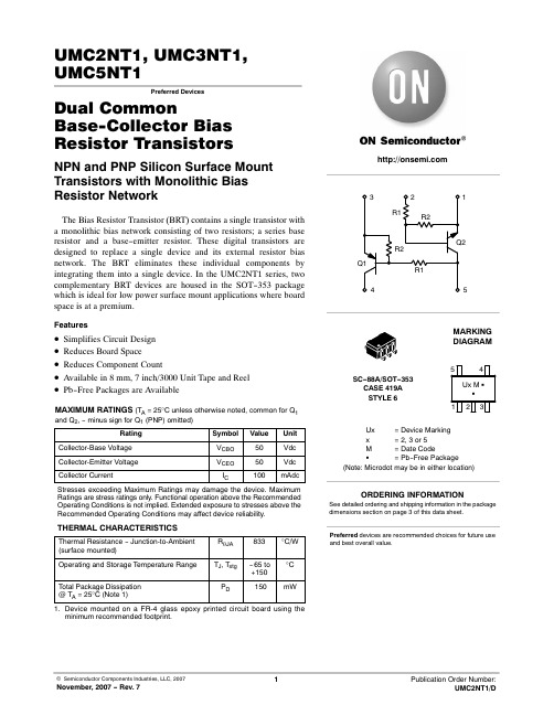
UMC2NT1, UMC3NT1,UMC5NT1Preferred DevicesDual CommonBase-Collector Bias Resistor TransistorsNPN and PNP Silicon Surface Mount Transistors with Monolithic BiasResistor NetworkThe Bias Resistor Transistor (BRT) contains a single transistor with a monolithic bias network consisting of two resistors; a series base resistor and a b ase-emitter resistor. These digital transistors are designed to replace a single device and its external resistor b ias network. The BRT eliminates these individual components b y integrating them into a single device. In the UMC2NT1 series, two complementary BRT devices are housed in the SOT-353 package which is ideal for low power surface mount applications where board space is at a premium.Features•ăSimplifies Circuit Design•ăReduces Board Space•ăReduces Component Count•ăAvailable in 8 mm, 7 inch/3000 Unit Tape and Reel•ăPb-Free Packages are AvailableMAXIMUM RATINGS (T A = 25°C unless otherwise noted, common for Q1 and Q2, - minus sign for Q1 (PNP) omitted)Rating Symbol Value Unit Collector‐Base Voltage V CBO50Vdc Collector‐Emitter Voltage V CEO50Vdc Collector Current I C100mAdc Stresses exceeding Maximum Ratings may damage the device. Maximum Ratings are stress ratings only. Functional operation above the Recommended Operating Conditions is not implied. Extended exposure to stresses above the Recommended Operating Conditions may affect device reliability. THERMAL CHARACTERISTICSThermal Resistance - Junction‐to‐Ambient(surface mounted)R q JA833°C/WOperating and Storage Temperature Range T J, T stg-ā65 to+150°CTotal Package Dissipation@ T A = 25°C (Note 1)P D150mW1.Device mounted on a FR‐4 glass epoxy printed circuit board using theminimum recommended footprint.SC-88A/SOT-353CASE 419ASTYLE 6Ux= Device Markingx= 2, 3 or 5M= Date CodeG= Pb-Free PackageMARKINGDIAGRAM13254Preferred devices are recommended choices for future use and best overall value.51See detailed ordering and shipping information in the package dimensions section on page 3 of this data sheet.ORDERING INFORMATIONUx MĂGG (Note: Microdot may be in either location)ELECTRICAL CHARACTERISTICS(T A = 25°C unless otherwise noted)Characteristic Symbol Min Typ Max UnitQ1 TRANSISTOR: PNPOFF CHARACTERISTICSCollector‐Base Cutoff Current (V CB = 50 V, I E = 0)I CBO--100nAdc Collector‐Emitter Cutoff Current (V CB = 50 V, I B = 0)I CEO--500nAdcEmitter‐Base Cutoff Current UMC2NT1, G (V EB = 6.0, I C = 0 mA)UMC3NT1, GUMC5NT1, G / T2, G I EBO------0.20.51.0mAdcON CHARACTERISTICSCollector‐Base Breakdown Voltage (I C = 10 m A, I E = 0)V(BR)CBO50--Vdc Collector‐Emitter Breakdown Voltage (I C = 2.0 mA, I B = 0)V(BR)CEO50--VdcDC Current Gain UMC2NT1, G (V CE = 10 V, I C = 5.0 mA)UMC3NT1, GUMC5NT1, G / T2, G h FE6035201006035---Collector-Emitter Saturation Voltage (I C = 10 mA, I B = 0.3 mA)V CE(SAT)--0.25Vdc Output Voltage (on) (V CC = 5.0 V, V B= 2.5 V, R L = 1.0 k W)V OL--0.2Vdc Output Voltage (off) (V CC = 5.0 V, V B= 0.5 V, R L = 1.0 k W)V OH 4.9--VdcInput Resistor UMC2NT1, GUMC3NT1, GUMC5NT1, G / T2, G R115.47.03.322104.728.6136.1k WResistor Ratio UMC2NT1, GUMC3NT1, GUMC5NT1, G / T2, G R1/R20.80.80.381.01.00.471.21.20.56Q2 TRANSISTOR: NPNOFF CHARACTERISTICSCollector‐Base Cutoff Current (V CB = 50 V, I E = 0)I CBO--100nAdc Collector‐Emitter Cutoff Current (V CB = 50 V, I B = 0)I CEO--500nAdcEmitter‐Base Cutoff Current UMC2NT1, G (V EB = 6.0, I C = 0 mA)UMC3NT1, GUMC5NT1, G / T2, G I EBO------0.20.50.1mAdcON CHARACTERISTICSCollector‐Base Breakdown Voltage (I C = 10 m A, I E = 0)V(BR)CBO50--Vdc Collector‐Emitter Breakdown Voltage (I C = 2.0 mA, I B = 0)V(BR)CEO50--VdcDC Current Gain UMC2NT1, G (V CE = 10 V, I C = 5.0 mA)UMC3NT1, GUMC5NT1, G / T2, G h FE60358010060140---Collector-Emitter Saturation Voltage (I C = 10 mA, I B = 0.3 mA)V CE(SAT)--0.25Vdc Output Voltage (on) (V CC = 5.0 V, V B= 2.5 V, R L = 1.0 k W)V OL--0.2Vdc Output Voltage (off) (V CC = 5.0 V, V B= 0.5 V, R L = 1.0 k W)V OH 4.9--VdcInput Resistor UMC2NT1, GUMC3NT1, GUMC5NT1, G / T2, G R115.47.03322104728.61361k WResistor Ratio UMC2NT1, GUMC3NT1, GUMC5NT1, G / T2, G R1/R20.80.80.81.01.01.01.21.21.2ORDERING INFORMATIONDevicePackage Shipping †UMC2NT1SC-88A/SOT-3533000 / Tape & Reel UMC2NT1G SC-88A/SOT-353(Pb-Free)3000 / Tape & Reel UMC3NT1SC-88A/SOT-3533000 / Tape & Reel UMC3NT1G SC-88A/SOT-353(Pb-Free)3000 / Tape & Reel UMC3NT2SC-88A/SOT-3533000 / Tape & Reel UMC3NT2G SC-88A/SOT-353(Pb-Free)3000 / Tape & Reel UMC5NT1SC-88A/SOT-3533000 / Tape & Reel UMC5NT1G SC-88A/SOT-353(Pb-Free)3000 / Tape & Reel UMC5NT2SC-88A/SOT-3533000 / Tape & Reel UMC5NT2GSC-88A/SOT-353(Pb-Free)3000 / Tape & Reel†For information on tape and reel specifications, including part orientation and tape sizes, please refer to our Tape and Reel Packaging Specifications Brochure, BRD8011/D.DEVICE MARKING AND RESISTOR VALUESDeviceMarking Transistor 1 - PNPTransistor 2 - NPN R1 (K)R2 (K)R1 (K)R2 (K)UMC2NT1, G UMC3NT1, G UMC3NT2, G UMC5NT1, GUMC5NT2, GU2U3U3U5U52210104.74.7221010101022101047472210104747Figure 1. Derating Curve250200150100500T A , AMBIENT TEMPERATURE (°C)P D , P O W E R D I S S I P A T I O N (M I L L I W A T T S )V i n , I N P U T V O L T A G E (V O L T S )I C , C O L L E C T O R C U R R E N T (m A )h F E , D C C U R R E N T G A I NFigure 2. V CE(sat) versus I CFigure 3. DC Current Gain1000I C , COLLECTOR CURRENT (mA)10010Figure 4. Output CapacitanceI C , COLLECTOR CURRENT (mA)100101Figure 5. Output Current versus Input Voltage100101V in , INPUT VOLTAGE (V)Figure 6. Input Voltage versus Output Current0.01V C E (s a t ), M A X I M U M C O L L E C T O R V O L T A G E (V O L T S 110I C , COLLECTOR CURRENT (mA)V R , REVERSE BIAS VOLTAGE (V)C o b , C A P A C I T A N C E (p F )V i n , I N P U T V O L T A G E (V O L T S )I C , C O L L E C T O R C U R R E N T (m A )h F E , D C C U R R E N T G A I NFigure 7. V CE(sat) versus I CI C , COLLECTOR CURRENT (mA)1010.1Figure 8. DC Current GainFigure 9. Output Capacitance 0.010.001I C , COLLECTOR CURRENT (mA)V C E (s a t ), M A X I M U M C O L L E C T O R V O L T A G E (V O L T S 100010010I C , COLLECTOR CURRENT (mA)Figure 10. Output Current versus Input Voltage1001010.10.01V in , INPUT VOLTAGE (V)Figure 11. Input Voltage versus OutputCurrent4312V R , REVERSE BIAS VOLTAGE (V)C o b , C A P A C I T A N C E (p F )V i n , I N P U T V O L T A G E (V O L T S )I C , C O L L E C T O R C U R R E N T (m A )h F E , D C C U R R E N T G A I N Figure 12. V CE(sat) versus I C100101V in , INPUT VOLTAGE (V)Figure 13. DC Current GainFigure 14. Output CapacitanceFigure 15. Output Current versus InputVoltageFigure 16. Input Voltage versus OutputCurrentI C , COLLECTOR CURRENT (mA)V C E (s a t ), M A X I M U M C O L L E C T O R V O L T A G E (V O L T S 1501000I C , COLLECTOR CURRENT (mA)10010I C , COLLECTOR CURRENT (mA)V R , REVERSE BIAS VOLTAGE (V)C o b , C A P A C I T A N C E (p F )V i n , I N P U T V O L T A G E (V O L T S )I C , C O L L E C T O R C U R R E N T (m A )h F E , D C C U R R E N T G A I NFigure 17. V CE(sat) versus I CFigure 18. DC Current GainFigure 19. Output Capacitance Figure 20. Output Current versus Input VoltageI C, COLLECTOR CURRENT (mA)100V in , INPUT VOLTAGE (V)1010.10.010.001I C , COLLECTOR CURRENT (mA)1001010.1Figure 21. Input Voltage versus OutputCurrent0.001V C E (s a t ), M A X I M U M C O L L E C T O R V O L T A G E (V O L T S 0.010.11I C , COLLECTOR CURRENT (mA)4321V R , REVERSE BIAS VOLTAGE (V)C o b , C A P A C I T A N C E (p F )I C , C O L L E C T O R C U R R E N T (m A )h F E , D C C U R R E N T G A I NFigure 22. V CE(sat) versus I CFigure 23. DC Current GainFigure 24. Output Capacitance Figure 25. Output Current versus Input VoltageI C , COLLECTOR CURRENT (mA)100V in , INPUT VOLTAGE (V)1010.10.01V C E (s a t ), M A X I M U M C O L L E C T O R V O L T A G E (V O L T S 0.010.11I C , COLLECTOR CURRENT (mA)126420V R , REVERSE BIAS VOLTAGE (V)C o b , C A P A C I T A N C E (p F )108V i n , I N P U T V O L T A G E (V O L T S )I C , C O L L E C T O R C U R R E N T (m A )h F E , D C C U R R E N T G A I N Figure 26. V CE(sat) versus I C101V in , INPUT VOLTAGE (V)Figure 27. DC Current GainFigure 28. Output Capacitance 101I C , COLLECTOR CURRENT (mA)Figure 29. Output Current versus Input VoltageI C , COLLECTOR CURRENT (mA)10.80.60.40.20V R , REVERSE BIAS VOLTAGE (V)C o b , C A P A C I T A N C E (p F )Figure 30. Input Voltage versus Output Current1010.10.01I C , COLLECTOR CURRENT (mA)V C E (s a t ), M A X I M U M C O L L E C T O R V O L T A G E (V O L T SPACKAGE DIMENSIONSNOTES:1.DIMENSIONING AND TOLERANCINGPER ANSI Y14.5M, 1982.2.CONTROLLING DIMENSION: INCH.3.419A-01 OBSOLETE. NEW STANDARD419A-02.4.DIMENSIONS A AND B DO NOT INCLUDEMOLD FLASH, PROTRUSIONS, OR GATEBURRS.DIMAMIN MAX MIN MAXMILLIMETERS1.802.200.0710.087INCHESB 1.15 1.350.0450.053C0.80 1.100.0310.043D0.100.300.0040.012G0.65 BSC0.026 BSCH---0.10---0.004J0.100.250.0040.010K0.100.300.0040.012N0.20 REF0.008 REFS 2.00 2.200.0790.087B0.2 (0.008)M MD 5 PLSTYLE 6:PIN 1.EMITTER 22.BASE 23.EMITTER 14.COLLECTOR5.COLLECTOR 2/BASE 1SC-88A, SOT-353, SC-70CASE 419A-02ISSUE JON Semiconductor and are registered trademarks of Semiconductor Components Industries, LLC (SCILLC). SCILLC reserves the right to make changes without further notice to any products herein. SCILLC makes no warranty, representation or guarantee regarding the suitability of its products for any particular purpose, nor does SCILLC assume any liability arising out of the application or use of any product or circuit, and specifically disclaims any and all liability, including without limitation special, consequential or incidental damages.“Typical” parameters which may be provided in SCILLC data sheets and/or specifications can and do vary in different applications and actual performance may vary over time. All operating parameters, including “Typicals” must be validated for each customer application by customer's technical experts. SCILLC does not convey any license under its patent rights nor the rights of others. SCILLC products are not designed, intended, or authorized for use as components in systems intended for surgical implant into the body, or other applications intended to support or sustain life, or for any other application in which the failure of the SCILLC product could create a situation where personal injury or death may occur. Should Buyer purchase or use SCILLC products for any such unintended or unauthorized application, Buyer shall indemnify and hold SCILLC and its officers, employees, subsidiaries, affiliates, and distributors harmless against all claims, costs, damages, and expenses, and reasonable attorney fees arising out of, directly or indirectly, any claim of personal injury or death associated with such unintended or unauthorized use, even if such claim alleges that SCILLC was negligent regarding the design or manufacture of the part. SCILLC is an Equal Opportunity/Affirmative Action Employer. This literature is subject to all applicable copyright laws and is not for resale in any manner.PUBLICATION ORDERING INFORMATION。
Altium-Designer10电路设计入门教程

目录目录 (1)第一部分应用电子技术实训教学大纲,要求与实训资源简介 .................. 错误!未定义书签。
1.1应用电子技术实训教学大纲.............................................................. 错误!未定义书签。
1.2实训内容与学时分配.......................................................................... 错误!未定义书签。
1.3实训安排与考核方式.......................................................................... 错误!未定义书签。
第二部分Altium Designer10电路设计实训入门.. (3)2.1 印制电路板与Protel概述 (3)2.1.1印制电路板设计流程 (3)2.2 原理图设计 (4)2.2.1 原理图设计步骤: (4)2.2.2 原理图设计具体操作流程 (4)2.3 原理图库的建立 (6)2.3.1 原理图库概述 (6)2.3.2 编辑和建立元件库 (6)2.4 创建PCB元器件封装 (8)2.4.1元器件封装概述 (8)2.4.2 创建封装库大体流程 (9)2.4.3 绘制PCB封装库具体步骤和操作 (9)2.5 PCB设计 (11)2.5.1 重要的概念和规则 (12)2.5.2 PCB设计流程 (12)2.5.3详细设计步骤和操作 (13)2.6 实训项目 (16)2.6.1 任务分析 (16)2.6.2 任务实施 (16)第三部分PCB板基础知识、布局原则、布线技巧、设计规则 (25)3.1 PCB板基础知识 (25)3.2 PCB板布局原则 (27)3.3 PCB板布线原则 (28)3.4 Alitum Designer的PCB板布线规则 (29)第四部分自制电路板实训入门 (33)4.1 自制电路板最常用方法及工具介绍 (33)4.2 描绘法自制电路板 (35)4.3感光板法制作电路板(图解说明全过程) (37)4.4 热转印法制作电路板 (38)4.5丝网印法制作电路板(图解说明全过程) (41)4.6 感光干膜法制作电路板 (43)第五部分PCB线路板雕刻机系统实训入门 (43)5.1 PCB线路板雕刻机概述 (43)5.2 雕刻机的使用 (44)5.2.1 如何生成加工文件 (45)5.2.2 硬件使用说明 (46)5.2.3 软件使用功能介绍 (46)5.3 线路板制作操作步骤 (48)第六部分电路板抄板入门 (50)6.1 PCB抄板 (50)6.1.1概述 (50)6.1.2抄板步骤 (50)6.2 BOM清单的制作 (55)6.3 PCB反推原理图 (56)第七部分实训项目 (57)实训一PCB焊接技术 (57)实训二AD绘制原理图 (60)实训三AD绘制PCB图 (61)实训四刀刻法(描绘法)制作PCB板 (63)实训五热转印法印制PCB板 (64)实训六雕刻机印制PCB板 (65)实训七产品装配与调试 (66)实训八PCB抄板 (67)实训九PCB抄板——反推原理图 (69)实训十原理图与PCB的相互推演练习 (70)实训十一电子产品实训总结汇报 (71)第八部分实训电路模块库 (72)8.1 单片机电路模块 (72)1.AT89S5X单片机模块 (72)2.AVR单片机模块 (73)3.STM32F103单片机模块 (73)4. EPM240可编程数字逻辑模块 (74)8.2 传感器电路模块 (75)1. 温湿度传感器模块 (75)2. 火焰烟雾传感器模块 (76)3. 光敏传感器模块 (76)4. 人体红外传感器模块 (77)5. 震动传感器模块 (79)6. 超声波测距传感器模块 (79)7. RFID刷卡模块 (80)8. 三轴加速度、三轴角速度、三轴磁阻传感器模块 (81)9. 空气质量传感器模块 (81)10. 声音传感器模块 (82)11. 电流传感器模块 (82)12. 霍尔传感器模块 (82)13. 颜色传感器模块 (83)8.3 信号采集处理模块 (83)1. 高速AD采集模块 (83)2. 高速DA转换模块 (84)8.4 通信接口模块 (85)1. RS232串口模块 (85)2. RS485总线模块 (85)3. USB接口模块 (86)4. CAN总线模块 (87)5. NRF24L01无线通信模块 (87)6. 蓝牙通信模块 (88)7. WIFI通信模块 (89)8. ZIGBEE模块 (89)9. GSM/GPRS通信模块 (90)8.5 执行器件模块 (91)1. 直流电机模块 (91)2. 步进电机模块 (91)3. 继电器控制模块 (92)8.6 人机交互接口模块 (92)1. 键盘模块 (92)2. 旋转编码开关模块 (93)3. 数码管模块 (93)4. 点阵液晶模块 (94)5. 流水灯与交通灯模块 (94)8.7 其他模块 (95)1. 时钟与存储器模块 (95)第二部分Altium Designer10电路设计实训入门2.1 印制电路板与Protel概述随着电子技术的飞速发展和印制电路板加工工艺不断提高,大规模和超大规模集成电路的不断涌现,现代电子线路系统已经变得非常复杂。
7.5mm T3.8 CINE UMC FISH-EYE(MFT) 鱼眼镜头说明书
Focal length
7.5 mm
Aperture rangeFra bibliotekT3.8~22
Image sensor size MFT
Angle of view
180°(diagonal)
Focusing range
∞ to 0.09m
Optical Construction 9 elements in 7 groups(1 Aspherical lens)
of 1/30. (The procedures above are for the E-5. The settings for the camera or the menu may vary based on the camera model or due to a functional upgrade. Refer to the camera manual or contact the camera manufacturer for detailed information.)
Maximum Diameter Φ 60mm
Mount
MFT
AOV Gear
Length
MFT
Module
A
B
C
D Focus diameter Aperuture diameter
180°
0.8 5mm 5mm 19.8mm 13.3mm Φ 73.6mm Φ 64.0mm 48.3mm
Weight
Some cameras require special setting when using this lens.
Micro Four Thirds Mount
1) Record a video in , P, A or M. 2) Please note that while recording a video the shutter speed is limited to a minimum
微波射频设计经验法则
微波射频设计经验法则汇总了一些微波电路中的经验法则(Rules of Thumb)所谓经验法则,就是一些长期总结出来的规律,多数情况下适用,但并不是任何时候都适用,请读者自行斟酌。
1、对于直径1mil(25um)的金丝,等效的电感量(以nH为单位)约等于其长度(以mm为单位),这可是公制单位相较于英制单位的一个优点!我们换个方式来表述一下,以便棒球运动爱好者也能使用:长度1mil的键合线等效电感量约为25pH,或者说长度40mil的键合线电感量约为1nH。
2、要能当做一个集总参数元件来对待,那么一个电路结构的任何一个特征尺寸都不能超过该电路最高工作频率对应波长的1/10。
3、微带电路板的介质厚度不能超过该电路最高工作频率对应波长的1/10,否则不能使用。
4、如何看一眼波导就知道其型号WR后面的数字?WR后面的数字就是波导宽边长度以mil为单位,除以10。
作者注:例如WR34表示波导的宽边长度为340mil;我国的标准矩形波导命名规则是BJ##,后面数字代表主模中心频率以GHz为单位乘以10,例如BJ260表示主模中心频率为26GHz的标准矩形波导。
5、一个记住矩形波导E面和H面的好方法是:当你弯曲它,沿着E 面弯折是很容易的,而沿着H面弯折就很困难。
6、对于Si或SiGe半导体,110℃是器件可靠工作的最大结温(平均无故障时间MTTF=1,000,000小时)。
硅工艺的LDMOS是例外,据一个主流LDMOS供应商的说法,它可以在175℃温度下工作800年。
GaAs的FET(或者说pHEMT)沟道温度不能超过150℃才能确保长期可靠工作。
对于GaN HEMT而言,最大沟道温度175℃是一个合理值。
7、为了截止掉杂散模式,封装(腔体)的宽度一般不要超过最高工作频率对应在真空中的半个波长。
8、X波段及以下的微带线和带状线最小转弯半径不要低于三倍线宽,频率更高时最小转弯半径取五倍线宽,最好的做法是使用最佳切角代替曲线转弯!9、一个脉冲信号的10%-90%上升时间,以ns为单位时,近似等于0.35除以网络的带宽,以GHz为单位。
迈德斯MIDAS U-PHORIA UMC202HD 2x2,24位 192kHz USB音频接口说
Audiophile 2x2, 24-Bit/192 kHzUSB Audio Interface withMIDAS Mic Preamplifi ersThe incredible U-PH ORIA UMC202H Dbridges the gap between your creativity and your fans. This blazingly fast USB 2.0 studio in a box will have you recording your next masterpiece in minutes with all the connectivity required for your microphones, guitars, keyboards and even MIDI devices.Record the perfect vocal right to your computer-based DAW thanks to the 4 astonishingly pure, world-class MIDAS-designed mic preamps, which include +48 Volt phantom power for condenser microphones, all going through studio-grade 24-Bit/192 kHz converters for the best possible sound quality. Whether you’re a singer-songwriter, producer on the go, or just need a rock-solid interface for running backing tracks at a gig, the ultra-dependable U-PHORIA UMC202HD will help you shine in the digital domain.Studio in a Little Black Box When it’s time to make recording history on your Mac or Windows computer, plug in microphones, instruments or line level sources to the UMC202H D’s 2 combination XLR/T RS inputs for the ultimate in studio fl exibility! Connect and communicate with MIDI devices to add the benefi t of control surfaces to your studio workfl ow.#2x2 USB 2.0 audio interfacefor recording microphonesand instruments#Audiophile 24-Bit/192 kHz resolutionfor professional audio quality#Compatible with popularrecording software includingAvid Pro Tools*, Ableton Live*,Steinberg Cubase*, etc.#Streams 2 inputs / 2 outputs withultra-low latency to your computer,supporting Mac* OS X* andWindows XP* or higher# 2 state-of-the-art, MIDASdesigned Mic Preamplifi ers with+48 V phantom power#Zero-latency directmonitoring while recording#Powerful Phones output with Levelcontrol and Direct Monitor select#Status, Signal and Clip indicationsfor perfect overview#USB port for connection and power#Free audio recording,editing and podcasting softwareplus 150 instrument/eff ect plug-insdownloadable at #“Built-like-a-tank”, impact-resistantmetal chassis#3-Year Warranty Program**#Conceived and designed byBEHRINGER Germany*Mac and OS X are trademarks of Apple Inc. Windows XP is aregistered trademark of Microsoft Corporation in the United Statesand other countries. All third-party trademarks are the property ofAudiophile 2x2, 24-Bit/192 kHzUSB Audio Interface withMIDAS Mic Preamplifi ers192 kHz PrecisionYou take your tracks seriously, and the UMC202HD respects that, providing up to 192 kHz resolutionfor even the most demanding applications in music as well as video post production. Work withconfi dence and accuracy in your favorite recording software for professional results every time.MIDAS - The Legend in Sound QualityEver since its formation in the 1970s, MIDAS has had a long history of innovation and leadership in the world of audio mixing consoles. Employed by the most famous touring acts and installations world-wide, legendary MIDAS consoles such as the XL4 and Heritage H3000 quickly became industry standards.MIDAS has earned their impeccable reputation due to their no-compromise approach for audio and build quality and in particular for their Award-winning Mic Preamps which are considered by industry experts as the industry’s best sounding designs. Building on this legacy, the XL8 and PRO Series of Live Mixing Systems continue this great heritage of Award-winning audio quality.BEHRINGER is proud to incorporate a MIDAS designed mic preamp for the ultimate in high-quality audio reproduction in both live and studio environments. Find out more about MIDAS’ amazing legacy by visiting their extensive website .Audiophile 2x2, 24-Bit/192 kHzUSB Audio Interface withMIDAS Mic Preamplifi ers“Zero-Latency” MonitoringThe UMC202H D mix control allows zero-latency direct monitoring, which means musicians canexperience their performance clearly – with no delay or lag in the returning signal, resulting in abetter performance and recording. A powerful phones output has its own level control and MonitorA/B source select for DJ-style cueing. To make it a done-deal, we provide free audio recording,editing and podcasting software, plus 150 instrument / eff ects plug-ins – just a download away at.Getting ConnectedOn the rear panel of the UMC202HD, you’ll fi nd the USB 2.0 port for simple and easy connectionto your computer, along with plenty of analog playback options including ¼" TRS, RCA and XLR.The UMC202HD also features 2 analog Inserts for use with external eff ects such as compressors,gates and EQs, etc. Built-in MIDI I/O allows you to connect keyboards and all your favorite outboardMIDI hardware.Tracktion - Record, Edit, Mix and ShareTracktion is one of the world’s fastest and easiest Digital Audio Workstations (DAW) for composing,recording, editing, mixing and sharing your music with the world. Featuring a single-screeninterface, and pushing the envelope in design elegance, Tracktion brings together outstanding ProDAW features, such as dynamic automation, unlimited track count, MIDI recording and support forVST and AU plug-ins. This powerful music production software gives you all the tools of an entireprofessional-grade recording studio. Learning a DAW has never been easier, thanks to their vast andreadily available library of resources.As our way of saying “Thank You”, when you register your (insert the product name) at, we’ll reward you with a complimentary download code for the full versionof Tracktion 4. Recording and editing couldn’t be easier. To learn more about Tracktion, visit/support/videos.Audiophile 2x2, 24-Bit/192 kHzUSB Audio Interface withMIDAS Mic Preamplifi ersEverything You Need to Sound AmazingThe U-PHORIA UMC202HD is a powerful 2 input, 2 output USB recording interface featuring genuineMIDAS-designed mic preamps with exceptional 24-Bit/192 kHz high-resolution converters, designedto help your recordings and mixes sound their absolute best. Visit your local dealer or online resellerand fi nd out what a great addition to any studio or mobile recording rig it can be.You Are CoveredWe always strive to provide the best possible Customer Experience. Our products are made in ourown MUSIC Group factory using state-of-the-art automation, enhanced production workfl ows andquality assurance labs with the most sophisticated test equipment available in the world. As a result,we have one of the lowest product failure rates in the industry, and we confi dently back it up with agenerous 3-Year Warranty program.Audiophile 2x2, 24-Bit/192 kHz USB Audio Interface with MIDAS Mic Preamplifi ersFor service, support or more information contact the BEHRINGER location nearest you:EuropeM USIC Group Services UK Tel: +44 156 273 2290USA/Canada M USIC Group Services NV Inc.Tel: +1 702 800 8290Japan M USIC Group Services JP K.K.Tel.: +81 3 6231 0454Audiophile 2x2, 24-Bit/192 kHzUSB Audio Interface withMIDAS Mic Preamplifi ers。
UMC5N-7;中文规格书,Datasheet资料
DUAL COMPLEMENTARY PRE-BIASED TRANSISTORSFeatures• Epitaxial Planar Die Construction• Surface Mount Package Suited for Automated Assembly • Simplifies Circuit Design and Reduces Board Space • Lead Free, RoHS Compliant (Note 1)• Halogen and Antimony Free "Green" Device (Note 2) •Qualified to AEC-Q101 Standards for High ReliabilityMechanical Data• Case: SOT353 • Case Material: Molded Plastic, “Green” Molding Compound.UL Flammability Classification Rating 94V-0 • Moisture Sensitivity: Level 1 per J-STD-020 • Terminal Connections: See Diagram • Terminals: Finish – Matte Tin Annealed Over Alloy 42Leadframe. Solderable per MIL-STD-202, Method 208 • Weight: 0.006 grams (approximate)Ordering Information (Note 3)Part Number Case Packaging UMC5N -7SOT353 3000/Tape & ReelNotes:1. No purposefully added lead.2. Diodes Inc.'s "Green" policy can be found on our website at .3. For packaging details, go to our website at .Marking InformationDate Code KeyYear 2007 2008 2009 2010 2011 2012 2013 2014 2015 Code U V W X Y Z A B CMonth Jan Feb Mar AprMayJun Jul Aug Sep Oct Nov DecCode 1 2 3 4 5 6 7 8 9 O NDTop ViewBottom ViewDevice SchematicPackage Pin Out Configuration1Q 1R = 47k 1ΩR = 47k 2ΩQ 2R = 10k 2ΩR = 4.7k 1ΩNP2 = Product Type Marking Code YM = Date Code MarkingY = Year (ex: U = 2007)M = Month (ex: 9 = September) NP2Y MSOT353Maximum Ratings, Pre-Biased NPN Transistor, Q1@T A = 25°C unless otherwise specifiedCharacteristic SymbolValueUnit Supply Voltage V CC50 VInput Voltage V IN-10 to +40 VOutput Current I O30 mACollector Current I C(MAX)100 mA Maximum Ratings, Pre-Biased PNP Transistor, Q2@T A = 25°C unless otherwise specifiedCharacteristic SymbolValueUnit Supply Voltage V CC-50 VInput Voltage V IN-20 to +7 VOutput Current I O-100 mACollector Current I C(MAX)-100 mA Thermal CharacteristicsCharacteristic SymbolValueUnit Power Dissipation (Note 4) P D150 mWThermal Resistance, Junction to Ambient Air (Note 4) RθJA833 °C/WOperating and Storage Temperature Range T J, T STG-55 to +150 °CNotes: 4. Device mounted on FR-4 PCB; pad layout as shown on Diodes Inc. suggested pad layout document AP02001, which can be found on our website at .Electrical Characteristics, Pre-Biased NPN Transistor, Q1@T A = 25°C unless otherwise specifiedCharacteristic SymbolMinTypMaxUnitTestConditionInput Voltage (Note 5) V I(OFF)0.5 ⎯⎯V V CC = 5V, I O = 100μA (Note 6) V I(ON)⎯⎯ 3 VV O = 0.3V, I O = 2mAOutput Voltage V O(ON)⎯0.1 0.3 V I O/ I I = 10mA/0.5 mAInput Current I I⎯⎯0.18 mA V I = 5VOutput Current I O(OFF)⎯⎯0.5 μA V CC = 50V, V I = 0VDC Current Gain G I68 ⎯⎯⎯V O = 5V, I O = 5mAGain-Bandwidth Product (Note 7) f T⎯250 ⎯MHz V CE = 10V, I E = -5mA, f = 100MHzInput Resistance R132.9 47 61.1 kΩ⎯Resistance Ratio R2/R10.8 1 1.2 ⎯⎯Notes: 5. The device is guaranteed to be in “OFF” state with V I(OFF) up to 0.5V6. The device is guaranteed to be in “ON” state with V I(ON) starting from 3V7. Characteristic of Transistor – for reference only.Electrical Characteristics, Pre-Biased PNP Transistor, Q2@T A = 25°C unless otherwise specifiedCharacteristic SymbolMinTypMaxUnitTestConditionInput Voltage V I(OFF)-0.3 ⎯⎯V V CC = -5V, I O = -100μA V I(ON)⎯⎯-2.5 V V O = -0.3V, I O = -20mAOutput Voltage V O(ON)⎯-0.1 -0.3 V I O/ I I = -10mA/-0.5 mAInput Current I I⎯⎯-1.8 mA V I = -5VOutput Current I O(OFF)⎯⎯-0.5 μA V CC = -50V, V I = 0VDC Current Gain G I30 ⎯⎯⎯V O = -5V, I O = -10mAGain-Bandwidth Product (Note 7) f T⎯250 ⎯MHz V CE = -10V, I E = 5mA, f = 100MHz Input Resistance R1 3.29 4.7 6.11 kΩ⎯Resistance Ratio R2/R1 1.7 2.1 2.6 ⎯⎯Notes: 8. The device is guaranteed to be in “OFF” state with V I(OFF) up to -0.3V9. The device is guaranteed to be in “ON” state with V I(ON) starting from -2.5V10. Characteristic of Transistor – for reference only.Fig. 1 Typical DC Current Gain vs. Output Current(Q1, NPN)O-I , OUTPUT CURRENT (mA)Fig. 6 Typical Output Voltage vs. Output Current(Q2, PNP)O10-I , OUTPUT CURRENT (mA)Fig. 7 Typical Input Off Voltage vs. Output Current(Q2, PNP)OFig. 8 Typical Input ON Voltage vs. Output Current(Q2, PNP)OPackage Outline DimensionsSuggested Pad LayoutSOT353Dim Min Max A 0.10 0.30 B 1.15 1.35 C 2.00 2.20 D 0.65 Typ F 0.40 0.45 H 1.80 2.20 J 0 0.10 K 0.90 1.00 L 0.25 0.40 M 0.10 0.22α0° 8° All Dimensions in mmDimensions Value (in mm)Z 2.5 G1.3 X 0.42 Y 0.6 C1 1.9 C2 0.65XZYC1C2C2GIMPORTANT NOTICEDIODES INCORPORATED MAKES NO WARRANTY OF ANY KIND, EXPRESS OR IMPLIED, WITH REGARDS TO THIS DOCUMENT, INCLUDING, BUT NOT LIMITED TO, THE IMPLIED WARRANTIES OF MERCHANTABILITY AND FITNESS FOR A PARTICULAR PURPOSE (AND THEIR EQUIVALENTS UNDER THE LAWS OF ANY JURISDICTION).Diodes Incorporated and its subsidiaries reserve the right to make modifications, enhancements, improvements, corrections or other changes without further notice to this document and any product described herein. Diodes Incorporated does not assume any liability arising out of the application or use of this document or any product described herein; neither does Diodes Incorporated convey any license under its patent or trademark rights, nor the rights of others. Any Customer or user of this document or products described herein in such applications shall assume all risks of such use and will agree to hold Diodes Incorporated and all the companies whose products are represented on Diodes Incorporated website, harmless against all damages.Diodes Incorporated does not warrant or accept any liability whatsoever in respect of any products purchased through unauthorized sales channel. Should Customers purchase or use Diodes Incorporated products for any unintended or unauthorized application, Customers shall indemnify and hold Diodes Incorporated and its representatives harmless against all claims, damages, expenses, and attorney fees arising out of, directly or indirectly, any claim of personal injury or death associated with such unintended or unauthorized application.Products described herein may be covered by one or more United States, international or foreign patents pending. Product names and markings noted herein may also be covered by one or more United States, international or foreign trademarks.LIFE SUPPORTDiodes Incorporated products are specifically not authorized for use as critical components in life support devices or systems without the express written approval of the Chief Executive Officer of Diodes Incorporated. As used herein:A. Life support devices or systems are devices or systems which:1. are intended to implant into the body, or2. support or sustain life and whose failure to perform when properly used in accordance with instructions for use provided in thelabeling can be reasonably expected to result in significant injury to the user.B. A critical component is any component in a life support device or system whose failure to perform can be reasonably expected to cause thefailure of the life support device or to affect its safety or effectiveness.Customers represent that they have all necessary expertise in the safety and regulatory ramifications of their life support devices or systems, and acknowledge and agree that they are solely responsible for all legal, regulatory and safety-related requirements concerning their products and any use of Diodes Incorporated products in such safety-critical, life support devices or systems, notwithstanding any devices- or systems-related information or support that may be provided by Diodes Incorporated. Further, Customers must fully indemnify Diodes Incorporated and its representatives against any damages arising out of the use of Diodes Incorporated products in such safety-critical, life support devices or systems.Copyright © 2011, Diodes Incorporated分销商库存信息: DIODESUMC5N-7。
LTCC设计规则
LTCC设计规则第一版LTCC DESIGNRULESV1LTCC设计规则1、外形我司可支持的生带尺寸为6″*6″,8″*8″,10″*10″,厚度0.050~0.500mm。
目前使用的生带尺寸为6″*6″,厚度114um,150um,180um等。
材料参数如下:1.1、介电常数:7.4~8.2(@1MHz/1A VC)1.2、介质损耗角正切:0.005(@1MHz/1A VC )1.3、体电阻率:>1.0*E13 Ω·cm1.4、抗弯强度:170 MPa1.5、层数:最多401.6、导体厚度:0.010um~0.012um1.7、孔径:最小Φ0.13mm1.8、密度:3 g/cc2、过孔及过孔托盘2.1、孔与孔距离单位:mm2.2、非同层孔距d最小尺寸0.13建议尺寸0.15A最小尺寸 1.5倍孔径尺寸建议尺寸2倍孔径尺寸2.4、通孔堆栈说明:电连接建议使用交错通孔,在特别情况下,在同一通孔处最多可以通孔 15 层。
2.5、基板边缘通孔厚度孔径Amin 推荐冲孔方式2mil (50um)>10mil(250um) 25mil(625um) Punch 4~10mil(100~250um) 20mil(500um) Punch2.6、器件安装处通孔分布说明:阵列焊旁的通孔采取交错形式。
2.7、多层通孔形式<4mil(100mil) 20mil(500um) laser 5mil(125um )>10mil(250um)25mil(625um)Punch 4~10mil(100~250um) 20mil(500um) Punch <4mil(100mil) 20mil(500um) laser 10mil(250um )>10mil(250um)25mil(625um)Punch 4~10mil(100~250um) 20mil(500um) Punch <4mil(100mil)20mil(500um)laserA最小尺寸 1.5倍孔径建议尺寸2倍孔径3、导体3.1、导线宽度和间距单位:mmA B C最小尺寸0.130.200.13建议尺寸0.200.300.20说明:1、通常情况下,我们建议布线使用表格中建议尺寸,在局部地方使用最小尺寸。
ic5-synthesis-2009-11-11
2 -5
2014-8-20
清华大学微电子学研究所 张春
9/100
标准单元-INV
2 -5
cell (INVX1) { Cell Name entity INVX1 is area : 9.979200; Cell Area (um*um) port ( Y : out std_ulogic; pin(A) { A : in std_ulogic := 'U' ); direction : input; capacitance : 0.003576; } Input Pin Capacitance (pF) end INVX1; pin(Y) { direction : output; capacitance : 0.0; function : "(!A)"; Pin Y Functionality related_pin : "A"; rise_power(energy_template_7x7) { index_1 ("0.024, 0.1, 0.25, 0.5, 0.8, 1.3, 2"); values ( "0.009596, 0.009281, 0.008909, 0.007738, 0.005842, 0.003435, 0.000338"}} timing() { related_pin : "A"; cell_rise(delay_template_7x7) { index_1 ("0.024, 0.1, 0.25, 0.5, 0.8, 1.3, 2"); values ( "0.033379, 0.083348, 0.145040, 0.304829, 0.550373, 0.857194, 1.249880"}} max_capacitance : 0.300000; } Pin Y Design Rule cell_leakage_power : 8.797363;} Cell Static Power 2014-8-20 清华大学微电子学研究所 张春 10/100
- 1、下载文档前请自行甄别文档内容的完整性,平台不提供额外的编辑、内容补充、找答案等附加服务。
- 2、"仅部分预览"的文档,不可在线预览部分如存在完整性等问题,可反馈申请退款(可完整预览的文档不适用该条件!)。
- 3、如文档侵犯您的权益,请联系客服反馈,我们会尽快为您处理(人工客服工作时间:9:00-18:30)。
NWELL
Nwell to N+ spacing >= 1.00um
Nwell overlap N-tap >= 0.24um
Nwell to P-tap spacing >= 0.24um
Non-Equal Potential 3.3V Nwell spacing >= 2.00um
Equal Potential Nwell spacing >= 0.90um
Poly
3.3V N+ Poly Gate width >= 0.34um
Gate Poly spacing over diffusion w/contact >= 0.34um
Field Poly spacing >= 0.24um
Poly extension onto field region (end cap) >= 0.22um
Field Poly spacing to diffusion >= 0.10um
End Cap Poly spacing to diffusion >= 0.12um
N+
N+ Implant width >= 0.40um
N+ Implant spacing >= 0.40um
N+ Implant Overlap N+ Diffusion (inside P-Sub) >= 0.22um
N+ Implant Overlap N+ Diffusion (inside N-Well) >= 0.08um
N+ Implant to P+ Diffusion (inside N-Well) spacing >= 0.22um
N+ Implant to P+ Diffusion (inside P-Sub) spacing >= 0.08um
N+ Implant overlap contact / Minimum P+ Implant to N+ contact spacing >= 0.12um
P+
P+ Implant width >= 0.40um
P+ Implant spacing >= 0.40um
P+ Implant Overlap P+ Diffusion (inside N-Well) >= 0.22um
P+ Implant Overlap P+ Diffusion (inside P-Sub) >= 0.08um
P+ Implant overlap contact / Minimum N+ Implant to P+ contact spacing >= 0.12um
Contact
Minimum and maximum contact size = 0.24umx0.24um
Contact spacing >= 0.26um
Diffusion Contact to Poly spacing >= 0.30um (3.3V)
Poly Contact to Diffusion edge spacing >= 0.18um
Poly overlap Contact >= 0.10um
P+ Diffusion overlap Contact >= 0.10um
N+ Diffusion overlap Contact >= 0.10um
Metal1
Metal1 width >= 0.24um
Metal1 to Metal1 spacing (absolute minimum) >= 0.24um
Metal1 must enclose the contact on two entire non-adjacent edges >= 0.08um
Via1
Maximum and minimum MVia1 size = 0.28umx0.28um
MVia1 to MVia1 spacing >= 0.28um
Metal1 must enclose the Via1 on two entire non-adjacent edges >= 0.08um
Metal2
Metal2 width >= 0.28um
Metal2 to Metal2 spacing (absolute minimum) >= 0.28um
Metal2 must enclose the Via1 on two entire non-adjacent edges >= 0.08um
Via2
Maximum and minimum MVia2 size = 0.28umx0.28um
MVia2 to MVia2 spacing >= 0.28um
Metal2 must enclose the Via2 on two entire non-adjacent edges >= 0.08um