HOERBIGER同步器最新技术介绍2013
Richtek技术公司RT8290高效同步步进DC DC转换器产品说明书

RT8290®©Copyright 2016 Richtek Technology Corporation. All rights reserved. is a registered trademark of Richtek Technology Corporation.Design Tools Sample &BuyGeneral DescriptionThe RT8290 is a high efficiency synchronous step-down DC/DC converter that can deliver up to 3A output current from 4.5V to 23V input supply. The RT8290's current mode architecture and external compensation allow the transient response to be optimized over a wide range of loads and output capacitors. Cycle-by-cycle current limit provides protection against shorted outputs and soft-start eliminates input current surge during start-up. The RT8290 also provides output under voltage protection and thermal shutdown protection. The low current (<3μA) shutdown mode provides output disconnection, enabling easy power management in battery-powered systems. The RT8290is awailable in an SOP-8 (Exposed Pad) package.3A, 23V, 340kHz Synchronous Step-Down ConverterFeatures●4.5V to 23V Input Voltage Range●1.5% High Accuracy Feedback Voltage ●3A Output Current●Integrated N-MOSFET Switches ●Current Mode Control●Fixed Frequency Operation : 340kHz ●Output Adjustable from 0.925V to 20V ●Up to 95% Efficiency●Programmable Soft-Start●Stable with Low-ESR Ceramic Output Capacitors ●Cycle-by-Cycle Over Current Protection ●Input Under Voltage Lockout ●Output Under Voltage Protection ●Thermal Shutdown Protection●Thermally Enhanced SOP-8 (Exposed Pad) Package ●RoHS Compliant and Halogen FreeApplications●Industrial and Commercial Low Power Systems ●Computer Peripherals ●LCD Monitors and TVs●Green Electronics/Appliances●Point of Load Regulation of High-Performance DSPs,FPGAs and ASICs.Ordering InformationNote :Richtek products are :❝ RoHS compliant and compatible with the current require-ments of IPC/JEDEC J-STD-020.❝ Suitable for use in SnPb or Pb-free soldering processes.Pin Configurations(TOP VIEW)SOP-8 (Exposed Pad)SS BOOT VIN GNDSW FBEN COMPTypical Application CircuitOUT V G : Green (Halogen Free and Pb Free)Z : ECO (Ecological Element with Halogen Free and Pb free)RT8290©Copyright 2016 Richtek Technology Corporation. All rights reserved. is a registered trademark of Richtek Technology Corporation.RT8290GSP : Product NumberYMDNN : Date CodeFunctional Pin DescriptionRT8290ZSP : Product NumberYMDNN : Date CodeRT8290©Copyright 2016 Richtek Technology Corporation. All rights reserved. is a registered trademark of Richtek Technology Corporation.Function Block DiagramAbsolute Maximum Ratings (Note 1)●Supply Voltage, V IN ------------------------------------------------------------------------------------------−0.3V to 25V●Switching Voltage, SW -------------------------------------------------------------------------------------−0.3V to (V IN + 0.3V)●SW (AC) 30ns-------------------------------------------------------------------------------------------------−5V to 30V●BOOT Voltage -------------------------------------------------------------------------------------------------(V SW − 0.3V) to (V SW + 6V)●The Other Pins ------------------------------------------------------------------------------------------------−0.3V to 6V ●Power Dissipation, P D @ T A = 25°CSOP-8 (Exposed Pad)--------------------------------------------------------------------------------------1.333W ●Package Thermal Resistance (Note 2)SOP-8 (Exposed Pad), θJA ---------------------------------------------------------------------------------75°C/W SOP-8 (Exposed Pad), θJC --------------------------------------------------------------------------------15°C/W ●Junction T emperature ----------------------------------------------------------------------------------------150°C ●Lead Temperature (Soldering, 10 sec.)------------------------------------------------------------------260°C●Storage T emperature Range -------------------------------------------------------------------------------−65°C to 150°C ●ESD Susceptibility (Note 3)HBM (Human Body Model)---------------------------------------------------------------------------------2kV MM (Machine Model)----------------------------------------------------------------------------------------200VRecommended Operating Conditions (Note 4)●Supply Voltage, V IN ------------------------------------------------------------------------------------------4.5V to 23V ●Enable Voltage, V EN -----------------------------------------------------------------------------------------0V to 5.5V●Junction T emperature Range -------------------------------------------------------------------------------−40°C to 125°C ●Ambient T emperature Range -------------------------------------------------------------------------------−40°C to 85°CRT8290©Copyright 2016 Richtek Technology Corporation. All rights reserved. is a registered trademark of Richtek Technology Corporation.Note 1. Stresses beyond those listed “Absolute Maximum Ratings ” may cause permanent damage to the device. These arestress ratings only, and functional operation of the device at these or any other conditions beyond those indicated in the operational sections of the specifications is not implied. Exposure to absolute maximum rating conditions may affect device reliability.Note 2. θJA is measured at T A = 25°C on a high effective thermal conductivity four-layer test board per JEDEC 51-7. θJC ismeasured at the exposed pad of the package.Note 3. Devices are ESD sensitive. Handling precaution is recommended.Note 4. The device is not guaranteed to function outside its operating conditions.Electrical Characteristics(V = 12V, T = 25°C unless otherwise specified)RT8290©Copyright 2016 Richtek Technology Corporation. All rights reserved. is a registered trademark of Richtek Technology Corporation.Typical Operating CharacteristicsReference Voltage vs. Temperature0.9100.9150.9200.9250.9300.9350.940-50-25255075100125Temperature (︒C)R e f e r e n c e V o l t a g e (V)Reference Voltage vs. Input Voltage0.9200.9220.9240.9260.9280.9300.9324681012141618202224Input Voltage (V)R e f e r e n c e V o l t a g e (V )Frequency vs. Temperature300305310315320325330335340345350-50-25255075100125Temperature (︒C)F r e q u e n c y (k H z )Frequency vs. Input Voltage3003053103153203253303353403453504681012141618202224Input Voltage (V)F r e q u e n cy (k H z )Output Voltage vs. Output Current3.3003.3033.3053.3083.3103.3133.3153.3183.32000.511.522.53Output Current (A)O u t p u t V o l t a g e (V)Efficiency vs. Output Current010203040506070809010000.511.522.53Output Current (A)E f f i c i e n c y (%)RT8290©Copyright 2016 Richtek Technology Corporation. All rights reserved. is a registered trademark of Richtek Technology Corporation.Current Limit vs. Temperature3.03.54.04.55.05.56.06.57.0-50-25255075100125Temprature ( C)C u r r e n t L i m i t (A)Load Transient ResponseTime (100μs/Div)I OUT (2A/Div)V OUT(200mV/Div)V IN = 12V, V OUT = 3.3V, I OUT = 0A to 3ATime (5ms/Div)Power On from VIN I L (2A/Div)V IN = 12V, V OUT = 3.3V, I OUT = 3AV IN (5V/Div)V OUT (2V/Div)Power Off from VINTime (5ms/Div)I L (2A/Div)V IN (5V/Div)V OUT (2V/Div)V IN = 12V, V OUT = 3.3V, I OUT = 3ASwitching WaveformTime (1μs/Div)V OUT (10mV/Div)V SW (10V/Div)V IN = 12V, V OUT = 3.3V, I OUT = 3AI L (2A/Div)Load Transient ResponseTime (100μs/Div)I OUT (2A/Div)V OUT(200mV/Div)V IN = 12V, V OUT = 3.3V, I OUT = 1.5A to 3ART8290©Copyright 2016 Richtek Technology Corporation. All rights reserved. is a registered trademark of Richtek Technology Corporation.Power On from ENTime (10ms/Div)V IN = 12V, V OUT = 3.3V, I OUT = 3AI OUT (2A/Div)V EN (2V/Div)V OUT (2V/Div)Power Off from ENTime (10ms/Div)I OUT (2A/Div)V EN (2V/Div)V OUT (2V/Div)V IN = 12V, V OUT = 3.3V, I OUT = 3ART8290©Copyright 2016 Richtek Technology Corporation. All rights reserved. is a registered trademark of Richtek Technology Corporation.Application InformationThe RT8290 is a synchronous high voltage buck converter that can support the input voltage range from 4.5V to 23V and the output current can be up to 3A.Output Voltage SettingThe resistive voltage divider allows the FB pin to sense the output voltage as shown in Figure 1.Figure 1. Output Voltage SettingThe output voltage is set by an external resistive voltage divider according to the following equation :⎛⎫+ ⎪⎝⎭OUT FB R1V = V 1R2where V FB is the feedback reference voltage (0.925V typ.).External Bootstrap DiodeConnect a 10nF low ESR ceramic capacitor between the BOOT pin and SW pin. This capacitor provides the gate driver voltage for the high side MOSFET.It is recommended to add an external bootstrap diode between an external 5V and the BOOT pin for efficiency improvement when input voltage is lower than 5.5V or duty ratio is higher than 65%. The bootstrap diode can be a low cost one such as 1N4148 or BAT54.The external 5V can be a 5V fixed input from system or a 5V output of the RT8290. Note that the external boot voltage must be lower than 5.5V.Figure 2. External Bootstrap DiodeSoft-StartThe RT8290 contains an external soft-start clamp that gradually raises the output voltage. The soft-start timingInductor SelectionThe inductor value and operating frequency determine the ripple current according to a specific input and output voltage. The ripple current ΔI L increases with higher V IN and decreases with higher inductance.OUT OUT L IN V V I =1f L V ⎡⎤⎡⎤∆⨯-⎢⎥⎢⎥⨯⎣⎦⎣⎦Having a lower ripple current reduces not only the ESR losses in the output capacitors but also the output voltage ripple. High frequency with small ripple current can achieve highest efficiency operation. However, it requires a large inductor to achieve this goal.For the ripple current selection, the value of ΔI L = 0.2375(I MAX ) will be a reasonable starting point. The largest ripple current occurs at the highest V IN . To guarantee that the ripple current stays below the specified maximum, the inductor value should be chosen according to the following equation :OUT OUT L(MAX)IN(MAX)V V L =1f I V ⎡⎤⎡⎤⨯-⎢⎥⎢⨯∆⎣⎦⎣⎦Inductor Core SelectionThe inductor type must be selected once the value for L is known. Generally speaking, high efficiency converters can not afford the core loss found in low cost powdered iron cores. So, the more expensive ferrite or mollypermalloy cores will be a better choice.The selected inductance rather than the core size for a fixed inductor value is the key for actual core loss. As the inductance increases, core losses decrease. Unfortunately,increase of the inductance requires more turns of wire and therefore the copper losses will increase.Ferrite designs are preferred at high switching frequency due to the characteristics of very low core losses. So,design goals can focus on the reduction of copper loss and the saturation prevention.can be programmed by the external capacitor between SS pin and GND. The chip provides a 6μA charge current for the external capacitor. If a 0.1μF capacitor is used to set the soft-start, the period will be 15.5ms (typ.).V OUTRT8290©Copyright 2016 Richtek Technology Corporation. All rights reserved. is a registered trademark of Richtek Technology Corporation.Ferrite core material saturates “hard ”, which means that inductance collapses abruptly when the peak design current is exceeded. The previous situation results in an abrupt increase in inductor ripple current and consequent output voltage ripple.Do not allow the core to saturate!Different core materials and shapes will change the size/current and price/current relationship of an inductor.T oroid or shielded pot cores in ferrite or permalloy materials are small and do not radiate energy. However, they are usually more expensive than the similar powdered iron inductors. The rule for inductor choice mainly depends on the price vs. size requirement and any radiated field/EMI requirements.C IN and C OUT SelectionThe input capacitance, C IN, is needed to filter the trapezoidal current at the source of the high side MOSFET .To prevent large ripple current, a low ESR input capacitor sized for the maximum RMS current should be used. The RMS current is given by :This formula has a maximum at V IN = 2V OUT , whereI RMS = I OUT /2. This simple worst-case condition is commonly used for design because even significant deviations do not offer much relief.Choose a capacitor rated at a higher temperature than required. Several capacitors may also be paralleled to meet size or height requirements in the design.For the input capacitor, a 10μF x 2 low ESR ceramic capacitor is recommended. For the recommended capacitor, please refer to table 3 for more detail.The selection of C OUT is determined by the required ESR to minimize voltage ripple.Moreover, the amount of bulk capacitance is also a key for C OUT selection to ensure that the control loop is stable.Loop stability can be checked by viewing the load transient response as described in a later section.The output ripple, ΔV OUT, is determined by :RMS OUT(MAX)I = I OUT L OUT 1V I ESR 8fC ⎡⎤∆≤∆+⎢⎥⎣⎦The output ripple will be highest at the maximum input voltage since ΔI L increases with input voltage. Multiplecapacitors placed in parallel may be needed to meet the ESR and RMS current handling requirement. Dry tantalum,special polymer, aluminum electrolytic and ceramic capacitors are all available in surface mount packages.Special polymer capacitors offer very low ESR value.However, it provides lower capacitance density than other types. Although Tantalum capacitors have the highest capacitance density, it is important to only use types that pass the surge test for use in switching power supplies.Aluminum electrolytic capacitors have significantly higher ESR. However, it can be used in cost-sensitive applications for ripple current rating and long term reliability considerations. Ceramic capacitors have excellent low ESR characteristics but can have a high voltage coefficient and audible piezoelectric effects. The high Q of ceramic capacitors with trace inductance can also lead to significant ringing.Higher values, lower cost ceramic capacitors are now becoming available in smaller case sizes. Their high ripple current, high voltage rating and low ESR make them ideal for switching regulator applications. However, care must be taken when these capacitors are used at input and output. When a ceramic capacitor is used at the input and the power is supplied by a wall adapter through long wires, a load step at the output can induce ringing at the input, V IN . At best, this ringing can couple to the output and be mistaken as loop instability. At worst, a sudden inrush of current through the long wires can potentially cause a voltage spike at V IN large enough to damage the part.Checking Transient ResponseThe regulator loop response can be checked by looking at the load transient response. Switching regulators take several cycles to respond to a step in load current. When a load step occurs, V OUT immediately shifts by an amount equal to ΔI LOAD (ESR) and C OUT also begins to be charged or discharged to generate a feedback error signal for the regulator to return V OUT to its steady-state value. During this recovery time, V OUT can be monitored for overshoot or ringing that would indicate a stability problem.RT8290©Copyright 2016 Richtek Technology Corporation. All rights reserved. is a registered trademark of Richtek Technology Corporation.Thermal ConsiderationsFor continuous operation, do not exceed the maximum operation junction temperature 125°C. The maximum power dissipation depends on the thermal resistance of IC package, PCB layout, the rate of surroundings airflow and temperature difference between junction to ambient.The maximum power dissipation can be calculated by following formula :P D(MAX) = (T J(MAX) − T A ) / θJAwhere T J(MAX) is the maximum operation junction temperature, T A is the ambient temperature and the θJA is the junction to ambient thermal resistance.For recommended operating conditions specification, the maximum junction temperature is 125°C. The junction to ambient thermal resistance θJA is layout dependent. For SOP-8 (Exposed Pad) package, the thermal resistance θJA is 75°C/W on the standard JEDEC 51-7 four-layers thermal test board. The maximum power dissipation at T A = 25°C can be calculated by following formula :P D(MAX) = (125°C − 25°C) / (75°C/W) = 1.333W for SOP-8 (Exposed Pad) packageThe maximum power dissipation depends on operating ambient temperature for fixed T J(MAX) and thermal resistance θJA . The derating curve in Figure 3 allows the designer to see the effect of rising ambient temperature on the maximum power dissipation.Layout ConsiderationsFollow the PCB layout guidelines for optimal performance of the RT8290.❝Keep the traces of the main current paths as short and wide as possible.❝Put the input capacitor as close as possible to the device pins (VIN and GND).❝SW node is with high frequency voltage swing and should be kept in a small area. Keep sensitive components away from the SW node to prevent stray capacitive noise pick-up.❝Place the feedback components as close to the FB pin and COMP pin as possible.❝The GND pin and Exposed Pad should be connected to a strong ground plane for heat sinking and noise protection.Figure 3. Derating Curve of Maximum Power DissipationInput capacitor must be placed Figure 4. PCB Layout Guide0.00.20.40.60.81.01.21.41.6255075100125Ambient Temperature (°C)M a x i m u m P o w e r D i s s i p a t i o n (W )RT829011DS8290-04 October 2016 ©Copyright 2016 Richtek Technology Corporation. All rights reserved. is a registered trademark of Richtek Technology Corporation.Table 3. Suggested Capacitors for Cand CRT829012DS8290-04 October 2016Richtek Technology Corporation14F, No. 8, Tai Yuen 1st Street, Chupei CityHsinchu, Taiwan, R.O.C.Tel: (8863)5526789Richtek products are sold by description only. Richtek reserves the right to change the circuitry and/or specifications without notice at any time. Customers should obtain the latest relevant information and data sheets before placing orders and should verify that such information is current and complete. Richtek cannot assume responsibility for use of any circuitry other than circuitry entirely embodied in a Richtek product. Information furnished by Richtek is believed to be accurate and reliable. However, no responsibility is assumed by Richtek or its subsidiaries for its use; nor for any infringements of patents or other rights of third parties which may result from its use. No license is granted by implication or otherwise under any patent or patent rights of Richtek or its subsidiaries.Outline DimensionBFHMI(Bottom of Package)8-Lead SOP (Exposed Pad) Plastic Package。
HLP介绍说明

HLP-NV系列变频器是一款高性能矢量型变频器,具有高可靠性和用户友好性,凝聚多种功能,而且调试快捷,体积小巧,安装方便,节省空间。
功率范围:0.18 ~ 2.2kW(单相200-240V),0.25 ~ 3.7kW(三相200-240V),0.37 ~ 22kW(三相380-480V)用户友好面板可热插拔—调试快捷远程安装组件—方便远程控制面板带有电位计或UP、DOWN功能—调速方便全功率范围内使用统一的用户界面—使用更简单F C和MODBUS两种通讯协议—易组成集中控制系统可靠最佳散热设计—使用寿命长防护等级— IP20防护性能高质量的电子元器件和电容器—品质好出厂前经过高温和满负载测试—可靠性高接地故障、过热和短路保护—保护全面带涂层保护的印刷电路板—可靠性高电路板之间全部采用焊接—连接更可靠电机保护功能齐全—安全有保障电子热继电器—替代外部电机保护装置体积小紧凑的笔记本式设计—最少灰尘侵入变频器并排安装—真正节省安装空间性能高独特的VVC+矢量控制—在电动机中产生标准的圆形磁场,没有任何附加的效率损失良好的直流制动功能—可承受频繁的直流制动过载转矩150% 1分钟—无需更大变频器电机自适配—开发全部潜能,保证电机工作状态最佳智能逻辑控制—多数情况下无需PLC功能多带有前馈因数的过程比例积分控制器—无需外部控制器滑差补偿功能—对于冲击性负载,可保证电机的输出转速恒定优异的频率追踪功能—可在极短的时间内捕捉到电机的运行频率并加速到设定值高、低速负载补偿功能—保证电机在不同的负载下平滑、稳定地启动和运行多点V/F曲线控制—最多可设置六点V/F曲线内置制动单元(1.5kW及以上)—节省用户成本HLPB用户友好:⏹具有两个独立的控制菜单,可通过端子或通信方便的切换,且菜单之间可进行参数复制,方便用户在不同场合的应用。
⏹显示界面友好,可以监视电机电流、电机电压、电机频率以及各种输入输出状态,显示各种故障信息。
同步皮带规格参数

同步皮带、同步齿轮型号规格表机械工程类2009-11-18 12:18:12 阅读711 评论0 字号:大中小订阅这里的资料应该对机械设计的网友有益吧——同步皮带、同步齿轮型号规格表第一部份同步皮带主要型号:一、3M 节距是3.00mm. 带高2.40mm, 齿高1.17mm. (120-3M-1800-3M)二、5M 节距是5.00mm. 带高3.80mm, 齿高2.06mm. (180-5M-2100-5M)三、8M 节距是8.00mm. 带高6.00mm, 齿高3.36mm. (368-8M-5600-8M)四、14M节距是14.00mm. 带高10.00mm, 齿高6.02mm. (966-14M-4760-14M)五、20M节距是20.00mm. 带高13.20mm, 齿高9.00mm. (20-20M-5600-20M)六、MXL 节距是2.032mm. 带高1.14mm, 齿高0.51mm. (32-MXL-1170-MXL)七、XXL 节距是3.175mm. 带高1.52mm, 齿高0.76mm. (B80-XXL-B463-XXL)八、XL 节距是5.080mm. 带高2.30mm, 齿高1.27mm. (54-XL-1300-XL)九、L 节距是9.525mm. 带高3.60mm, 齿高1.91mm. (98-L-1043-L)十、H 节距是12.700mm. 带高4.30mm, 齿高2.29mm. (185-H-2360-H)十一、XH 节距是22.225mm. 带高11.20mm, 齿高6.35mm. (464-XH-1800-XH)十二、XXH 节距是31.750mm. 带高15.70mm, 齿高9.53mm.十三、S2M 节距是2.00mm. 带高1.36mm, 齿高0.76mm. (130-S2M-30-S2M)十四、S3M 节距是3.00mm. 带高1.90mm, 齿高1.14mm. (150-S2M-3210-S2M)十五、S4.5M 节距是4.50mm. 带高2.81mm, 齿高1.71mm. (180-S4.5M-950-S4.5M)十六、S5M 节距是5.00mm. 带高3.40mm, 齿高1.91mm. (150-S5M-20-S5M)十七、S8M 节距是8.00mm. 带高5.30mm, 齿高3.05mm. (480-S8M-3200-S8M)十八、S14M 节距是14.00mm. 带高10.20mm, 齿高5.30mm. (966-S14M-4326-S14M)十九、P3M 节距是3.00mm. 带高1.90mm, 齿高1.15mm. (110-P3M-1569-P3M)二十、P5M 节距是5.00mm. 带高3.50mm, 齿高1.95mm. (225-P5M-2525-P5M)二十一、P8M 节距是8.00mm. 带高5.50mm, 齿高3.20mm. (376-P8M-2800-P8M)二十二、P14M 节距是14.00mm. 带高10.00mm, 齿高.00mm.(966-P14M-4578-P14M)二十三、T2.5 节距是2.50mm. 带高1.30mm, 齿高0.70mm. (145-T2.5-400-T2.5)二十四、T5 节距是5.00mm. 带高2.20mm, 齿高1.20mm. (150-T5-20-T5)二十五、T10 节距是10.00mm. 带高4.50mm, 齿高2.50mm. (340-T10-2800-T10)二十六、T20 节距是20.00mm. 带高8.00mm, 齿高5.00mm. (1240-T20-2760-T20)第二部份同步齿轮主要型号一、AS型(平面式无挡板)二、BS型(有台阶无挡板)三、AF型(平面式有挡板)四、BF型(有台阶有挡板)五、W型(两面凹形无挡板)带及同步带轮的选用同步带传动是一种带齿与带轮齿槽的啮合传动。
迈思肯(Microscan)2013最新产品手册

精确性 迈思肯产品是高精密仪器。在各种任务中,无论是高速 条码采集,还是利用机器视觉进行高精度导引,定位和 坐标校正,迈思肯的产品都能进行复杂的数据采集,性 能可靠。
联系信息
24
亚太区总部
3 ©2013 Microscan Systems, Inc.
数据采集技术
自动识别和符号体系
线性或一维条形码自20世纪70年代开始就已投入商业使 用,是针对自动识别零件跟踪应用最为广泛的一类符号体 系。如今越来越多的生产商使用二维码,例如Data Matrix 等,二维码可更灵活的进行打码并且具备更大的数据容 量。众多行业明确规定了所必须使用的具体码制并规定了 相关码制质量。
技术先导 迈思肯的技术创新历史非常悠久。我们在20世纪80年代 早期就发明了第一台激光二极管条形码扫描器以及Data Matrix二维码,在自动识别(Auto ID)行业掀起一场 革命。我们凭借高级视觉和光源产品在机器视觉行业遥 遥领先。
如今,迈思肯在机器视觉和自动识别领域不断开发新产 品,仍然是公认的技术领先者。
检测 – 颜色或缺陷检测 – 零部件有/无检测 – 目标定位及引导
测量和校准 – 尺寸测量和级别设定 – 预配置测量,如交叉线或点对点距离
机器手引导 – 输出坐标以引导机器或工具进行精准定位
高速、复杂检测
完整性检查
形状检测
模式比较
测量
6
位置/角度检测
读取OCR
©2013 Microscan Systems, Inc.
科尔摩根AKM 同步伺服电机 选型指南说明书
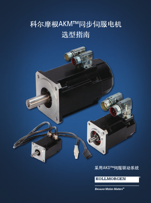
K O L L M O R G E N | A K o l l m o r g e n C O M PA N Y欢迎来到科尔摩根官方微信科尔摩根3目录u AKM ™ 同步伺服电机4u AKD ™ 伺服驱动器8u AKM ™ 各种选件12u AKM ™ 防水型和食品级防水型电机13u AKM ™ 系统综述14u AKM ™ 图纸和性能数据AKM1x 16AKM2x 20AKM3x24AKM4x 28AKM5x 34AKM6x 40AKM7x 44AKM8x48u L 10 轴承疲劳寿命和轴负载53u 反馈选件56u 抱闸选件60u 伺服电机连接器选件61u 型号命名67u MOTIONEERING ® Online71科尔摩根A K M 同步伺服电机选型指南克服设计、采购和时间障碍科尔摩根明白:帮助原始设备制造商的工程师克服障碍,可以显著提高其工作成效。
因而,我们主要通过如下三种方式来提供帮助:集成标准和定制产品在很多情况下,理想方案都不是一成不变的。
我们拥有专业应用知识,可以根据全面的产品组合来修改标准产品或开发全定制解决方案,从而为设计奠定良好的基础。
提供运动控制解决方案而不仅仅是部件在各公司减少供应商数量和工程人力的过程中,他们需要一家能够提供多种集成解决方案的全系统供应商。
科尔摩根就采用了全面响应模式,为客户提供全套解决方案,这些方案将编程软件、工程服务以及同类优秀的运动控制部件结合起来。
覆盖全球我们在美洲、欧洲、中东和亚洲拥有众多直销、工程支持单位、生产工厂以及分销商,临近全球各地的原始设备制造商。
这种便利优势可以加速我们的供货过程,根据客户需要随时随地供货。
财务和运营稳定性科尔摩根隶属于Fortive 公司。
Fortive 业务系统是推动Fortive 各部门发展的一个关键力量。
该系统采用“不断改善”(Kaizen )原理。
由高素质人才构成的多学科团队使用世界级的工具对过程进行评估,并制定相关计划以达到卓越的性能。
同步带
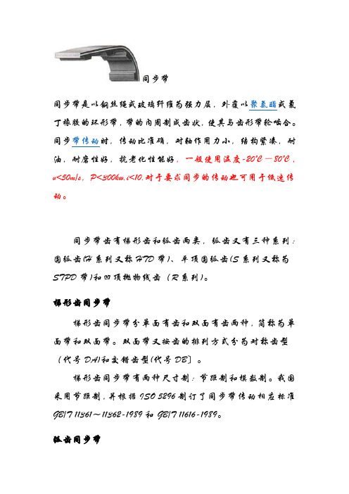
同步带同步带是以钢丝绳或玻璃纤维为强力层,外覆以聚氨酯或氯丁橡胶的环形带,带的内周制成齿状,使其与齿形带轮啮合。
同步带传动时,传动比准确,对轴作用力小,结构紧凑,耐油,耐磨性好,抗老化性能好,一般使用温度-20℃―80℃,v<50m/s,P<300kw,i<10,对于要求同步的传动也可用于低速传动。
同步带齿有梯形齿和弧齿两类,弧齿又有三种系列:圆弧齿(H系列又称HTD带)、平顶圆弧齿(S系列又称为STPD带)和凹顶抛物线齿(R系列)。
梯形齿同步带梯形齿同步带分单面有齿和双面有齿两种,简称为单面带和双面带。
双面带又按齿的排列方式分为对称齿型(代号DA)和交错齿型(代号DB〕。
梯形齿同步带有两种尺寸制:节距制和模数制。
我国采用节距制,并根据ISO 5296制订了同步带传动相应标准GB/T 11361~11362-1989和GB/T 11616-1989。
弧齿同步带弧齿同步带除了齿形为曲线形外,其结构与梯形齿同步带基本相同,带的节距相当,其齿高、齿根厚和齿根圆角半径等均比梯形齿大。
带齿受载后,应力分布状态较好,平缓了齿根的应力集中,提高了齿的承载能力。
故弧齿同步带比梯形齿同步带传递功率大,且能防止啮合过程中齿的干涉。
弧齿同步带耐磨性能好,工作时噪声小,不需润滑,可用于有粉尘的恶劣环境。
已在食品、汽车、纺织、制药、印刷、造纸等行业得到广泛应用。
方形齿同步带型号节距(mm) 齿高(mm) 带厚(mm) 角度β°MXL 2.032 0.51 1.14 40XL 5.080 1.27 2.30 50L 9.525 1.91 3.60 40H 12.70 2.29 4.30 40XH 22.225 6.35 11.20 40XXH 31.750 9.53 15.70 40T2.5 2.5 0.7 1.30 40T5 5 1.20 2.20 40T10 10 2.50 4.50 40T20 20 5.00 8.00 40AT5 5 1.20 2.70 50AT10 10 2.50 5.00 50AT20 20 5.00 8.00 50圆弧齿同步带(高转矩)齿型代号型号节距(mm) 齿高(mm) 带厚(mm) HTD 2M 2 0.75 1.363M 3 1.17 2.45M 5 2.06 3.88M 8 3.36 6.0014M 14 6.02 10.0020M 20 8.4 13.20半圆弧齿同步带(高转矩)齿型代号型号节距(mm) 齿高(mm) 带厚(mm) STPD/STSS2M 2 0.76 1.36S3M 3 1.14 1.9S4.5M 4.5 1.71 2.81S5M 5 1.91 3.4S8M 8 3.05 5.3S14M 14 5.3 10.2RPP/HPPD2M 2 0.76 1.363M 3 1.15 1.95M 5 1.95 3.58M 8 3.2 5.514M 14 6.00 10万方数据库……《浅谈同步带性能及其在玻璃机械上的设计应用》型号…………周节制同步带轮MXL、XL、L、H、XH、XXH特殊节距制同步带轮T2.5、T5、T1、T2、AT3、AT5A、T10、AT15、AT20圆弧齿同带轮S2M、S3M、S4.5M、S5M、S8M、S14M、S20M、2M、3M、5M、8M14M、20M、2GT、3GT、5GT、8GT、14GT、P5M、P8M、P14M、P20M、8YU/view/961b460b76c66137ee0619e9.html参数/kcms/detail/detail.aspx?dbname=CJFD2009&filename=B LZZ200908006知网同步带的参数及性能买家的参数/ArticleShow.asp?ArticleID=106同步带的种类/ArticleShow.asp?ArticleID=105一些参数/ArticleShow.asp?ArticleID=104/ArticleShow.asp?ArticleID=103/ArticleShow.asp?ArticleID=102/ArticleShow.asp?ArticleID=99/view/50f859858762caaedd33d471.html/esite/szcosate/index.html同步带的厂家的信息/一些同步带的种类的图片各种同步带的参数//橡胶方齿同步带:MXL,XL,L,,H,XH,XXH,双面橡胶方齿同步带:DXL,DL,DH圆弧齿同步带:3M,5M,8M,14M,双面圆弧齿同步带:D5M,D8M,聚氨酯同步带:T5,T10,T2.5,AT5,TAT10 (型号)聚氨酯同步带:DT5,DT10橡胶公制同步带:T10,DT10半圆弧齿同步带:S3M,S4.5M,S5M,S8M,S14M,三星普通三角带:K,M,A,B,C,D三星高速防油窄三角带:SPZ,SPA,SPB,SPC三星多沟带:PJ,PL ,PH,PK,PM三星广角带:3M,5M,7M,14M。
因代克斯亮相CIMT2013——聚焦凸轮控制多轴车床的升级换代

对 加工质 量及加 工工艺等 要求 断提
高 ,其 局 限 性 也 日益 突 显 ,例 如 组 建
费用 昂贵、柔性 差且 能耗人 、调试复
杂 要 由 专 业 人 员 操 作 、 需 要 大 量 专 用 刀 具 和 附 具 来 完 成 零 件 的 加 工 、 零 件 的 生产 准 备 工 作 量 大 且 周 期 长 等 。 “ 国 家 十 二 五 规 划 中 明确 提 出 ,
动。典型的 “ 3 + 2 ”模式适合从简单 的
钻孔 到复杂的5 面 体 镗 铣 加 工 。一 次 装 夹 完 成 除 定 位 面 外 的 多面 加 工 , 简 化
于小型车 间的加工任 务 。其 简单巧妙
的 设 计 以及 优 化 的配 置 和 选 项 组 合 , 使M I K R O N H E M 5 0 0 U 成 为 能 胜 任 各 种 工 作环 境 的最 佳 通 用 设 备 。
司的代 表在 现场 谈了大约9 个月 的使用
体 验 : “由于 3 + 2 的机 型 设 计 ,M I K R O N H E M 5 0 0 U 帮 我 们 改 进 了工 艺 , 通 过 改 变 刀 具 的 切 削 路 径 , 同 样 的 零 件 的 加 工 时 间从 1 4 0 m i n 减{  ̄ J 3 5 m i n , 大 大 提 高 了 加 工 效 率 。 同 时 ,公 司 的 刀
5 o o u  ̄ N 工 中心 采 用 强 壮 的 立 柱 型框 架 结构 , 所 有 的部 件 均 由吸 振 性 极好 的 铸 铁 制成 。所 有 的 3 根 线 性 轴 都 位 于 坚 固 的底座 上 端 ,带动 刀 具运 动 , 、 C 旋 转 摆 动 轴 的 移 动 来 带 动 工 件 的 运
Q172运动CPU

Q系列PLC CPU
運動CPU
軟元件存儲器 公共存儲器
順序控制 處理器
軟元件存儲器 公共存儲器
運動控制 處理器
傳感器﹑線圈等(DI/O)
Q系列PLC高速系統總線 PLC智能功能模塊(A/D﹑D/A等)
SSCENT
伺服 放大器
伺服 放大器
伺服
伺服
電機
電機
運動控制專用I/F (DOG信號﹑脈衝信號)
總共﹕ 最多256點/CPU
最多1個/CPU 最多7級 1.25 98(H)×27.4(W)×114.3(D) 0.23
* 注1﹕手動脈衝發生器和同步編碼器加起來共可以使用到12個。
運動CPU單元
Q172CPUN (最大控制8軸)
項目
規格
控制軸數
運行周期 (缺省)
SV13 SV22 SV43
伺服放大器
擴展電纜 QC□B
外圍機器的構成
圖形操作終端 (GOT)
4
擴展基板(注6) (最大7級) Q6□B
(注7) 外接 電池
SSCNET(注7) SSCNET(注7)
運動CPU/ PLC CPU 控制模塊
■ 主機OS軟件包
主機OS軟件(FD) SW6RN-SV□□Q□
傳送裝配用
專用語言
提供等速度控制﹑速度控制﹑1~4軸線性插補﹑2軸圓 弧插補等。 是傳送和裝配機的理想選擇。
伺服電機/ 變頻器用電機(注9)
設備配置
運動CPU輸入/輸出 (最大256點)
外部中斷輸入(16點)
手動脈衝發生器(3個/模塊) MR-HDP01
串行ABS同步編碼器 (2個/模塊) MR-HENC