Zero-Order Hold
光的衍射与光谱学
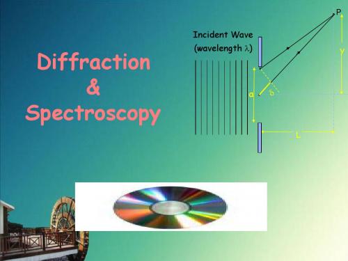
PIncident Wave(wavelength l )yLaDiffraction&SpectroscopyOverview•Multiple-slit Interference formula*•Diffraction Gratings–Optical Spectroscopy–Spectral Resolution•Single-Slit Diffraction*•Interference + Diffraction•X-ray Crystallography*Derivations in AppendixLast Lecture: General properties of N-Slit Interference•The positions of the principal maxima of the intensity patterns alwaysoccur at f = 0, ±2p , ±4p, ...[f is the phase between adjacent slits](i.e., dsin q = ±m l , m = 0, 1, 2,…).•The principal maxima become taller and narrower as N increases.•The intensity of a principal maximum is equal to N 2times the maximum intensity from one slit. The width of a principal maximum goes as 1/N.•The # of zeroes between adjacent principal maxima is equal to N-1. The # of secondary maxima between adjacent principal maxima is N-2.I 016I 1N=40-2p I 025I 1N=502p-2p I9I 1N=31020h5()x 1010x -l/d 0 l/d f q 100100590g()x 1010x fq-l/d 0 l/d 010160h()x 1010x-l/d 0 l/d fqHow do we calculate these interference patterns …illuminates a screen. Now we double the number of slits, keeping the spacing constant.What happens to the net power I on the screen?a. stays same (I)b. doubles (2I)c. increases x4 (4I)illuminates a screen. Now we double the number of slits, keeping the spacing constant. What happens to the net power on the screen?a. stays the same b. doubles c. increases by 4If we double the number of slits, we expect the net power on the screen to double. How does it do this…●The location and number of the principle maxima (whichhave most of the power) does not change.●The principle maxima become 4x brighter.●But they also become only half as wide. (A/2)●Therefore, the net power (integrating over all the peaks) increases two-fold, as we would expect. (P goes as IA)We will soon see that we often use such an array of slits (also called a “diffraction grating”) to perform very precise metrology, e.g, spectroscopy, crystallography, etc.N-Slit Interference –Summary (see Appendix for derivation)•The Intensity for N equally spaced slits is given by:Ly and d sin d ≈⋅≈==q l q l q l δp f 221)2/sin()2/sin(⎪⎭⎫⎝⎛=f f N I I N **Your calculator can probably plot this up. Give it a try.** Note: You will not be able to use the small angle approximations if d ~ l.yLdqf is the phase difference between adjacent slits.•As usual, to determine the pattern at the screen (detectorplane), we need to relate f to q or y = Ltan q :**0 q min ?l /dqIn an N-slit interference pattern, at what angle q min does the intensity first go to zero?(In terms of l , d and N.)What does phasor sum look like here?0 q min ?l /dqIn an N-slit interference pattern, at what angle q min does the intensity first go to zero?(In terms of l , d and N.)But f = 2p(d sin q)/l ≈2p d q /l =2p /N. Therefore, q min ≈l /Nd.As the illuminated number of slits increases, the peak widths decrease!General feature :Wider slit features narrower patterns in the ―far field‖.(obviously doesn‘t hold just past slits!)21sin(/2)sin(/2)N N I I f f ⎛⎫= ⎪⎝⎭has a zero when N f min /2= p , or f min =2p /N.Note:The simple calculations we have done only hold in the ―far-field‖(a.k.a. ―Fraunhofer‖limit), where L >> d2/l.Intermediate cases (―Fresnel diffraction‖) can be much more complex…nearfarOptical spectroscopy –a major window on the world•Quantum mechanics →definite energy levels, e.g., of electrons in atoms or molecules.•When an atom transitions between energy levels →emits light of a very particular frequency.•Every substance has its own “signature” of what colors it can emit.•By measuring the colors, we can determine the substance, as well as things about its surroundings (e.g., temperature, magnetic fields), whether its moving (via the Doppler effect), etc.Optical spectroscopy is invaluable in materials research, engineering, chemistry, biology, medicine…Interference Gratings--the basis for optical spectroscopy Interference gratings (usually called Diffraction gratings) allow us to resolve sharp spectral signals.2/d sin qN-slit Interference:I N = N2I1/d sin q l1l2Shift of the peak:Spectroscopy DemonstrationWe have set up some discharge tubes with various gases. Notice that the colors of the various discharges are quite different. In fact the light emitted from the highly excited gases is composed of many ―discrete wavelengths.‖You can see this with the plastic ―grating‖we supplied.Your eyeHold grating less than 1 inch from your eye.Light sourceYour view throughthe grating:Put light source at left side of grating.View spectral lines by looking at about 45o. If you don’t see anything, rotate grating 90o.Room lights mustbe turned off!Diffraction Gratings (1)•Diffraction gratings rely on N-slit interference.•They simply consist of a large number of evenly spaced parallel slits.•Recall that the intensity pattern produced by light of passing through N slits with spacing d is given by:2122⎭⎬⎫⎩⎨⎧=)/sin()/N sin(I I N f f where:01020h5()x 1010x f 0-2p 025I 1N=5dsin 2q f p l =Consider very narrow slits (), so is roughly constant.y L dq Slits Demo 500/550 nm•The position of the first principal maximum is given by (can ‘t assume small q !) →Different colors →different angles.Diffraction Gratings (2)•How effective are diffraction gratings at resolving light of different wavelengths (i.e. separating closely-spaced‗spectral lines‘)?–Concrete example:Na lamp has a spectrum with two yellow―12Dl =nm)–Are these two lines distinguishable using a particular grating?I N = N2I1/d sin q2/d sin ql1 l2min min sin d dd Nd l l q q l l q D =→D ≈D →D ≈=wavelength separation we can resolve Dl min ≡l 2-l 1occurs when the maximum of l 2overlaps with the first diffraction minimum of l 1.(Dq min =l /Nd)I N = N 2I 1N 1 m in =l l D Larger N Smaller Dl min(Higher spectral resolution)0 l 1/N d sin qq l 1/d “Rayleigh Criterion”N = number of illuminated lines in grating.Dq minl 2/d•We can squeeze more resolution out of a given grating by working in ―higher order ‖. Remember, the principal maxima occur at sin q = m l /d , where m = 1,2,3…designates the ―order ‖. (Dq min ≈ l /Nd still *)You caneasily show:Nm 1m in =l l D qFirst order Second order Third order m = 1m = 2m = 3* To be precise: Dq = l /(Nd cos q ), (but Dl /l = 1/Nm is correct.)Larger Nm Smaller Dl min(Higher spectral resolution)Example: Diffraction Gratings•Angular splitting of the Sodium doublet:Consider the two closely spaced spectral (yellow ) lines of sodium (Na ), l 1= 589 nm and l 2= 589.6 nm .If light from a sodium lamp fully illuminates a diffraction grating with 4000 slits/cm , what is the angular separation of these two lines in the second-order (m=2)spectrum?Hint: First find the slit spacing d from the number of slits per centimeter.Solution•Angular splitting of the Sodium doublet:Consider the two closely spaced spectral (yellow ) lines of sodium (Na ), l 1= 589 nm and l 2= 589.6 nm , mentioned earlier.If light from a sodium lamp illuminates a diffraction grating with 4000 slits/cm , what is the angular separation of these two lines in the second-order (m=2)spectrum?41cm 2.510 2.54000d cm m μ-==⨯=111sin = 28.112 m d l q -⎛⎫=︒ ⎪⎝⎭Hint: First find the slit spacing d from the number of slits per centimeter.1121sin sin 0.031m m d d l l q --⎛⎫⎛⎫D =-=︒ ⎪ ⎪⎝⎭⎝⎭problem (d = 2.5 m), how big must it be to resolve the Na lines (589 nm, 589.6 nm)?(a)0.13 mm(b)1.3 mm(c) 13 mm2. How many interference orders can be seen with this grating?(a)2(b)3(c) 43. Which reduces the maximum number of interference orders?(a) Increase wavelength(b) Increase slit spacing(c) Increase number of slitsproblem (d = 2.5 μm), how big must it be to resolve the Na lines (589 nm, 589.6 nm)?(a)0.13 mm (b)1.3 mm (c) 13 mm3. Which reduces the maximum number of interference orders?(a) Increase wavelength(b) Increase slit spacing(c) Increase number of slits We need enough lines to narrow the diffraction peak:1Nml l D =589nm 4912(0.6nm)N m l l ≥==D size = N d≥490(2.5 μm)≈1.2 mm 2. How many interference orders can be seen with this grating? The diffraction angle can never be more than 90˚: From sin q = m l /d , it must be that m l ≤ d , or m ≤ d/l = 2.5 μm/0.589μm = 4.2 m = 4Increase l , or decrease d. Changing the number of slits does not affect the number of orders.(a)2(b)3(c) 4•So far in the N-slit problem we have assumed that each slit is a point source.–Point sources radiate equally in all directions.–Real slits have a non-zero extent –-a ―slit width ‖a . The transmission pattern depends on the ratio of a l . –In general, the smaller the slit width, the more the wave will diffract!Laser Light (wavelength l )Diffraction profile I 1Small slit:Laser Light (wavelength l )profileI 1Large slit:Single-slit ―Diffraction ‖Laser DemoSingle-Slit Diffraction •Slit of width a. Where are the minima?–The first minimum is at an angle such that the light fromthe top and the middle of theslit destructively interfere:–The second minimum is at an angle such that the light from the top and a point at a/4Location of nth-minimum:PIncident Wave(wavelength l )yLaq a/2δmin sin 22a l δq ==min sin alq ⇒=min,2sin 42a lδq ==min,22sin l q ⇒=min,sin n n a lq =qa/4δ(n = 1, 2, …)Diffraction: Example ProblemSuppose that when we pass red light (l= 600 nm) through a slit of width a, the width of the spot (the distance between the first zeros on each side of the bright peak) is W = 1 cm on a screen that is L = 2m behind the slit. How wide is the slit?a 1 cm = W2 mSolutionSuppose that when we pass red light (l = 600 nm) through a slit of width a , the width of the spot (the distance between the first zeros on each side of the bright peak) is W = 1 cm on a screen that is L = 2m behind the slit. How wide is the slit?Solution:The angle to the first zero is: q = ±l /a1 cm = WL = 2 maqSolve for a: a =2L l /W = (4m)(6⨯10-7m) /(10-2m)= 2.4⨯10-4m = 0.24 mmW = 2 Ltan q ≅ 2 L q = 2L l /a(use tan q ≅q)Which of the following would broaden the diffraction peak?a. reduce the laser wavelength b. reduce the slit widthc. move the screen further away2 ma1 cm = Wa 1 cm = W2 mWhich of the following would broaden the diffraction peak?a. reduce the laser wavelengthb. reduce the slit widthc. move the screen further away胰腺癌患者复查间期内需警惕哪些表现? /a/yixianaikangfu/2015/0107/235.htmlSingle-slit Diffraction —Summary (see Appendix for derivation)form:Single Slit Diffraction Features:•First zero: b/2= p ⇒q ≈l /a(agrees with phasor analysis)100100.5110dif f()x 12.5612.56x b q-4p -2p 0 2p 4p -l/a 0 l/a 0I I 0At P, the phase difference b between 1st and last source is given by:201)/a sin(I )(I ⎪⎫ ⎛=l q p q Screen(far away)δa = a sin q ≈a q qaLq =lq ≈l q =l δ=p b L y a sin a 2a Therefore,P2012/)2/sin(I I ⎪⎭⎫ ⎝⎛=b b b = angle between 1st and last phasorSummary: Slit Interference + DiffractionCombine:Multi-slit Interference,andSingle-slit Diffraction,to obtainTotal Interference Pattern,Remember:f/2p = δ/l = (d sin q)/l ≈d q /lb/2p = δa /l = (a sin q)/l ≈a q/l2012/)2/sin(⎭⎬⎫⎩⎨⎧=b b I I 21)2/sin()2/sin(⎪⎭⎫ ⎝⎛=f f N I I N 22)2/sin()2/N sin(2/)2/sin(I I ⎭⎬⎫⎩⎨⎧f f ⎭⎬⎫⎩⎨⎧b b = f = angle between adjacent phasors b = angle between 1st and last phasor(for plane-wave sources, I 1= constant)Light of wavelength l is incident on an N -slit system with slit width a and slit spacing d .1. The intensity I as a function of y at a viewing screen located a distance L from the slits is shown to the right. What is N ? (L >> d , y , a)(a)N = 2(b)N = 3(c)N =400590intensity ()x 18.8418.84x0Imax 0+6-6Y (cm)2. Now the slit spacing d is halved , but the slit width a is kept constant . Whichof the graphs best represents the new intensity distribution?(a)59intensity ()x II max (c)59intensity ()x II max (b)59intensity ()x II maxLight of wavelength l is incident on an N -slit system with slit width a and slit spacing d .1. The intensity I as a function of y at a viewingscreen located a distance L from the slits is shown to the right. What is N ? (L >> d , y , a)(a)N = 2(b)N = 3(c)N =400590intensity ()x 18.8418.84x0Imax 0+6-6Y (cm)2. Now the slit spacing d is halved , but the slit width a is kept constant . Which of the graphs best represents the new intensity distribution?(a)59intensity ()x II max (c)59intensity ()x II max (b)59intensity ()x II max N is determined from the number of minima between two principal maxima. Here, there are two minima between principal maxima. Therefore, N = 3 .Lecture 3, ACT 400590intensity ()x 18.8418.84x0II max 0+6-6Y (cm)2. Now the slit spacing d is halved , but the slit width a is kept constant .Which of the graphs best represents the new intensity distribution?(a)590intensity ()x 18.8418.84x 0+6-6Y(cm)0II max (c)00590intensity ()x 9.429.42x 0+6-6Y (cm)II max (b)00590intensity ()x 9.429.42x 0+6-6Y (cm)0II max Decreasing d will increase spacing between maxima.The spacing between maxima is increased , but diffractionprofile shouldn ’t expand, as seen here.This one does it all.Increased spacing between maxima and constant diffraction.Light of wavelength l is incident on an N -slit system with slit width a and slit spacing d .1. The intensity I as a function of y at a viewingscreen located a distance L from the slits is shown tothe right. What is N ? (L >> d , y , a)(a)N = 2(b)N = 3(c)N =4•Diffraction gratings are excellent tools for studying visible light because the slit spacing is on the order of the wavelength of the light (~ few tenths of microns)•Visible light is a very small part of the spectrum of electromagnetic waves. How can we study e-m waves with smaller wavelengths (e.g., x-rays with l~ 10-10m)?–We can‘t use a standard diffraction grating to do this.Why?Calculate q for first order peak for x-rays with l = 10-10 m for a grating with d=1000 nm•Solution? We need a ―diffraction ‖grating with a spacing d that is on the order of the wavelength of e-m waves we ‘d like to measure -i.e., for x-rays: l ~10-10m –Where do we find such a ―grating ‖? Nature to the rescue!!!Crystalline solids (having regularly spaced atoms with d ~ 10-10m) naturally occur.iona 0a 0X-rays Diffraction: A Primer •Illuminate crystal with x-rays.•The X-rays are scattered by the ions.•Enhanced scattering at certain scattering angles revealconstructive interference betweenX-ray Diffraction for Crystallography (FYI)•If we know about the grating, we can use the diffraction pattern to learn about the light source.•If instead we know about the source, we can use the diffraction pattern to learn about the ―grating ‖.•For this to work, we need to have a source wavelength that is less than the grating spacing (otherwise, there are no orders of diffraction).•Crystals consist of regularly spaced atoms →regular array of scattering centers. Typical lattice spacing is 5 angstroms = 5 x 10⁻¹⁰m = 0.5 nm.→use x-rays!Bragg Law forconstructive interference:2d sin q = ld = lattice spacing q = x-ray angle (with respect to plane of crystal)l = x-ray wavelengthX-ray Crystallography, misc.•could distinguish different cubic lattices •discovered the crystal structure of diamond •Lawrence Bragg was the youngest Laureate ever (25) to receive a Nobel Prize (shared with his father in 1915)•now standardly used for all kinds of materials analysis, even biological samples!•The same multi-layer interferencephenomenon is now used to make highly wavelength-specific mirrors for lasers (―distributed Bragg feedback‖ [DBF])The Braggs made so many discoveries that Lawrence described the first few years as ‗like looking for gold and finding nuggets lying around everywhere ‘:•showed that the sodium and chloride ions were not bonded into molecules, but arranged in a latticeAppendix: N-Slit Interference •Intensity for N equally spaced slits is easily found from phasor analysis:Draw normal lines bisecting the phasors. They intersect, defining R as shown:221f sin R A =22f N sin R A N =)/sin()/N sin(A A N 221f f =Solve for R and plug in here:Result:2122⎪⎭⎫ ⎝⎛=)/sin()/N sin(I I Nf f fN fA NR A 1RN slits:1f fRR2f2f2f2f2f NAppendix: Single-slit Diffraction•To analyze diffraction, we treat it as interferenceof light from many sources (i.e. the Huygenswavelets that originate from each point in the slitopening).•Model the single slit as M point sources withspacing between the sources of a/M. We will letM go to infinity on the next slide.•The phase difference b between first and lastsource is given by b/2p = δa/l= a sin q / l ≈a q/l .Destructive interference occurs when thepolygon is closed (b= 2p):Slits Demo 10-slits f aA1 (1 slit)A a(1 source)aM fb≈PScreen(far away)δa= a sin q ≈a qqaL >> a implies rays areparallel.La,smallForsinameanshisTlqqlq≈=1DestructiveInterferenceSingle-slit Diffraction —the math•We have turned the single-slit problem into the M-slit problem that we already solved in this lecture.•However, as we let M →∞, the problem becomes muchsimpler because the polygon becomes the arc of a circle.•The radius of the circle is determined by the relationbetween angle and arc length: b = A o /R.2012/)2/sin(I I ⎪⎭⎫ ⎝⎛=b b Graph this functionIntensity is related to amplitude: I = A 2. So, here ‘s the final answer:Remember:b /2p = δa /l = (a sin q)/l ≈a q/lb = angle between 1st and last phasorA oqlpb a 2=A 1b /2RTrigonometry: A 1/2 = R sin(b /2)With R = A o /b , A 1= (2A o /b) sin(b /2)2201/)/sin(A A b b =。
安川伺服驱动说明书

8.5 速度控制 ( 模拟量电压指令 ) 运行 - - - - - - - - - - - 8-33
8.5.1 用户参数的设定 - - - - - - - - - - - - - - - - - - - - - - 8-33 8.5.2 输入信号的设定 - - - - - - - - - - - - - - - - - - - - - - 8-33 8.5.3 指令偏移量的调整 - - - - - - - - - - - - - - - - - - - - - 8-34 8.5.4 软起动 - - - - - - - - - - - - - - - - - - - - - - - - - - 8-37 8.5.5 速度指令滤波器 - - - - - - - - - - - - - - - - - - - - - - 8-37 8.5.6 零箝位功能的使用 - - - - - - - - - - - - - - - - - - - - - 8-38 8.5.7 编码器信号输出 - - - - - - - - - - - - - - - - - - - - - - 8-39 8.5.8 同速检测输出 - - - - - - - - - - - - - - - - - - - - - - - 8-40
8.2 控制方式的选择 - - - - - - - - - - - - - - - - - - - 8-15
8.3 通用基本功能的设定 - - - - - - - - - - - - - - - - - 8-16
8.3.1 伺服 ON 设定 - - - - - - - - - - - - - - - - - - - - - - - - 8-16 8.3.2 电机旋转方向的切换 - - - - - - - - - - - - - - - - - - - - 8-16 8.3.3 超程设定 - - - - - - - - - - - - - - - - - - - - - - - - - 8-17 8.3.4 保持制动器的设定 - - - - - - - - - - - - - - - - - - - - - 8-19 8.3.5 伺服 OFF 时的停止方法选择 - - - - - - - - - - - - - - - - - 8-22 8.3.6 瞬间停电的处理设定 - - - - - - - - - - - - - - - - - - - - 8-23
Ground Control 3.0 级别系统说明书

Ground Control® 3.0 TROUBLESHOOTING GUIDESystem and Safety InformationFailure to act in accordance with the following may result in death or serious personal injury. The use of the Ground Control® 3.0 leveling system to support the trailer for any reason other than which it is intended is prohibited by Lippert’s limited warranty. The Lippert leveling system is designed as a “leveling” system only and should not be used to provide service for any reason under the trailer such as changing tires or servicing the leveling system. Any attempts to change tires or perform other service while trailer is supported by the Ground Control 3.0 leveling system could result in damage to the 5thwheel and/or cause death or serious injury.Moving parts can pinch, crush or cut. Keep clear and use caution.TABLE OF CONTENTSSystem and Safety Information 2Prior To Operation 3Touch Pad Diagram 3Operation4Basic Jack Operation4Unhitching From A Tow Vehicle 4Auto Level5Auto Level Sequence 5Hitch Recognition 5System Settings 6Homing Jacks6Zero Point Calibration 6Troubleshooting 7Manual Override7Touch Pad Error Codes 8Special Jack Error Codes 9Wiring Diagram - 4 Point 10Wiring Diagram - 6 Point11GROUND CONTROL ® 3.0 4 POINT ASSEMBLY 12GROUND CONTROL ® 3.0 6 POINT ASSEMBLY13GROUND CONTROL ® 3.0 4 POINT AFTERMARKET ASSEMBLY 14GROUND CONTROL ® 3.0 6 POINT AFTERMARKET ASSEMBLY 15GROUND CONTROL ® 3.0 COMPONENTS16-19Prior to OperationThe leveling system should only be operated under the following conditions:1. The trailer is parked on a reasonably level surface.2. Be sure all persons, pets, and property are clear of the trailer while the leveling system is in operation.3. Make sure battery(ies) are fully charged and test at 12+VDC under load.Touch Pad DiagramAF H GB C DJ IKFig. 1ECallout DescriptionA Up Arrow - Scrolls up through the menu on LCD.B Down Arrow - Scrolls down through the menu on LCD.C Enter - Activates modes and procedures indicated on LCD.D Retract - Places leveling system into retract mode. Pressand hold down for 1 second to initiate Auto Retract.E LCD Display - Displays procedures and results.F Auto Level - Places leveling system into auto level mode.G Front Jack Button - Activates front jacks in manual mode.H Left Jack Button - Activates left jacks in manual mode.I Right Jack Button - Activates right jacks in manual mode.J Rear Jack Button - Activates rear jacks in manual mode.K Power Button - Turns leveling system on and off.Basic Jack OperationLanding gear (front jacks) can be operated any time the system is “ON.” By pushing the “FRONT” button (Fig. 1G), both front jacks can be extended. By pushing either the "FRONT" and “LEFT” (Fig. 1H) or "FRONT" and “RIGHT” (Fig. 1I) buttons, the individual front jacks can be extended. If the touch pad is put in the retract mode, indicated by the orange illuminated LED next to the “RETRACT” button (Fig. 1D), the front jacks can be retracted together by pushing the “FRONT” button (Fig. 1G) or individually by pressing “LEFT” (Fig. 1H) or “RIGHT” (Fig. 1I) buttons, while simultaneously pressing the “FRONT” button (Fig. 1G).Middle jacks, if equipped, can not be extended or retracted in standard mode or manual mode. Middle jacks can only be operated in the special jack code error mode. In order to operate the middle jacks press "LEFT" (FIG. 1H) and "RIGHT" (FIG. 1I) buttons simultaneously.The rear jacks can only be extended when the touch pad is in the manual mode. Once system is in manual mode, pressing the “REAR” button (Fig. 1J) will extend both rear jacks at the same time. To extend individual rear jacks, press the “LEFT” (Fig. 1H) or “RIGHT” (Fig. 1I) buttons while simultaneously pressing the “REAR” button (Fig. 1J),depending on which jack needs to be operated. If the touch pad is put in the retract mode, indicated by the orange illuminated LED next to the “RETRACT” button (Fig. 1D), the rear jacks can be retracted together by pushing the “REAR” button (Fig. 1J) or individually by pressing either the “LEFT” (Fig. 1H) or “RIGHT” (Fig. 1I) buttons, while simultaneously pressing the “REAR” button (Fig. 1J).NOTE: If the rear jacks will not operate individually using the method described above, but they operateproperly when Auto Level is performed, the Twist Prevention Protection system has locked out the operation to prevent damage to the frame of the trailer.Unhitching From A Tow VehicleNOTE: Prior to unhitching from the tow vehicle, ensurethe trailer is parked on a level surface and be sure to chock the tires of the trailer.1. Extend the inner legs of both landing gear (front jacks) to within 4-5" of the ground by pulling on the quick-release pins.2. Push “ON/OFF” (Fig. 1K). LCD Screen will light up and display “READY JACKS: UP” (Fig. 2A).3. Push the “UP” arrow (Fig. 1A) to scroll to “Drop Front Jacks” option on LCD screen.4. Red indicator lights (Fig. 2B) may come on, indicating the current disposition of the trailer. In this case, the front and right sides of the trailer are low.5. Push “ENTER” (Fig. 1C). Both front jacks will go to ground and stop.6. Push the “FRONT” button (Fig. 1G) extending the front jacks to a sufficient height, which raises the front of the trailer off of the tow vehicle’s 5th wheel hitch plate.7.Pull tow vehicle away and park at a safe distance.Fig. 2BAOperationBe sure to park the trailer on solid, level ground. Clear all jack landing locations of debris and obstructions. Locations should also be free of depressions. When parking the trailer on extremely soft surfaces, utilize load distribution pads under each jack. People and pets should be clear of trailer while operating leveling system. Never lift the trailer completely off the ground. Lifting the trailer so thewheels are not touching the ground will create an unstable and unsafe condition.Fig. 3Auto Level1.After unhitching from tow vehicle and parking the vehicle at a safe distance away from the trailer, press the “ON/OFF” button (Fig. 1K) and then press “AUTO LEVEL” (Fig. 1F).NOTE: Once the automatic leveling cycle has been started, it is important that there is no movement in thetrailer until the trailer has completed the leveling process. Failure to remain still during the leveling cycle could have an effect on the performance of the leveling system.NOTE: In order for hitch recognition feature to function, the auto level sequence must be started with thefront of the trailer above level.Auto Level Sequence1. When Auto Level Sequence begins, the front of the trailer will lower slightly to a point below level.2. Rear jacks will be grounded.3.A side-to-side leveling sequence occurs.NOTE: At this point on the 6 Point System, the 2 middle jacks are grounded to stabilize the trailer. These 2jacks do not level the trailer.4. Each jack will perform a final grounding touch.5. LCD will read “AUTO LEVEL SUCCESS” (Fig. 3A).6.LCD will then read “READY Jacks: Down” (Fig. 4A), and the green LED at the center of the 4 jack buttons will be illuminated (Fig. 4B).NOTE: If the AUTO LEVEL sequence does not perform as described, place the system in manual mode andtest that the jacks operate correctly by pushing their coordinating buttons on the touch pad; i.e. "FRONT" button operates only the front jacks, etc.Fig. 4ABAHitch Recognition1. Turn on the touch pad.2. Push the “UP” arrow (Fig. 1A) to scroll to “Auto Reconnect” option on LCD screen.3.Push "ENTER" (Fig. 1C). The rear jacks and middle jacks (if equipped) will retract first, then the front jacks will extend to raise the trailer to the height where the auto level sequence was started.NOTE: If the auto level sequence was started with the front of the trailer in a below-level condition, theHitch Recognition will not function and the LCD will display “Feature Disabled.” In order for the Hitch Recognition feature to function, the auto level sequence must be started with the front of the trailer above level.System SettingsHoming JacksNOTE: When components are added or replaced the system will need to be homed.1. Run the system by pressing "FRONT" (Fig. 1G). A special jack error code should occur. If not, introducethe special jack error code.NOTE: To introduce an error, disconnect 1 of the hall effect sensor wires from the controller. After attempting to operate the disconnected jack, the touchpad screen will display an error. Reconnectthe hall effect sensor wire.NOTE: In order to clear the special jack error code the jacks need to be "homed." In order to "home" jacks, each jack must be able to retract a minimum of 6".2. Extend all jacks to reach the 6" of minimum retract needed.A. Press "FRONT" (Fig. 1G) to extend the front jacks (if required).B. Press "REAR" (Fig. 1J) to extend the rear jacks (if required).C. Press "LEFT" and "RIGHT" (Fig. 1H and Fig. 1I) simultaneously to extend the middle jacks (ifequipped and required).3. Press and hold the retract button until all of the jacks begin to retract. The jacks will retract until theyreach the hard current limit.4. The jacks are now “homed” and the special jack error code will be cleared.NOTE: If the jacks do not retract, an error should display on the touch pad screen. This is typically caused by wiring interruption.Zero Point CalibrationThe “Zero Point” is the programmed point that the trailer will return to each time the Auto Level feature is used.NOTE: Prior to starting this procedure, double check all connections on the controller, jacks, and touch pad.1. In manual mode, run the jacks to level the trailer. This is best achieved by placing a level in the centerof the trailer and leveling it both front to back and then side to side. (See “Basic Jack Operation” forinstructions on how to manually operate the system).2. Once the trailer is level, turn off the touch pad.3. With the touch pad off, press and release the “FRONT” button (Fig. 1G) 5 times and then press andrelease the “REAR” button (Fig. 1J) 5 times.4. The touch pad will flash and beep and the display will read “ZERO POINT CALIBRATION ENTER to set,Power to Exit” (Fig. 5).5. To set the current position as the zero point, press the “ENTER” button (Fig. 1C).6. LCD display will read “Zero point stability check” (Fig. 6).7. LCD display will read “Zero point set successfully” once process is complete (Fig. 7).8. The system will set this point as its level state and the touch pad will turn off.Fig. 5 Fig. 6 Fig. 7TroubleshootingEnsure the trailer is supported at both the front and rear with jack stands before performing any troubleshooting or service to the trailer. Failure to do so may result in death or personal injury.Manual OverrideNOTE: For ease of manual override it is recommended to unplug the power harness to the motor prior toperforming the manual override procedure. NOTE: Use of a 12-18 volt cordless screw gun or pneumatic screw gun is acceptable to manually overridethe jacks. Do not use an impact screw gun to perform any of the override procedures, as this may damage the motor. If manual override is necessary there are two options.Top of Jack Motor Override:Tools needed: 3/8” drive ratchet and extension (no socket)1. Find the port on the top of the jack motor (Fig. 8A).2. Remove the rubber plug (Fig. 9A).3. Insert the 3/8” drive into the port (Fig. 10).4.Turn override until the jack extends or retracts to desired position.AFig. 9Fig. 11 AFig. 10Fig. 12Fig. 8ABBottom of Jack Motor Override:Tools needed: 3/8” drive ratchet and extension, 5/16” socket1.Find the port on the bottom of the jack motor (Fig. 8B).2. Remove the rubber plug (Fig. 11A).3. Insert the 5/16” socket into the port (Fig. 12).4.Turn override until the jack extends or retracts to desired position.NOTE: To clear an error code from the touch pad, repair or otherwise correct the issue, then press “ENTER.”If the error is still present, the message will be displayed again.LCD Message What's Happening?What Should Be Done?****ERROR**** Excess Angle Controller not properly secured.Check and secure controller placement. Excessive angle reached during autooperation.Relocate the trailer.****ERROR**** Excessive Angle Controller not properly secured.Check and secure controller placement. Excessive angle reached during autooperation.Relocate the trailer.****ERROR**** Feature Disabled Front of trailer below level whenstarting Auto Level process (only whentrying to initiate Hitch Recognition).Using manual mode on the touch pad, retract rear jacks(which includes the middle, if equipped) and set landinggear (front jacks) to hitch height.Touch pad power not cycled betweenconsecutive leveling operations.Turn touch pad off and then back on to reset the system. Zero point not set.Set zero point.****ERROR****Low Voltage Battery voltage dropped below 10.8V.Check wiring - repair or replace.Test battery voltage under load - charge or replace.****ERROR**** Out Of Stroke Jack has reached maximum strokelength and is unable to lift.Check disposition of jacks. Relocate the trailer. Unexpected high amp current stall.Check jacks in manual mode or perform manual overrideprocedure. Repair or replace as needed.Check for bent or damaged jacks. Repair or replace asneeded.****ERROR**** External Sensor Bad connection or wiring from thecontroller to the rear sensor.Replace or repair connection to rear remote sensor.****ERROR**** Jack Time Out Time limit exceeded for the requestedauto operation.Check disposition of jacks.****ERROR**** Auto Level Fail Unable to auto level due to unevenground.Check disposition of jacks. Relocate the trailer. Unable to auto level due to zero pointbeing set incorrectly.Reset zero point.****ERROR**** Comm Error Communication between controllerand touch pad has been lost.Check harness for proper connections or damage.Replace if necessary.****ERROR**** Bad Calibration Sensor calibration values are out ofrange.Replace controller.****ERROR****Internal Sensor Internal sensor problem.Replace controller.**PANIC STOP** Function Aborted The user pressed a button on the touchpad during an automatic operation.Restart automatic operation and then refrain frompressing any buttons on the touch pad.****ERROR**** Hall Effect Short Short circuit detected in one of the halleffect circuits.Test for short and repair or replace.To clear 1of the error codes listed below:1. Correct or otherwise repair the issue (see the table below).NOTE: In order to clear the special jack error code the jacks need to be "homed." In order to "home" jacks, each jack must be able to retract a minimum of 6".2. Extend all jacks to reach the 6" of minimum retract needed.A. Press "FRONT" (Fig. 1G) to extend the front jacks (if required).B. Press "REAR" (Fig. 1J) to extend the rear jacks (if required).C. Press "LEFT" and "RIGHT" (Fig. 1H and Fig. 1I) simultaneously to extend the middle jacks (ifequipped and required).3. Press and hold the retract button until all of the jacks begin to retract. The jacks will retract until theyreach the hard current limit.4. The jacks are now “homed” and the special jack error code will be cleared.NOTE: If the jacks do not retract, an error should display on the touch pad screen. This is typically caused by wiring interruption.LCD Message What's Happening?What Should Be Done?***ERROR*** LF Jack RF Jack LM Jack RM Jack LR Jack RR Jack Error at a specific jack (left front, right front,left middle, right middle, left rear, right rear).Hall signal issue (open, short, malfunction orloss of communication); open or short circuitbetween controller and motor.Check harness connections atcontroller and at jack.Check harness for damage.Check fuses at controller.Repair or replace as necessary.Wiring Diagram - 4 PointHall Effect Landing GearLCD Touch Pad LCD Touch Pad HarnessRecommended 50 Amp Breaker (OEM Supplied)Hall Effect Landing GearHall Effect Harness Hall Effect Harness Hall Effect JackHall Effect JackBattery4 Point ControllerRear SensorRear Sensor HarnessWiring Diagram - 6 PointBatteryRear SensorRear Sensor HarnessLCD Touch PadTouch Pad Harness6 Point ControllerHall Effect JackHall Effect JackHall Effect Jack Hall Effect JackHall Effect Landing GearHall Effect Landing GearRecommended 50 Amp Breaker (OEM Supplied)Power and GroundHarnessLanding Gear x2Bolt On Pull PinHall Effect Jacks;Right RearLanding GearHarnesses x2Rear JackHarnesses x2Jack MountingBracket x2Snapper Pin x2Jack MountingBolt & Nut x12Carriage Bolt& Lock Nut x4Rear SensorScrew x4Rear SensorMounting Plate4 Point ControllerRear Sensor & HarnessControl SystemHall Effect Jacks;Left RearPower and Ground HarnessLanding Gear x2Bolt On Pull Pin Hall Effect Jacks; Right Rear & Middle x2Landing Gear Harnesses x2Rear Jack Harnesses x4Jack Mounting Bracket x4Snapper Pin x4Jack Mounting Bolt & Nut x24Carriage Bolt & Lock Nut x4Rear Sensor Screw x4Rear Sensor & HarnessControl SystemRear Sensor Mounting Plate6 Point Controller Hall Effect Jacks; Left Rear & Middle x2Power and GroundHarnessHall EffectJacks; Left RearLandingGear x2Bolt OnPull Pin Landing Gear Harnesses x2Rear JackHarnesses x2Snapper Pin x2Jack MountingBolt & Nut x12Carriage Bolt & Lock Nut x4Rear SensorScrew x4Rear Sensor & HarnessControl SystemJack MountingBracket x2Rear SensorMounting Plate4 Point ControllerHall Effect Jacks; Right RearPower and Ground HarnessLanding Gear x2Bolt On Pull Pin Hall Effect Jacks; Right Rear & Middle x2Landing Gear Harnesses x2Rear Jack Harnesses x4Snapper Pin x4Jack Mounting Bolt & Nut x24Carriage Bolt & Lock Nut x4Rear Sensor Screw x4Rear Sensor & HarnessControl SystemJack Mounting Bracket x2Rear Sensor Mounting Plate6 Point Controller Hall Effect Jacks; Left Rear & Middle x2B CADGHEFCallout Part #DescriptionA305340Hall Effect Landing Gear; Front Stroke 19.8125"B305339Left Hall Effect Jack; Rear and Middle 12.5" StrokeC344792Right Hall Effect Jack; Rear and Middle 12.5" StrokeD342610Hall Effect Jack; Rear Short 10.5" StrokeE343758Hall Effect Jack MotorF119113Bolt On Pull PinG134989Weld On Jack Mounting Bracket (OEM Only)H349975Bolt On Jack Mounting Bracket (Aftermarket Only)MPONLKIJCallout Part #DescriptionI 178210Jack Mounting Nut; 1/2" - 20J 118076Jack Mounting Bolt; 1/2" - 20 x 1 1/2" Flange K 119073Top Lock Nut L 125878Carriage BoltM 225598Snapper Pin; 3/8 x 3"N 241940Rear Sensor Mounting ScrewO 191021Hex Head Bolt (Aftermarket Only)P231775Rear Sensor Mounting PlateQUVWXRSTCallout Part #Description Q 232201Rear SensorR 232937LCD Touch Pad Harness S 243688Rear Sensor Harness T 267401Linc Remote Charger U 234802LCD Touch Pad V 329164Linc RemoteW 304136 4 Point Hall Effect Canbus Wireless Ground Control Controller X346005 6 Point Hall Effect Canbus Wireless Ground Control ControllerZY Callout Part #DescriptionY 305115Hall Effect Right Rear Sensor Harness 306298Hall Effect Left Rear Sensor Harness 307489Hall Effect Right Front Sensor Harness 307490Hall Effect Left Front Sensor Harness 347012Hall Effects Right Middle Sensor Harness 347013Hall Effects Left Middle Sensor HarnessZ306176Power and Ground Supply HarnessThe contents of this manual are proprietary and copyright protected by Lippert Components, Inc. (“LCI”). LCI prohibits the copying or dissemination of portions of this manual unless prior written consent from an authorized LCI representative has been provided. Any unauthorized use shall void any applicable warranty. The information contained in this manual is subject to change without notice and at the sole discretion of LCI.Revised editions are available for free download from .Please recycle all obsolete materials.For all concerns or questions, please contactLippert Components, Inc.Ph: (574) 537-8900 | Web: | Email: ************************。
同惠th2830 系列仪器使用说明书
V 2.0版本历史:*******————————————————————2020/8/12本说明书所描述的可能并非仪器所有内容,同惠公司有权对本产品的性能、功能、内部结构、外观、附件、包装物等进行改进和提高而不作另行说明!由此引起的说明书与仪器不一致的困惑,可通过封面的地址与我公司进行联系。
第1章开箱安装14 1.1开箱检查14 1.2电源连接14 1.3保险丝14 1.4环境14 1.5使用测试夹具15 1.6预热15 1.7仪器的其它特性15第2章概述16 2.1前面板说明16 2.2面板说明18 2.3显示区域定义19 2.4主菜单按键和相应显示的页面202.4.1显示主菜单按键[DISP] 202.4.2参数设置主菜单按键[SETUP] 212.4.3系统设置主菜单按键[SETUP] 21 2.5基本操作21 2.6开机22第3章[DISP]菜单键说明233.1<元件测量显示>页面233.1.1测试功能24 3.1.2测试量程26 3.1.3测试频率27 3.1.4测试电平28 3.1.5直流偏置29 3.1.6测试速度29 3.1.7其它工具30 3.2<档号显示>页面30 3.2.1比较器功能31 3.3<档计数显示>页面32 3.3.1参数33 3.3.2标称33 3.3.3档33 3.3.4上下限33 3.3.5计数33 3.3.6附属(AUX) 33 3.3.7超差(OUT) 33 3.4<列表扫描>页面34 3.4.1扫描方式353.4.2频率(Hz) 35 3.4.3 R[:] X[: ] 35 3.4.4 CMP(比较)35 3.5<测量设置>页面36 3.5.1触发方式37 3.5.2自动电平控制功能38 3.5.3平均次数38 3.5.4电平电流监视功能39 3.5.5触发延时39 3.5.6步进延时39 3.5.7输出电阻40 3.5.8直流电阻极性40 3.5.9直流电阻量程40 3.5.10直流电平41 3.5.11偏差测试功能41 3.6<用户校正>页面42 3.6.1开路校正43 3.6.2短路校正45 3.6.3负载校正463.6.4负载校正测试功能47 3.6.5点频校正48 3.6.6电缆长度选择48 3.7<极限列表设置>页面48 3.7.1对调参数49 3.7.2比较功能极限模式49 3.7.3容差方式标称值设置51 3.7.4比较器功能ON/OFF 51 3.7.5附属档ON/OFF 51 3.7.6上下极限52 3.8<列表扫描设置>页面53 3.8.1方式53 3.8.2测试参数可选项53 3.8.3扫描参数设置54 3.9<工具>页面54 3.9.1校正数据55 3.9.2空夹具判别55 3.9.3锁定标称量程55 3.9.4自动返回数据553.9.5 HDL 有效时间55第4章[SYSTEM]菜单键说明和文件管理564.1<系统设置>页面564.1.1仪器功能564.1.2合格讯响564.1.3不良讯响574.1.4显示语言574.1.5口令574.1.6总线方式584.1.7 GPIB地址(预留功能)584.1.8只讲(Talk Only)584.1.9偏置源594.1.10波特率594.1.11菜单保持594.1.12时间60 4.2<文件管理>页面604.2.1单组元件设定文件(*.STA)604.2.2 TH2830系列仪器的优盘管理性能614.2.3文件管理操作步骤:62第5章执行LCR测量操作及一些示例65 5.1“清零”校正操作655.1.1全频清零:655.1.2点频清零(对于使用单个频率测试的情况比较好):65 5.2被测元件的正确连接66 5.3消除杂散阻抗的影响67 5.4用TH2830测试电感快速操作实例68 5.5用TH2830作多频列表扫描测试电容快速操作实例69 5.6比较器设置实例715.6.1电容器分选715.6.2负载校准操作实例72第6章性能与测试74 6.1测量功能746.1.1测量参数及符号746.1.2等效方式746.1.3量程746.1.4触发746.1.5触发延时746.1.6测试端连接方式756.1.7测量速度(频率>=10kHz时)756.1.8平均75 6.1.9显示位数75测试信号75 6.1.10测试信号频率75 6.1.11信号模式75 6.1.12测试信号电平75 6.1.13输出阻抗76 6.1.14测试信号电平监视器76 6.1.15测量显示最大范围76 6.1.16直流偏置电压源76测量准确度76 6.1.17│Z│、│Y│、L、C、R、X、G、B的准确度77 6.1.18 D 准确度77 6.1.19 Q 准确度77 6.1.20θ 准确度78 6.1.21 G 准确度78 6.1.22 Rp 准确度78 6.1.23 Rs 准确度78 6.1.24准确度因子79 6.1.25直流电阻DCR 准确度816.1.26漏电感Lk 准确度82 6.2安全要求826.2.1绝缘电阻826.2.2绝缘强度826.2.3泄漏电流82 6.3电磁兼容性要求82 6.4性能测试826.4.1工作条件826.4.2试验仪器和设备见下表。
ALD500v2单片双斜率积分式ADC
Operating Temperature Range *0°C to +70°C 0°C to +70°C 0°C to +70°C16-Pin 16-Pin16-Pin Wide Body Plastic Pin Small Outline Small Outline PackagePackage (SOIC)Package (SOIC)ALD500PC (16 bit)ALD500SC (16 bit)ALD500SWC (16 bit)ALD500APC (17 bit)ALD500ASC (17 bit)ALD500ASWC (17 bit)ALD500AUPC (18 bit)ALD500AUSC (18 bit)ALD500AUSWC (18 bit)* Contact factory for industrial temperature rangeBENEFITS •Wide dynamic signal range •Very high noise immunity •Low cost, simple functionality•Automatic compensation and cancellation of error sources•Easy to use to acquire true 18 bit,17 bit, or 16 bit conversion and noise performance •Inherently linear and stable with temperature and component variations FEATURES•Resolution up to 18 bits plus sign bit and over-range bit•Accuracy independent of input source impedances•High input impedance of 1012 Ω•Inherently filters and integrates any external noise spikes •Differential analog input•Wide bipolar analog input voltage range ±3.5V•Automatic zero offset compensation •Low linearity error - as low as 0.002%•Fast zero-crossing comparator - 1µs •Low power dissipation - 6mW typical •Automatic internal polarity detection •Low input current - 2pA typical•Microprocessor controlled conversion •Optional digital control from a microcon-troller, an ASIC, or a dedicated digital circuit •Flexible conversion speed versus resolution trade-offALD500AU/ALD500A/ALD500A DVANCED L INEARD EVICES, I NC.ORDERING INFORMATIONPRECISION INTEGRATING ANALOG PROCESSORAPPLICATIONS • 4 1/2 digits to 5 1/2 digits plus sign measurements •Precision analog signal processor •Precision sensor interface•High accuracy DC measurement functions •Portable battery operated instruments •Computer peripheral •PCMCIAGENERAL DESCRIPTIONThe ALD500AU/ALD500A/ALD500 are integrating dual slope analog processors, designed to operate on ±5V power supplies for building precision analog-to-digital converters. The ALD500AU/ALD500A/ALD500 feature specifications suitable for 18 bit/17 bit/16 bit resolution conversion, respectively. Together with three capacitors, one resistor,a precision voltage reference, and a digital controller, a precision Analog to Digital converter with auto zero can be implemented. The digital controller can be implemented by an external microcontroller,under either hardware (fixed logic) or software control. For ultra high resolution applications, up to 23 bit conversion can be implemented with an appropriate digital controller and software.The ALD500 series of analog processors accept differential inputs and the external digital controller first counts the number of pulses at a fixed clock rate that a capacitor requires to integrate against an unknown analog input voltage, then counts the number of pulses required to deintegrate the capacitor against a known reference voltage. This unknown analog voltage can then be converted by the microcontroller to a digital word, which is translated into a high resolution number,representing an accurate reading. This reading, when ratioed against the reference voltage, yields an accurate, absolute voltage measurement reading.The ALD500 analog processors consist of on-chip digital control circuitry to accept control inputs, integrating buffer amplifiers, analog switches,and voltage comparators. It functions in four operating modes, or phases, namely auto zero, integrate, deintegrate, and integrator zero phases. At the end of a conversion, the comparator output goes from high to low when the integrator crosses zero during deintegration.ALD500 analog processors also provide direct logic interface to CMOS logic families.Rev. 1.02 © 1999 Advanced Linear Devices, Inc., 415 T asman Drive, Sunnyvale, California 94089-1706, T el: (408) 747-1155, Fax: (408) 747-1286PIN CONFIGURATIONV +123141516413B 512A V +REF6781011 V -C AZ C INT B UF AGND V -REFC +REF 9V -IN V +IN C OUT DGND PC, SC, SWC PACKAGEC -REF ALD5002Advanced Linear Devices ALD500AU/ALD500A/ALD500GENERAL THEORY OF OPERATIONDual-Slope Conversion Principles of OperationThe basic principle of dual-slope integrating analog to digital converter is simple and straightforward. A capacitor, C INT , is charged with the integrator from a starting voltage, V X , for a fixed period of time at a rate determined by the value of an unknown input voltage, which is the subject of measurement.Then the capacitor is discharged at a fixed rate, based on an external reference voltage, back to V X where the discharge time, or deintegration time, is measured precisely. Both the integration time and deintegration time are measured by a digital counter controlled by a crystal oscillator. It can be demonstrated that the unknown input voltage is determined by the ratio of the deintegration time and integration time, and is directly proportional to the magnitude of the external reference voltage.The major advantages of a dual-slope converter are:a.Accuracy is not dependent on absolute values of integration time t INT and deintegration time t DINT , but is dependent on their relative ratios. Long-term clock frequency variations will not affect the accuracy. A standard crystal controlled clock running digital counters is adequate to generate very high accuracies.b.Accuracy is not dependent on the absolute values of R INT and C INT . as long as the component values do not vary through a conversion cycle, which typically lasts less than 1second.c.Offset voltage values of the analog components, such as V X , are cancelled out and do not affect accuracy.d.Accuracy of the system depends mainly on the accuracy and the stability of the voltage reference value.e.Very high resolution, high accuracy measurements can be achieved simply and at very low cost.An inherent benefit of the dual slope converter system is noise immunity. The input noise spikes are integrated (averaged to near zero) during the integration periods. Integrating ADCs are immune to the large conversion errors that plague successive approximation converters and other high resolution converters and perform very well in high-noise environments.The slow conversion speed of the integrating converter provides inherent noise rejection with at least a 20dB/decade attenuation rate. Interference signals with frequencies at integral multiples of the integration period are, theoretically, completely removed.Integrating converters often establish the integration period to reject 50/60Hz line frequency interference signals.The relationship of the integrate and deintegrate (charge and discharge) of the integrating capacitor values are shown below:V INT = V X - (V IN . t INT / R INT . C INT )FIGURE 1. ALD 500 Functional Block Diagram(14)(15)C OUT DGND Control LogicA B (5)(11)(2)(16)(13)(12)DD SS V -V +INALD500AU/ALD500A/ALD500Advanced Linear Devices 3(integrate cycle)(1)V X = V INT - (V REF . t DINT / R INT . C INT )(deintegrate cycle)(2)Combining equations 1 and 2 results in:V IN / V REF = -t DINT / t INT(3)where:V x =An offset voltage used as starting voltage V INT =Voltage change across C INT during t INT andduring t DINT (equal in magnitude)V IN =Average, or an integrated, value of input voltageto be measured during t INT (Constant V IN )t INT =Fixed time period over which unknown voltage isintegratedt DINT =Unknown time period over which a knownreference voltage is integratedV REF =Reference VoltageC INT =Integrating Capacitor value R INT =Integrating Resistor value Actual data conversion is accomplished in two phases: Input Signal Integration Phase and Reference Voltage Deintegration Phase.The integrator output is initialized to 0V prior to the start of Input Signal Integration Phase. During Input Signal IntegrationPhase, internal analog switches connect V IN to the buffer input where it is maintained for a fixed integration time period (t INT ). This fixed integration period is generally determined by a digital counter controlled by a crystal oscillator. The application of V IN causes the integrator output to depart 0V at a rate determined by V IN and a direction determined by the polarity of V IN .The Reference Voltage Deintegration Phase is initiated immediately after t INT , within 1 clock cycle. During Reference Voltage Deintegration Phase, internal analog switches connect a reference voltage having a polarity opposite that of V IN to the integrator input. Simultaneously the same digital counter controlled by the same crystal oscillator used above is used to start counting clock pulses. The Reference Voltage Deintegration Phase is maintained until the comparator output inside the dual slope analog processor changes state, indicating the integrator has returned to 0V. At that point the digital counter is stopped. The Deintegration time period (t DINT ), as measured by the digital counter, is directly proportional to the magnitude of the applied input voltage.After the digital counter value has been read, the digital counter, the integrator, and the auto zero capacitor are all reset to zero through an Integrator Zero Phase and an Auto Zero Phase so that the next conversion can begin again. In practice, this process is usually automated so that analog-to-digital conversion is continuously updated. The digital control is handled by a microprocessor or a dedicated logic controller.The output, in the form of a binary serial word, is read by a microprocessor or a display adapter when desired.Figure 2. Basic Dual-Slope ConverterFigure 2. Basic Dual-Slope ConverterABSOLUTE MAXIMUM RATINGSSupply voltage, V+ 13.2V Differential input voltage range -0.3V to V++0.3VPower dissipation 600 mW Operating temperature range PC, SC, SWC package 0°C to +70°C Storage temperature range-65°C to +150°CLead temperature, 10 seconds +260°C OPERATING ELECTRICAL CHARACTERISTICST A= 25°C V+= +5.0V V- = -5.0V (V SUPPLY = ±5.0 V) unless otherwise specified; C AZ = C REF = 0.47µf500AU500A 500Parameter Symbol Min Typ Max Min Typ Max Min Typ Max Unit Test Conditions Resolution1530306060µV Note 1Zero-Scale Z SE0.00250.0030.005%Error0.0030.0050.008%0°C to 70°CEnd Point E NL0.0050.0050.0100.0050.015%Notes 1, 2Linearity0.0070.0150.0200°C to +70°CBest Case N L0.00250.0030.0050.0030.008%Notes 1, 2Straight LineLinearity0.0040.0080.0150°C to +70°CZero-Scale TC ZS0.30.60.30.70.30.7µV/°C0°C to +70°C TemperatureCoefficient0.150.30.150.350.150.35ppm/°C Note 1Full-Scale S YE0.0050.0080.01%Symmetry Error(Rollover Error)0.0080.0100.012%0°C to 70°CFull-Scale TC FS 1.3 1.3 1.3ppm/°C0°C to +70°C TemperatureCoefficientInput I IN222pA V IN= 0VCurrentCommon-Mode CMVR V-+1.5V+-1.5V-+1.5V+-1.5V-+1.5V+-1.5VVoltage RangeIntegrator V INT V-+0.9V+-0.9V-+0.9V+-0.9V-+0.9V+-0.9VOutput SwingAnalog Input V IN V-+1.5V+-1.5V-+1.5V+-1.5V-+1.5V+-1.5V AGND = 0VSignal RangeVoltage V REF V-+1V+-1V-+1V+-1V-+1V+-1VReferenceRange4Advanced Linear Devices ALD500AU/ALD500A/ALD500ALD500AU/ALD500A/ALD500Advanced Linear Devices 5DC ELECTRICAL CHARACTERISTICST A = 25°C V + = +5.0V V - = -5.0V (V SUPPLY = ±5.0 V) unless otherwise specified; C AZ = C REF = 0.47µf500AU500A 500Parameter Symbol MinTyp Max MinTyp Max MinTyp Max Unit Test Conditions Supply Current I S 0.61.00.61.00.61.0mA V + = 5V , A =1,B=1Power Dissipation P D 101010mW V SUPPLY = ±5V Positive Supply RangeV +S4.55.54.55.54.55.5VNote 4Negative Supply Range V -S -4.5-5.5-4.5-5.5-4.5-5.5V Note 4Comparator Logic 1,V OH 444V I SOURCE = 400µAOutput High Comparator Logic 0,V OL 0.40.40.4V I SINK = 1.1mAOutput Low Logic 1, Input High V IH 3.5 3.5 3.5VVoltageLogic 0, Input Low V IL 111VVoltageLogic Input Current I L 0.010.010.01µA Comparator Delayt D111µsecNote 5NOTES:1. Integrate time ≥ 66 msec., Auto Zero time ≥ 66 msec., V INT = 4V, V IN =2.0V Full ScaleResolution = V INT /integrate time/clock period2.End point linearity at ±1/4, ±1/2, ±3/4 Full Scale after Full Scale adjustment.3.Rollover Error also depends on C INT , C REF , C AZ characteristics.4.Contact factory for other power supply operating voltage ranges, including Vsupply = ±3V or Vsupply = ±2.5V.5.Recommended selection of clock periods of one of the following:t clk = 0.27µsec, 0.54µsec, or 1.09µsecwhich corresponds to clock frequencies of 3.6864 MHz, 1.8432 MHz, 0.9216 MHz respectively.~Figure 3. ALD500 TIMING DIAGRAMC B INPUTA INPUT 1 Conversion CycleSTARTCONVERSION CYCLEC6Advanced Linear Devices ALD500AU/ALD500A/ALD5001C INT Integrator capacitor connection.2V -Negative power supply.3C AZ The Auto-zero capacitor connection.4BUF The Integrator resistor buffer connection.5AGND This pin is analog ground.6C -REF Negative reference capacitor connection.7C +REF Positive reference capacitor connection.8V -REF External voltage reference (-) connection.9V +REF External voltage reference (+) connection.10V -IN Negative analog input.11V +IN Positive analog input.12A Converter phase control MSB Input.13B Converter phase control LSB Input.14C OUTComparator output. C OUT is HIGH during the Integration phase when a positive input voltage is being integrated and is LOW when a negative input voltage is being integrated. A HIGH-to-LOW transition on C OUT signals the processor that the Deintegrate phase is completed. C OUT is undefined during the Auto-Zero phase. It should be monitored to time the Integrator Zero phase.15DGND Digital ground.16V +Positive power supply.PIN DESCRIPTIONPin No.Symbol DescriptionSwitch FunctionsInput Reference InputAuto ZeroReference V IN =AGNDSystem Connect Polarity Sample Offset Conversion Control Phase LogicSW INSW +R or SW -RSW AZSW RSW GSW SAuto Zero A = 0, B = 1Open Open Closed Closed Closed Open Input Signal A = 1, B = 0ClosedOpenOpenOpenOpenOpenIntegration Reference Voltage A = 1, B = 1Open Closed*Open Open Closed OpenDeintegration Integrator A = 0, B = 0Open Open Open Closed Closed ClosedOutput Zero*SW +R would be closed for a positive input signal. SW -R would be closed for a negative input signal.Table 1. Conversion Phase and Control Logic Internal Analog Switch FunctionsALD500AU/ALD500A/ALD500 CONVERSION CYCLE The ALD500AU/ALD500A/ALD500 conversion cycle takes place in four distinct phases, the Auto Zero Phase, the Input Signal Integration Phase, the Reference Voltage DeintegrationPhase, and the Integrator Zero Phase. A typical measurement cycle uses all four phases in an order sequence as mentioned above. The internal analog switch status for each of these phases is summarized in Table 1.The following is a detailed description of each one of the four phases of the conversion cycle.Auto Zero Phase (AZ Phase)The analog-to-digital conversion cycle begins with the Auto Zero Phase, when the digital controller applies low logic level to input A and high logic level to input B of the analog processor. During this phase, the reference voltage is stored on reference capacitor C REF, comparator offset voltage and the sum of the buffer and integrator offset voltages are stored on auto zero capacitor C AZ. During the Auto Zero Phase, the comparator output is characterized by an indeterminate waveform.During the Auto Zero Phase, the external input signal is disconnected from the internal circuitry of the ALD500AU/ ALD500A/ALD500 by opening the two SW IN analog switches and connecting the internal input nodes internally to analog ground. A feedback loop, closed around the integrator and comparator, charges the C AZ capacitor with a voltage to compensate for buffer amplifier, integrator and comparator offset voltages.This is the system initialization phase, when a conversion is ready to be initiated at system turn-on. In practice the converter can be operated in continuous conversion mode, where AZ phase must be long enough for the circuit conditions to settle out any system errors. Typically this phase is set to be equal to t INT.Input Signal Integration Phase (INT Phase)During the Input Signal Integration Phase (INT), the ALD500AU/ ALD500A/ALD500 integrates the differential voltage across the (V+IN) and (V-IN) inputs. The differential voltage must be within the device's common-mode voltage range CMVR. The integrator charges C INT for a fixed period of time, or counts a fixed number of clock pulses, at a rate determined by the magnitude of the input voltage. During this phase, the analog inputs see only the high impedance of the noninverting operational amplifier input of the buffer. The integrator responds only to the voltage difference between the analog input terminals, thus providing true differential analog inputs.The input signal polarity is determined by software control at the end of this phase: C OUT = 1 for positive input polarity;C OUT = 0 for negative input polarity. The value is, in effect, the sign bit for the overall conversion result.The duration of this phase is selected by design to be a fixed time and depends on system parameters and component value selections. The total number of clock pulses or clock counts, during integration phase determine the resolution of the conversion. For high resolution applications, this total number of clock pulses should be maximized. The basic unit of resolution is in µV/count. Before the end of this phase, comparator output is sampled by the microcontroller. This phase is terminated by changing logic inputs AB from 10 to 11.Reference Voltage Deintegration Phase ( D INT Phase)At the end of the Input Signal Integration Phase, Reference Voltage Deintegration Phase begins. The previously charged reference capacitor is connected with the proper polarity to ramp the integrator output back to zero. The ALD500AU/ ALD500A/ALD500 analog processors automatically selects the proper logic state to cause the integrator to ramp back toward zero at a rate proportional to the reference voltage stored on the reference capacitor. The time required to return to zero is measured by the counter in the digital processor using the same crystal oscillator. The phase is terminated by the comparator output after the comparator senses when the integrator output crosses zero. The counter contents are then transferred to the register. The resulting time measurement is proportional to the magnitude of the applied input voltage.The duration of this phase is precisely measured from the transition of AB from 10 to 11 to the falling edge of the comparator output, usually with a crystal controlled digital counter chain. The comparator delay contributes some error in this phase. The typical comparator delay is 1µsec. The comparator delay and overshoot will result in error timing, which translates into error voltages. This error can be zeroed and minimized during Integrator Output Zero Phase and corrected in software, to within ±1 count of the crystal clock (which is equivalent to within ± 1 LSB, when 1 clock pulse = 1 LSB).Integrator Zero Phase ( I NTZ Phase)This phase guarantees the integrator output is at 0V when the Auto Zero phase is entered, and that only system offset voltages are compensated. This phase is used at the end of the reference voltage deintegration and is used for applications with high resolutions. If this phase is not used, the value of the Auto-Zero capacitor (C AZ) must be much greater than the value of the integration capacitor (C INT) to reduce the effects of charge-sharing. The Integrator Zero phase should be programmed to operate until the Output of the Comparator returns "HIGH". A typical Integrator Zero Phase lasts 1msec.The comparator delay and the controller's response latency may result in Overshoot causing charge buildup on the integrator at the end of a conversion. This charge must be removed or performance will degrade. The Integrator Output Zero phase should be activated (AB = 00) until C OUT goes high. At this point, the integrator output is near zero. Auto Zero Phase should be entered (AB = 01) and the ALD500AU/ ALD500A/ALD500 is held in this state until the next conversion cycle.ALD500AU/ALD500A/ALD500Advanced Linear Devices7Differential Inputs (V+IN,V-IN)The ALD500AU/ALD500A/ALD500 operates with differentialvoltages within the input amplifier common-mode voltagerange. The amplifier common-mode range extends from 1.5V below positive supply to 1.5V above negative supply. Withinthis common-mode voltage range, common-mode rejection istypically 95dB.The integrator output also follows the common-mode voltage. When large common-mode voltages with near full-scale differential input voltages are applied, the input signal drives the integrator output to near the supply rails where the integrator output is near saturation. Under such conditions, linearity of the converter may be adversely affected as the integrator swing can be reduced. The integrator output must not be allowed to saturate. Typically, the integrator output can swing to within 0.9V of either supply rails without loss of linearity.Analog GroundAnalog Ground is V-IN during Auto Zero Phase and ReferenceVoltage Deintegration Phase. If V-IN is different from analogground, a common-mode voltage exists at the inputs. This common mode signal is rejected by the high common mode rejection ratio of the converter. In most applications, V-IN is set at a fixed known voltage (i.e., power supply ground). All other ground connections should be connected to digital ground in order to minimize noise at the inputs. Differential Reference (V+REF, V-REF)The reference voltage can be anywhere from 1V of the powersupply voltage rails of the converter. Roll-over error is caused by the reference capacitor losing or gaining charge due to the stray capacitance on its nodes. The difference in reference for (+) or (-) input voltages will cause a roll-over error. This error can be minimized by using a large reference capacitor in comparison to the stray capacitance.Phase Control Inputs (A, B)The A and B logic inputs select the ALD500AU/ALD500A/ ALD500 operating phase. The A and B inputs are normally driven by a microprocessor I/O port or external logic, using CMOS logic levels. For logic control functions of A and B logic inputs, see Table 1.Comparator Output (C OUT)By monitoring the comparator output during the Input Signal Integration Phase, which is a fixed signal integrate time period, the input signal polarity can be determined by the microcontroller controlling the conversion. The comparator output is HIGH for positive signals and LOW for negative signals during the Input Signal Integration Phase. The state of the comparator should be checked by the microcontroller at the end of the Input Signal Integration Phase, just before transition to the Reference Voltage Deintegration Phase. For very low level input signals noise may cause the comparator output state to toggle between positive and negative states. For the ALD500AU/ALD500A/ALD500, this noise has been minimized to typically within one count.At the start of the Reference Voltage Deintegration Phase, comparator output is set to HIGH state. During the Reference Voltage Deintegration Phase, the microcontroller must monitor the comparator output to make a HIGH-to-LOW transition as the integrator output ramp crosses zero relative to analog ground. This transition indicates that the conversion is complete. The microcontroller then stops and records the pulse count. The internal comparator delay is 1µsec, typically. The comparator output is undefined during the Auto Zero Phase.8Advanced Linear Devices ALD500AU/ALD500A/ALD500APPLICATIONS AND DESIGN NOTESDetermination and Selection of System VariablesThe procedure outlined below allows the user to determine the values for the following ALD500AU/ALD500A/ALD500 system design variables:(1) Determine Input Voltage Range(2) Clock Frequency and Resolution Selection(3) Input Integration Phase Timing(4) Integrator Timing Components (R INT, C INT)(5) Auto Zero and Reference Capacitors(6) Voltage ReferenceSystem TimingFigure 3 and Figure 4 show the overall timing for a typical system in which ALD500AU/ALD500A/ALD500 is interfaced to a microcontroller. The microcontroller drives the A, B inputs with I/O lines and monitors the comparator output, C OUT, using an I/O line or dedicated timer-capture control pin. It may be necessary to monitor the state of the comparator output in addition to having it control a timer directly during the Reference Deintegration Phase.There are four critical timing events: sampling the input polarity; capturing the deintegration time; minimizing overshoot and properly executing the Integrator Output Zero Phase. Selecting Input Integration TimeFor maximum 50/60 cycle noise rejection, Input Integration Time must be picked as a multiple of the period of line frequency. For example, t INT times of 33msec, 66msec and 100 msec maximize 60Hz line rejection, and 20msec, 40 msec, 80msec, and 100 msec maximize 50Hz line rejection. Note that t INT of 100 msec maximizes both 60 Hz and 50Hz line rejection.INT and D INT Phase TimingThe duration of the Reference Deintegrate Phase (D INT) is a function of the amount of voltage charge stored on the integrator capacitor during INT phase, and the value of V REF. The D INT phase must be initiated immediately following INT phase and terminated when an integrator output zero-crossing is detected. In general, the maximum number of counts chosen for D INT phase is twice to three times that of INT phase with V REF chosen as a maximum voltage relative to V IN. For example, V REF = V IN(max)/2 would be a good reference voltage.Integrating Resistor (R INT )The desired full-scale input voltage and amplifier output current capability determine the value of R INT. The buffer and integrator amplifiers each have a full-scale current of 20µA.The value of R INT is therefore directly calculated as follows:R INT=V IN MAX / 20 µA where:V IN MAX=Maximum input voltage desired(full count voltage)R INT=Integrating Resistor valueFor minimum noise and maximum linearity, R INT should be inthe range of between 50kΩ to 150kΩ .Integrating Capacitor (C INT)The integrating capacitor should be selected to maximizeintegrator output voltage swing V INT, for a given integrationtime, without output level saturation. For +/-5V supplies, recommended V INT range is between +/- 3 Volt to +/-4 Volt.Using the 20µA buffer maximum output current, the value ofthe integrating capacitor is calculated as follows:C INT = (t INT) . (20 x 10-6) / V INTwhere:t INT=Input Integration Phase PeriodV INT=Maximum integrator outputvoltage swingIt is critical that the integrating capacitor must have a very lowdielectric absorption, as charge loss or gain during conversiondirectly converts into an error voltage. Polypropylene capacitorsare recommended while Polyester and Polybicarbonatecapacitors may also be used in less critical applications. Reference (C REF) and Auto Zero (C AZ) CapacitorsC REF and C AZ must be low leakage capacitors (e.g.polypropylene types). The slower the conversion rate, the larger the value C REF must be. Recommended capacitor values for C REF and C AZ are equal to C INT. Larger values for C AZ and C REF may also be used to limit roll-over errors.Calculate V REFThe reference deintegration voltage is calculated using: V REF = (V INT) . (C INT) . (R INT) / 2(t INT)Converter NoiseThe converter noise is the total algebraic sum of the integrator noise and the comparator noise. This value is typically 14 µV peak to peak. The higher the value of the reference voltage, the lower the converter noise. Such sources of noise errors can be reduced by increased integration times, which effectively filter out any such noise. If the integration time periods are selected as multiples of 50/60Hz frequencies, then 50/60Hz noise is also rejected, or averaged out. The signal-to-noise ratio is related to the integration time (t INT) and the integration time constant (R INT) (C INT) as follows:S/N (dB) = 20 Log ((V INT / 14 x 10-6) . t INT /(R INT. C INT)) This converter noise can also be reduced by using multiple samples and mathematically averaged. For example, taking 16 samples and averaging the readings result in a mathematical (by software) filtering of noise to less than 4µV.ALD500AU/ALD500A/ALD500Advanced Linear Devices9。
ABB机器人程序指令详解

[\Off]: 默认轴配置数据。
( switch )
直线运动时,机器人移动至 ModPos 点,
轴配置数据默认为当前最接近值。
2020/3/
运动控制指令-ConfL
应用: 对机器人运行姿态进行限制与调整,程序运 行时,使机器人运行姿态得到控制。系统默 认值为 ConfL\On; 。
实例:
ConfL\On; … ConfL\Off;
p10,外轴不动。
p20,外轴联动 track_motion。
p30,外轴联动 orbit_a。
限制: 不能在指令 StorePath …RestoPath 内使用。 不能在预置程序 RESTART 内使用。
2020/3/
计数指令
Add Incr
Clear Decr
2020/3/
计数指令-Add
2020/3/
运动控制指令-SoftAct
SoftAct [\MechUnit,] Axis, Softness [\Ramp];
[\MechUnit]: Axis: Softness: [\Ramp]:
软化外轴名称。 ( mecunit )
软化转轴号码。 ( num )
软化值 %。
( num )
2020/3/
运动控制指令-PathResol
限制: 机器人必须在完全停止后才能更改路径控制
值,否则,机器人将默认一个停止点,并且 显示错误信息 50146。 机器人正在更改路径控制值时,机器人被强 制停止运行,机器人将不能立刻恢复正常运 行 ( Restart )。 以下情况机器人将自动恢复默认值 100%。 机器人冷启动。 系统载入新的程序。 程序重置 ( Start From Beginning )。
xilinx官方论坛解释时序约束
Timing ConstraintsFollowing along the forum traffic, it has come to may attention that timing constraints are often a mystery to new users. In order to help those who have never had to constrain their timing, I offer the following part one, of five parts, on timing constraints.Some BasicsTiming constraints apply to nets or networks, the path or paths taken from one element to all of the inputs of subsequent elements. One can also call out a specific path that is part of a net or network.Every design should have at least one period constraint that specifies the clock and the duty cycle of the clock. A clock is always required for synchronous design, and so the period constraint is the most basic and is always a required constraint for any design. If there is more than one clock, each requires its own period constraint.The period constraint will define how all nets must be routed in order to meet the timing requirements for proper operation.A group may be defined to generically refer to many nets or paths of a selected set, such as a bus or control group.PriorityWhen it comes to having many constraints for a design the following applies: the more general the constraint, the lower its priority, and, conversely, the more specific a constraint, the higher the priority.For example, a period constraint on a clock net or network is very general and will be over-ruled by a from:to constraint on a specific net or network.The specific constraint for the from:to (or from:thru:to) is deemed more important than the more general constraint for any net within a clock domain.There is a timing specification interaction report (the .tsi report) that details how the constraints interact. Select this option in the timing analyzer for reporting if you have a set of constraints, and you need to know how they are interacting and which priorities have been set.One can override the assumed priorities and manually set the priority of any timing constraint. The use of the priority command allows setting a very low priority, such as 0, or even a negative priority, such as -10, which will be evaluated with an even higher priority than 0.Example 1The PERIOD constraint only covers nets from Synchronous Elements to Synchronous Elements, such as FFS to FFS, as shown in blue below:NET "clk20" TNM_NET = “tnm_clk20";TIMESPEC "TS_clk20" = PERIOD “tnm_clk20" 20 ns HIGH 50 %;A TIMEGRP (timing group) is created called tnm_clk20 which contains all of the downstream synchronous components that net clk20 drives. All of the paths between these synchronous elements are then constrained with the timing specification TS_clk20, which specifies a 20 ns requirement from synchronous element to synchronous element and a HIGH 50% (clk20 has a 50/50 duty cycle).Example 2FROM:TO constraints are used to define a requirement for paths that go between two groups.TIMESPEC TS_my_fromto = FROM my_from_grp TO my_to_grp 40 ns;tells the tools that you need to ensure that data makes it from the components in the timing group ‘my_from_grp’ to ‘my_to_grp’ in 40 ns. Timing Analyzer will still calculate the clock skew from source group to destination group, but at a lower priority (if the clocks are related). Predefined groups can be used, for example:TIMESPEC TS_F2F = FROM FFS TO FFS 40 ns;If we need leave out the time unit (ns, ps, etc…), then the tools presume ns:TIMESPEC TS_P2P = FROM PADS TO PADS 30;You can leave FROM or TO off of the constraint and make it more generic:TIMESPEC TS_2P = TO PADS 40;All of the FROM:TO constraints in the examples above would be of higher priority than the PERIOD constraint.TSI ReportThe TSI report is generated with the ‘-tsi design.tsi’ switch in the TRCE command line, or by specifying the option in the timing analyzer. If a user does not see a path under the correct constraint, this is the best place to start. This report will also make suggestions on ways toimprove constraints in the universal constraints file (UCF). This report will also notify the user of any paths that are constrained by multiple clock domains:Example 3Constraint Interaction Report=============================Constraint interactions for TS_clk0_1 = PERIOD TIMEGRP "clk0_1" TS_clk HIGH 50%;1 paths removed by TS_my_fromto = MAXDELAY FROM TIMEGRP "my_to_grp" TO TIMEGRP "FFS" 40 ns;Analysis of Example 3In other words, the FROM:TO constraint (just one) was applied ahead (higher priority) of the PERIOD constraint.Following along the forum traffic, it has come to my attention that timing constraints are often a mystery to new users. In order to help those who have never had to constrain their timing, I continue with part 2 (of 5) on timing constraints.Setup and HoldIn a practical synchronous digital system, the data must arrive before the clock edge that samples it. The minimum amount of time in which the data must arrive before the clock edge is called the setup time.As well as arriving before the clock edge, the data must persist for some finite amount of time at the clock edge. This is called hold time. Hold time may be negative, zero, or positive. When it is negative, the data goes away before the clock edge. When it is zero, the data persists until the clock edge. When it is positive, the data persists for some time after the clock edge.By design, in the FPGA fabric, for all speed grades, all hold times are either negative or zero. This simplifies the placement and routing, as the data only needs to arrive before the clock edge, and is allowed to change immediately following a clock edge. The value that the data exceeds the minimum setup time is known as slack. Slack should always be positive. If a report shows a negative slack, then the setup timing will be inadequate (data will arrive too late).The clock path itself has delay, or skew. Thus, to analyze the timing, the tools will calculate the arrival time of the data and the clock at the flip-flop of interest. ConstraintsIf you recall from last time, the period constraint defines the clock period for the synchronous elements of interest (the flip-flops). The timing analyzer verifies that all paths between synchronous elements meet the setup and hold timing for your design. A violation of a period constraint will appear in the timing report, and have a negative slack value. It will either be identified as violating a setup requirement or a hold requirement.If a setup requirement has been violated, then the data needs to arrive at the flip-flop sooner. To do so may require a faster path. If the place and route software cannot find a faster path, you do have the option of placing the path manually in the FPGA_Editor tool, but this is a tool of last resort. It is better to try to re-architect the circuit to meet the requirement. One way to do this is to place a flip-flop earlier in the path. This is known as pipe-lining, and will add latency to the signal, but it will also allow the value to be captured properly.If a hold requirement has been violated (the data went away before the clock edge arrived), then this is often an indication that you have a design problem (bad architecture). Values should only change on the clock edge, and not before. If an external value is changing before the clock edge, one needs to delay the clock edge (using a DCM or PLL) so that the data is now registered properly by the new delayed clock.An alternative is to use the Idelay element in the IOB to move the data to where the clock is valid.Data Valid WindowThe time from before the clock edge (setup) plus the time after the edge (hold) is known as the data valid window, or the time the data must be stable to be properly registered. If the data is not valid for at least this amount of time, then the results are indeterminate, or unknown.MetastabilityJust because the data was not valid for as long as required does not mean that the output of the flip-flop is metastable--metastable is different from indeterminate! An output could be 0 or 1, seemingly at random, if the timing is not met. Metastability means the edge was “almost” capable of capturing the state and the flip-flop output is in some intermediate state (not 1, not 0) for some time after the clockedge. Metastability cannot be prevented, as it is a fact of the physics of the circuits, if the clock edge and the data are almost perfectly “missed.”In a properly designed synchronous system there are no problems with metastability. Metastability is a problem when something is asynchronous, like pressing a key on a keyboard, or when two synchronous clocks are asynchronous to each other. When something is asynchronous, it needs to be synchronized.For how to deal with metastability, please consult:/class/ee183/handouts_spr2003/synchronization_pres.pdfNext time: Tprop, or offsets.Following along the forum traffic, it has come to may attention that timing constraints are often a mystery to new users. In order to help those who have never had to constrain their timing, I continue with part 3 (of 5 parts) on timing constraints.Tprop or OffsetThe time it takes to get a signal from point A to point B is called the propagation time. It is based on the speed of light through a medium. For example, a trace on a printed circuit board carries signals at around 6 to 7 picoseconds per millimeter. Finding this time can be done by running simulations or solving equations when you know the dielectric constant for the material and the geometry of the wiring traces. Inside the silicon device the signals behave in much the same way, but also may be delayed by going through active circuits (buffers, inverters, logic and interconnect).Often, you can also measure these times with the help of an oscilloscope. Propagation times generally do not vary much at all when the path has no active elements. If the path is in silicon, the strength of the transistors will cause the path delay to vary with both a maximum value and a minimum value. Timing needs to be met for both, obviously.In order to tell the tools when data arrives at a particular location, offset constraints are used.OFFSET_INThe OFFSET IN constraint defines the relationship of a clock and data as they enter the device:OFFSET = IN 2 ns VALID 16 ns BEFORE “clk20";This constraint tells the tools that data will be setup at PADs 2 ns before the clk20 rising edge, and that the data will remain valid for 16 ns after it arrives. This constraint only applies to PADs that go to registers that are clocked by clk20, or a derivative of clk20 (a derived constraint).OFFSET requires a PERIOD constraint on clk20, so that it understands the clocking structure. This following is also acceptable:OFFSET = IN 2 ns BEFORE “clk20";However, the above statement will not check the hold time because we do not know when the data goes away at the PIN of the FPGA. If the data will not be setup until 2 ns after the clock edge, then we use the following:OFFSET = IN -2 ns VALID 16 ns BEFORE “clk20"; # Do not use OFFSET IN AFTER(the text after the # is a comment)OFFSET_OUTThe OFFSET OUT constraint defines the amount time you need to ensure that data makes it out of the device after a clock transition at the input to the FPGA:OFFSET = OUT 3 ns AFTER “clk20";This constraint tells the tools that you need to ensure that data is at the output pin of the FPGA 3 ns after a clock transition at the input of the specified clock to the FPGA. This constraint only applies to PADs that are driven by registers that are clocked by clk20, or a derivative of clk20 (a derived constraint). OFFSET requires a PERIOD constraint on clk20, so that it understands the clocking structure. Hold times are not checked for OFFSET OUT.If we need the data 2 ns before the clock edge, then we use the following:OFFSET = OUT -2 ns AFTER “clk20"; # Do not use OFFSET OUT BEFORENext time: how to define and use groups and a ssign group names.Following along the forum traffic, it has come to may attention that timing constraints are often a mystery to new users. In order to help those who have never had to constrain their timing, I continue with part 4 (of 5 parts) on timing constraints.Groups and Group NamesA time group is a way to identify a constraint for a collection of paths or nets between synchronous elements. To add components to a time group, you would use:TNMTNM_NETorTIMEGRPPaths are constrained by defining groups, and then giving requirements between those groups. There are few constraints that do not require Time Groups, such as:NET MAXDELAYThe Maximum Delay (MAXDELAY) attribute defines the maximum allowable delay on a net.TNM – Timing NameTo add a component to a user defined group:[NET|INST|PIN] object_name TNM = predefined_group identifier;whereobject_name is the name of the element or signal to be groupedpredefined_group is an optional keywordidentifier can be any combination of letters, numbers, or underscoresDo not use reserved words such as FFS, LATCHES, and RAMS. This variable is case sensitive (TNM=abc ? TNM=ABC). TNM can be applied to any net, element pin, primitive, or macro.Components can be part of more than one group:my_ffs_group TNM can have the my_ff component in itmy_ffs_group2 TNM can also have the my_ff component in itTo create a group:NET CLOCK TNM=clk_group;Any Keyword element can be made into a group for timing purposes. In this example, the net CLOCK is traced forward to the flip-flops (FFS). These flip-flops are timing-named (TNM) with the name clk_group. clk_group can now be referenced by this TNM in TIMESPECs.One can create a group using an instance:INST macro1 TNM = LATCHES latchgroup;All LATCHES in the macro called macro1 will be in a group called latchgroup.INST mymac TNM = RAMS memories;All RAMS in the macro called mymac will be in a group called memories.INST tester TNM = coverall;All PADS, LATCHES, RAMS, and FFS in the macro called tester will be in a group called coverall. For a complete listing of the predefined groups, search the applicable Constraints Guide for ‘predefined group.’SuggestionIn general, the fewer constraints, the better. Complex constraints can often cause more problems than they solve. As well, some paths or nets may be non-critical, and you may wish to declare that no constraints should be applied to these nets.TIG (timing ignore) constraints are used to remove things we don’t care about, or to remove constraints from a ‘false path.’NET "rst" TIG;This tells the tools that you do not need to constrain this path. It is important so that the tools do not work to meet timing on paths that you do not care about. Setting timing ignore on such paths will also reduce run times, and may improve the quality of the timing on the paths you do care about.You can also use TIG with FROM:TO constraints:TIMESPEC TS_my_fromto = FROM "my_to_grp" TO "FFS" TIG;Next time, the last part, 5 of 5, will discuss timing on double data rate (DDR) interfaces.Following along the forum traffic, it has come to may attention that timing constraints are often a mystery to new users. In order to help those who have never had to constrain their timing, I conclude with part 5 on timing constraints.Dual Data Rate (DDR)DDR interfacing uses both the rising and falling edges of the clock in a source-synchronous interface to capture or transfer twice as much data per clock cycle.Arriving DDRTo properly constrain data arriving at the device, you must first constrain the clock being used to capture the data, and also constrain the arrival of the data for both the rising and falling edges of the clock.For this example, the complete OFFSET IN specification with associated PERIOD constraint is:NET "SysCLk" TNM_NET = "SysClk";TIMESPEC "TS_SysClk" = PERIOD "SysClk" 5 ns HIGH 50%;OFFSET = IN 1.25 ns V ALID 2.5 ns BEFORE "SysClk" RISING;OFFSET = IN 1.25 ns V ALID 2.5 ns BEFORE "SysClk" FALLING;This global constraint covers both the data bits of the bus, as in each clock period two bits are captured: ?data1 and ?data2.Leaving DDRSimilar to specifying when the data arrives is specifying the output of DDR data.For this example, the complete OFFSET OUT specification for both the rising and falling clock edges is based on the clock supplied to the DDR register:NET “CLkIn” TNM_NET = “ClkIn”;OFFSET = OUT AFTER “ClkIn” REFERENCE_PIN “ClkOut” RISING;OFFSET = OUT AFTER “ClkIn” REFERENCE_PIN “ClkOut” FALLING;Note that the complete constraint format is OFFSET=OUT <value>, and this determines the maximum time from the rising clock edge at the input clock port until the data first becomes valid at the data output port of the FPGA device.When <value> is omitted from the OFFSET OUT constraint, as in the example above, the constraint becomes a report-only specification which reports the skew of the output bus. The REFERENCE_PIN keyword defines the regenerated output clock as the reference point against which the skew of the output data pins is reported.Of course, do not forget that the output clock also needs a period constraint (it was not needed for the specification of the output timing, but is required for getting the data to the DDR output register).SummaryIn this series we have provided a snapshot of common constraints and how to use them. Depending on how you liked this series, I can provide further articles on timing, as there is a lot more to say about the reports that can be generated by the timing analyzer.。
Mastercam后处理
【关键词】数控自动编程软件;后处理;数控系统后处理(Post)是处理机床及数控系统直接相关的信息,是计算机辅助制造(CAM)基本实现过程的最后一个关键环节,它直接决定了由CAM编程所产生的加工程序能否在数控机床上顺利运行。
众所周知目前数控机床所采用的控制系统各不相同,它们能识别的数控指令也不尽相同,如在我国应用十分广泛的日本FANUC系列数控系统、德国西门子公司的SINUMERIK系列数控系统。
MasterCAM软件以其简单易学、经济实用的优点深受用户喜爱。
该软件配置的是适应单一类型数控系统的通用后处理,每个后处理文件对应一种数控系统模型。
在MasterCAM软件的Post文件夹下,有多种后处理文件。
为了解决实际数控系统的不同配置和编程人员的不同习惯问题,正确认识、设置、修改后处理文件是行之有效的。
一、后处理的目的数控机床是根据数控程序来动作的,而数控程序是由一系列的特定数控指令构成。
编程人员使用CAM软件对加工零件进行交互式编程,所有工艺信息在编程过程中已设置好,由此生成刀具轨迹文件(NCI文件)。
后处理则根据刀具轨迹文件以规定的标准格式转化为数控系统能够识别和执行的数控指令,实质上是一个文本编辑处理的过程。
后处理的最终目的就是要生成一个适合于实际数控系统的代码程序。
二、MasterCAM后处理文件的结构MasterCAM后处理文件的扩展名为PST,称为后处理器。
它定义了数控程序的格式、辅助工艺指令、接口功能参数等。
其结构主要有以下几部分组成。
(1)注释资料:注释是对后处理文件及其设定方法的一般性介绍。
程序列前带“#”符号的为注释,系统在执行代码处理时不受注释的影响。
如“#Post Name:MPFAN”表示后处理器的名称为MPFAN。
(2)辅助除错:辅助除错通过插入变量bug1、bug2等帮助除错,后处理程序会显示资料于屏幕上。
(3)格式的描述:指定一个数值化的格式给变量使用,在“格式的指定”前必须含有格式的描述。
TH2830系列仪器使用说明书
V 1.7本说明书所描述的可能并非仪器所有内容,同惠公司有权对本产品的性能、功能、内部结构、外观、附件、包装物等进行改进和提高而不作另行说明!由此引起的说明书与仪器不一致的困惑,可通过封面的地址与我公司进行联系。
第1章开箱安装141.1开箱检查14 1.2电源连接14 1.3保险丝14 1.4环境14 1.5使用测试夹具15 1.6预热15 1.7仪器的其它特性15第2章概述162.1前面板说明16 2.2面板说明18 2.3显示区域定义19 2.4主菜单按键和相应显示的页面202.4.1显示主菜单按键[DISP] 202.4.2参数设置主菜单按键[SETUP] 212.4.3系统设置主菜单按键[SETUP] 21 2.5基本操作22 2.6开机22第3章[DISP]菜单键说明223.1<元件测量显示>页面223.1.1测试功能23 3.1.2测试量程26 3.1.3测试频率27 3.1.4测试电平28 3.1.5直流偏置29 3.1.6测试速度29 3.1.7其它工具30 3.2<档号显示>页面30 3.2.1比较器功能31 3.3<档计数显示>页面32 3.3.1参数33 3.3.2标称33 3.3.3档33 3.3.4上下限33 3.3.5计数33 3.3.6附属(AUX) 33 3.3.7超差(OUT) 33 3.4<列表扫描>页面34 3.4.1扫描方式343.4.2频率(Hz) 35 3.4.3 R[:] X[: ] 35 3.4.4 CMP(比较)35 3.5<测量设置>页面36 3.5.1触发方式37 3.5.2自动电平控制功能38 3.5.3平均次数38 3.5.4电平电流监视功能38 3.5.5触发延时39 3.5.6步进延时39 3.5.7输出电阻40 3.5.8直流电阻极性40 3.5.9直流电阻量程40 3.5.10直流电平40 3.5.11偏差测试功能41 3.6<用户校正>页面42 3.6.1开路校正43 3.6.2短路校正44 3.6.3负载校正463.6.4负载校正测试功能473.6.5电缆长度选择47 3.7<极限列表设置>页面473.7.1对调参数483.7.2比较功能极限模式493.7.3容差方式标称值设置503.7.4比较器功能ON/OFF 503.7.5附属档ON/OFF 503.7.6上下极限51 3.8<列表扫描设置>页面523.8.1方式533.8.2测试参数可选项533.8.3扫描参数设置53 3.9<工具>页面533.9.1校正数据54第4章[SYSTEM]菜单键说明和文件管理554.1<系统设置>页面554.1.1仪器功能554.1.2合格讯响554.1.3不良讯响564.1.4显示语言564.1.5口令564.1.6总线方式574.1.7 GPIB地址(预留功能)574.1.8只讲(Talk Only)574.1.9偏置源584.1.10波特率584.1.11菜单保持584.1.12时间58 4.2<文件管理>页面594.2.1单组元件设定文件(*.STA)594.2.2 TH2830系列仪器的优盘管理性能604.2.3文件管理操作步骤:61第5章执行LCR测量操作及一些示例635.1“清零”校正操作635.1.1全频清零:635.1.2点频清零(对于使用单个频率测试的情况比较好):63 5.2被测元件的正确连接645.3消除杂散阻抗的影响65 5.4用TH2830测试电感快速操作实例66 5.5用TH2830作多频列表扫描测试电容快速操作实例67 5.6比较器设置实例695.6.1电容器分选695.6.2负载校准操作实例70第6章性能与测试72 6.1测量功能726.1.1测量参数及符号726.1.2等效方式726.1.3量程726.1.4触发726.1.5触发延时726.1.6测试端连接方式736.1.7测量速度(频率>=10kHz时)736.1.8平均736.1.9显示位数73测试信号736.1.10测试信号频率736.1.11信号模式736.1.12测试信号电平736.1.13输出阻抗746.1.14测试信号电平监视器746.1.15测量显示最大范围746.1.16直流偏置电压源74测量准确度74 B.测试电缆长度:0M,1M 746.1.17│Z│、│Y│、L、C、R、X、G、B的准确度756.1.18 D 准确度756.1.19 Q 准确度756.1.20θ 准确度766.1.21 G 准确度766.1.22 Rp 准确度766.1.23 Rs 准确度766.1.24准确度因776.1.25直流电阻DCR 准确度806.1.26漏电感Lk 准确度80 6.2安全要求806.2.1绝缘电阻806.2.2绝缘强度806.2.3泄漏电流80 6.3电磁兼容性要求80 6.4性能测试806.4.1工作条件806.4.2试验仪器和设备见下表。
TDA-04称重变送器操作说明书
1. 产品概况TDA-04数字称重变送器是为各类工业应用场合设计的高品质产品,采用Delta-sigma模数转换及数字滤波处理技术。
通过对称重传感器(组)输出的弱重量信号进行数字处理,通过RS232/485串口通信输出至用户的上位系统,很容易与触摸屏或PLC组成称重系统。
该变送器具有:精度高、抗干扰性强、线性度高、性能稳定、操作简单、支持多种协议等特点。
1.2面板及接线说明1.2.1传感器连接TDA-04称重变送器需外接电阻应变式传感器,按下图方式连接传感器到变送器。
传感器连接端子各端口分配为:-变送器的供电电源范围为DC:8V~30V、AC:6V~22V1.2.3串行口输出串行口通讯有两种方式(RS485或RS232)。
其接线端子各端口分配如下图:1.2.4拨码开关使用(※拨码开关须在断电情况下拨才有效,通电情况下拨则无效)地址设置由2种途径,一是通过拨码开关设置,二是通过软件设置。
当拨码开关下拨到”on”记为”1”,当拨码开关上拨到”off”记为”0”。
地址的计算公式为:Add.=SW6*32+SW5*16+SW4*8+SW3*4+SW2*1+SW1 例如将变送器上的SW1下拨到”on”,其他在”off”时,该变送器的地址为 Add.=0*32+0*16+0*8+0*4+0*2+1=1例如将变送器上的SW3和SW6下拨到”on”,其他在”off”时,该变送器的地址为 Add.=1*32+0*16+0*8+1*4+0*2+0=36通过拨码开关共可设置63种不同地址。
当并联的变送器数量超过63个时,超过部分的变送器可将SW1到SW6所有拨码开关上拨到”off”,由软件定义每个变送器的地址。
2. 串口通讯AP300同时提供RS232与RS485串行口,以实现与上位机的通讯。
有三种协议:ASCII 协议,Modbus 协议和自由协议。
1、协议:数据格式:7位数据位,偶校验,1位停止位7位数据位,奇校验,1位停止位7位数据位,无校验,2位停止位8位数据位,偶校验,1位停止位8位数据位,奇校验,1位停止位8位数据位,无校验,1位停止位8位数据位,无校验,2位停止位(默认)传输速率:4800、9600(默认)、19200、38400、57600、115200、230400bps节、指令字节和内容字节,即除帧头和帧尾以外的剩余字节3、应答格式5、基本指令集详述详细的指令集说明如下列章节所述。
- 1、下载文档前请自行甄别文档内容的完整性,平台不提供额外的编辑、内容补充、找答案等附加服务。
- 2、"仅部分预览"的文档,不可在线预览部分如存在完整性等问题,可反馈申请退款(可完整预览的文档不适用该条件!)。
- 3、如文档侵犯您的权益,请联系客服反馈,我们会尽快为您处理(人工客服工作时间:9:00-18:30)。
Zero-Order Hold
/p/1901794096
实现零阶保持一个采样周期
离散
Zero-Order Hold块持有其输入指定的采样周期。
块接受的一个输入端,并产生一个输出。
每个信号可以是标量或矢量。
如果输入是一个矢量,块持有相同的采样周期的所有元素的矢量。
您可以指定样品的Sample time参数之间的时间。
设置为-1表示该块继承Sample time。
类似的功能块
Unit Delay, Memory, 和Zero-Order Hold模块提供了类似的功能,但具有不同的功能。
此外,每个块的目的是不同的。
以下各节将突出这些差异。
为每块的建议用途
块功能概述
规划求解参数块输出的影响
当您指定一个独立的采样时间,在该对话框中的Unit Delay或Zero-Order Hold块,块输出可以为模型的求解器规格不同而有所不同。
假设你有一个模型,Unit Delay和Zero-Order Hold块,使用离散采样时间为1:
Repeating Sequence Stair块使用的连续采样时间为0到提供输入信号的Unit Delay和Zero-Order Hold块。
如果模型使用固定步长求解器,步长1,适用范围给出了仿真结果
如果模型使用一个变步长解算器,示波器显示下面的仿真结果:
Zero-Order Hold块的输入值在块的重复序列t= 0,1,2,...9并保持每个输入值的采样周期(1秒)。
Unit Delay块施加相同的1 -秒保持每个输入值的重复序列阶梯块,但也延迟一个采样周期的每个值。
Initial conditions参数指定的输出的Unit Delay块中的第一个采样周期。
见What Is Sample Time?和Specify Sample Time.
一个模型的求解规范也影响到Memory块的行为。
请参阅Examples of Memory Block Usage.
Zero-Order Hold块接受任何Simulink支持的实数或复数信号,包括定点和枚举数据类型。
见Data Types Supported by Simulink
Sample time (-1 for inherited)
指定样本之间的时间间隔。
要继承采样时间,此参数设置为-1。
见Specify Sample Time
不指定一个连续的采样时间是0或[0,0]。
此块只支持离散采样时间。
当该参数为-1,
则继承采样时间必须是离散的而不是连续的。
Zero-Order Hold块是一个总线功能块。
输入可以是一个虚拟的还是非虚拟的总线信号。
没有块特定的限制存在。
所有信号在一个非虚拟总线输入到一个零Zero-Order Hold块必须具有相同的采样时间内,即使相关的总线对象的元素指定了继承采样时间。
您可以使用Rate Transition块来改变单个信号的采样时间,或在一个总线的所有信号。
看About Composite Signals和Bus-Capable Blocks
您可以使用一个数组作为输入信号到Zero-Order Hold块的总线。
见Combine Buses into an Array of Buses.
下面的模型展示了如何使用Zero-Order Hold块:
•sldemo_radar_eml
•aero_dap3dof
Memory, Unit Delay。