使用说明(iisplever教程(带注释))
ispLEVER使用指导
ispLEVER培训教程上海莱迪思半导体公司市场部2002 年 12 月英文网址:中文网址:或目录第一节 ispLEVER 简介第二节 ispLEVER开发工具的原理图输入第三节设计的编译与仿真第四节硬件描述语言和原理图混合输入第五节ispLEVER工具中VHDL和Verilog语言的设计方法第六节 ispVM System-在系统编程的软件平台第七节约束条件编辑器(Constraint Editor)的使用方法附录一ispLEVER System上机实习题附录二ispLEVER软件中文件名后缀及其含义第一节ispLEVER 简介ispLEVER 是Lattice 公司最新推出的一套EDA软件。
设计输入可采用原理图、硬件描述语言、混合输入三种方式。
能对所设计的数字电子系统进行功能仿真和时序仿真。
编译器是此软件的核心,能进行逻辑优化,将逻辑映射到器件中去,自动完成布局与布线并生成编程所需要的熔丝图文件。
软件中的Constraints Editor工具允许经由一个图形用户接口选择I/O设置和引脚分配。
软件包含Synolicity公司的“Synplify”综合工具和Lattice的ispVM器件编程工具。
ispLEVER软件提供给开发者一个简单而有力的工具,用于设计所有莱迪思可编程逻辑产品。
软件支持所有Lattice公司的ispLSI 、MACH、ispGDX、ispGAL、GAL器件。
ispLEVER工具套件还支持莱迪思新的ispXPGA TM和ispXPLD TM产品系列,并集成了莱迪思ORCA Foundry设计工具的特点和功能。
这使得ispLEVER的用户能够设计新的ispXPGA和ispXPLD产品系列,ORCA FPGA/FPSC系列和所有莱迪思的业界领先的CPLD产品而不必学习新的设计工具。
软件主要特征:1. 输入方式* 原理图输入* ABEL-HDL输入* VHDL输入* Verilog-HDL输入* 原理图和硬件描述语言混合输入2.逻辑模拟* 功能模拟* 时序模拟3.编译器* 结构综合、映射、自动布局和布线4.支持的器件* 含有支持ispLSI器件的宏库及MACH器件的宏库、TTL库* 支持所有ispLSI、MACH、ispGDX、ispGAL、GAL、ORCA FPGA/FPSC、ispXPGA和ispXPLD 器件5. Constraints Editor工具* I/O参数设置和引脚分配6. ispVM工具* 对ISP器件进行编程软件支持的计算机平台:PC: Windows 98/NT/2000/XP第二节 ispLEVER开发工具的原理图输入I.启动ispLEVER(按Start=>Programs=>Lattice Semiconductor=>ispLEVER菜单)II.创建一个新的设计项目A.选择菜单File。
ispLever使用教程

library ieee; use ieee.std_logic_1164.all; entity decoder_38 is PORT(input:IN std_logic_vector(2 downto 0); output:OUT std_logic_vector(7 downto 0)); end;
architecture rtl1 of and_gate is begin X<=A AND B; end rtl1;
library ieee; use ieee.std_logic_1164.all;
entity decoder is PORT(input:IN std_logic_vector(2 downto 0); output:OUT std_logic_vector(7 downto 0)); end;
ispLever使用教程

实例二
通过ispLever将一个复杂的数字 信号处理算法映射到FPGA芯片上 ,展示物理实现的高级特性和优 化技巧。
实例三
介绍如何使用ispLever的物理实 现功能来加速嵌入式系统设计的 过程,提高开发效率。
2024/1/26
27
06 仿真与验证
2024/1/26
28
仿真与验证概述
仿真
使用ispLever进行电路设计时,仿真是一 个重要环节,它可以帮助设计者预测电 路在实际环境中的行为。通过仿真,可 以检查电路的功能、性能和可靠性。
人工智能与机器学习
结合ispLever与AI/ML框架,实现高 性能、低功耗的AI/ML硬件加速器设 计。
38
使用技巧与注意事项
熟悉工具链与流程
在使用ispLever前,建议熟悉相关工具链和开发流程,以便高效地进行设计开发。
合理选择设计策略
根据实际需求和应用场景,合理选择设计策略和优化方法,以达到最佳性能。
提供常用功能的快捷按钮,方便用户 快速执行命令。
2024/1/26
14
界面介绍
工作区
显示当前打开的文件或项目,以及相关的编辑和预览窗口。
状态栏
显示当前操作状态和相关提示信息。
2024/1/26
15
界面介绍
1
用户可以通过视图菜单或工具栏中的按钮进行界 面元素的显示与隐藏。
2
支持自定义快捷键和工具栏按钮,提高操作效率 。
VS
验证
验证是在完成电路设计后,通过与实际硬 件或已知良好设计的比较来确认设计的正 确性和完整性。ispLever提供了多种验证 工具和技术,以确保设计的准确性和一致 性。
2024/1/26
ispLEVER软件使用指南-v03
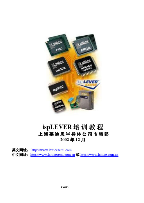
一、新建工程并加载程序文件1.1启动ispLEVER,选择File—New Project,在弹出的Project Wizard对话框中填写或选择Project Name、Location、Design Entry Type、Synthesis Tools、Simulator Tools,点击“下一步”。
我们给出一个例子,osc_led,见图1.1。
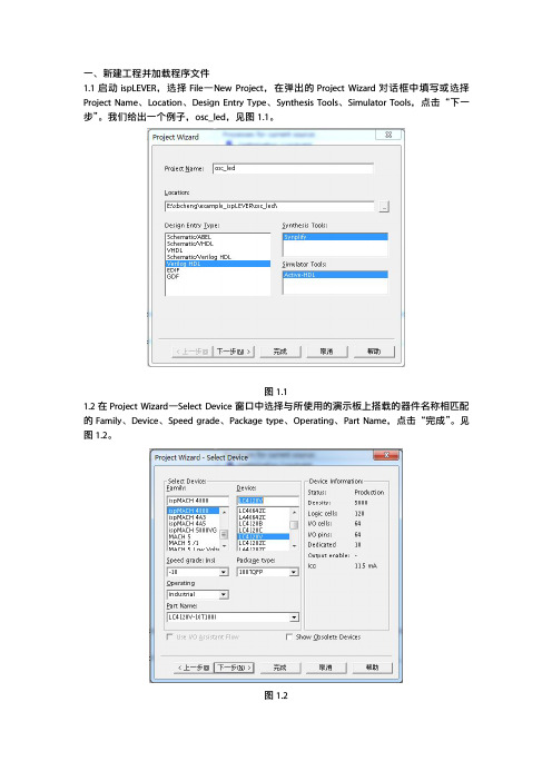
图1.11.2在Project Wizard—Select Device窗口中选择与所使用的演示板上搭载的器件名称相匹配的Family、Device、Speed grade、Package type、Operating、Part Name,点击“完成”。
见图1.2。
图1.21.3在ispLEVER软件的Source in Project窗口中,会出现新建的工程名称和选择的器件名称,见图1.3,工程名称:osc_led,选择的器件名称:LC4128V-10T1001。
图1.31.4加载程序文件有两种方法可以加载程序文件,一种是直接调用现有的程序文件,另一种是直接编写程序文件。
1.4.1调用现有的程序文件。
1.4.1.1在1.3中选择的器件名称LC4128V-10T1001上右击鼠标,选择Import,在弹出的对话框中选择现有的程序文件,点击打开。
见图1.4.1.1。
图1.4.1.11.4.1.2在弹出的Import Source Type对话框中选择Type of Source,源文件选择Verilog Module,点击OK。
见图1.4.1.2。
图1.4.1.21.4.1.3加载测试文件,方法同上面源文件的加载,区别是在选择source type时要选择“Verilog Test Fixture”,在弹出的“Associate Verilog Test Fixture”对话框中要选择器件名,如图1.4.1.3A、B、C所示:ABC图14.1.31.4.2直接编写程序文件。
ispLEVER使用说明

第一节 ispLEVER开发工具的原理图输入启动ispLEVER(按Start=>Programs=>Lattice Semiconductor=>ispLEVER菜单)一、创建一个新的设计项目A.选择菜单File。
B.选择New Project...。
选择D盘(数据盘,未保护,可保存),创建新文件夹,重命名为TEST。
进入文件夹,PROJECT命名为ADD1.SYN,保存类型为SYN,PROJECTTYPE选择第一项SCHEMATIC/ABEL,保存即可。
C.你可以看到默认的项目名和器件型号: Untitled andispLSI5256VE-165LF256。
二、项目命名D.用鼠标双击Untitled。
E.在Title文本框中输入“test”,并选OK(此操作可选)。
三、选择器件a)双击ispLSI5256VE-165LF256, 你会看到Device Selector对话框(如下图所示)。
b)方法一:在Select Device窗口中选择:Family中选择 ispLSI 1K Device;Device 中选择ispLSI1032E;Speed grade中选择70; Package中选择 84PLCC;Operating 中选择Industrial。
方法二:按动器件目录中(Part)的滚动条,直到找到并选中器件1032E-70LJ84I。
c)揿OK按钮,选择这个器件。
d)在软件弹出的如下图显示的ispLEVER Project Navigator窗口中,按否(N)按钮。
e)在软件弹出的如下图显示的Confirm Change窗口中,按Yes按钮。
f)因改选器件型号后,先前的约束条件可能对新器件无效,因此在软件接着弹出的如下图显示的ispLEVER Project Navigator窗口中,按Yes按钮,以用来去除原有的约束条件。
四、在设计中增加源文件一个设计项目由一个或多个源文件组成。
海洛斯操作手册(说明书)

HIROSS恒温恒湿机房精密空调操作手册HIMOD系列北京****科技有限公司技术部2009年01月01日目录第一章HIMOD系列海洛斯空调概述 (2)型号多 (3)控制技术先进 (3)制冷系统 (3)送风系统 (3)加湿系统 (3)加热系统 (4)1.7其它 (4)第二章HIMOD系列海洛斯空调型号含义 (4)第三章有关空调的一些资料 (5)气流组织方式(详见下图) (5)盖板纽开启方式(详见下图) (5)空调重量(单位:Kg) (5)机组尺寸及维护空间 (6)第四章制冷循环管路示意图 (7)风冷却(A型) (7)水冷却(W型) (8)双冷源(D型) (9)单系统(C型) (10)双系统(C型) (10)第五章调速风机调速接线示意图 (11)第六章MICROF ACE概述 (12)概述 (12)面板简介液晶显示屏 (13)液晶显示屏介绍 (13)第七章MICROF ACE面板的操作 (13)第八章控制器的使用 (14)控制器(HIROMATIC)概述 (14)控制器的操作 (15)菜单结构 (17)第九章日常维护及特殊维护 (18)日常维护 (18)特殊维护 (19)第十章常见报警及处理 (20)低压报警 (20)高压报警 (21)加湿报警 (21)失风报警 (21)电加热过热报警 (22)显示器发黑 (22)空调不制冷 (22)附录1:参数列表 (22)附录2:报警内容列表 (26)附录3:各菜单项含义: (28)第一章HIMOD系列海洛斯空调概述HIMOD系列海洛斯空调(HIMOD空调)是当今世界上最先进的机房专用恒温恒湿机房专用精密空调。
随着IT业的突飞猛进的发展,各种布局、面积差别很大的机房如雨后春笋般纷纷出现了,使用环境也不一而同。
为适应各种不同要求的机房,新开发的海洛斯HIMOD系列空调应运而生。
她是在保留她的前一代产品HIRANGE系列机房空调的优点,又应用了当今世界上提高了的制冷技术及制冷部件制造工艺,使用当今最先进的模块化设计理念生产出来的高科技机房空调产品。
2024年度LatticeispLEVER使用教程

丰富的仿真验证
支持功能仿真和时序仿真,可 对设计进行全面的验证和调试 。
全面的设计输入支持
支持原理图、Verilog/VHDL 硬件描述语言等多种设计输入 方式。
2024/3/23
灵活的布局布线
提供手动和自动布局布线功能 ,支持用户自定义布局和布线 策略。
广泛的IP核库
集成了多种常用的IP核,如计 数器、FIFO、UART等,方便 用户快速构建系统。
2024/3/23
元器件库导入与导出
支持导入和导出元器件库,方便不 同项目之间的共享和复用。
元器件搜索与筛选
提供强大的搜索和筛选功能,可快 速找到所需元器件。
21
06
仿真与验证功能应用
2024/3/23
22
仿真设置与运行
01
创建仿真工程
在LatticeispLEVER中,首先需 要创建一个新的仿真工程,指
定工程名称和存储路径。
02
添加设计文件
将待仿真的设计文件(如 VHDL、Verilog代码文件)添
加到工程中。
03
配置仿真参数
根据设计需求,配置仿真参数 ,如仿真时间、输入激励等。
04
运行仿真
设置好仿真参数后,可以运行 仿真,观察设计的行为和功能
。
2024/3/23
23
波形显示与分析
2024/3/23
2024/3/23
丰富的元器件符号库
提供大量常用的元器件符号,方便用户快速 搭建电路。
原理图自动检查功能
可检查原理图的正确性,如元器件连接是否 正确、导线是否短路等。
19
PCB设计
PCB板层管理
支持多层PCB板设计,可自定义各层属性 和参数。
ispLEVER官方中文培训教程

目录第一节ispLEVER 简介第二节ispLEVER 开发工具的FPGA设计输入方法第三节ModelSim 的使用方法第四节设计的实现第一节 ispLEVER简介ispLEVER 是完整的CPLD和FPGA设计软件,能帮助用户完成从概念到完成产品的设计。
ispLEVER包含许多有力的开发的工具,用于设计输入、项目管理、IP集成、器件映射、布局和布线,以及在系统逻辑分析等。
ispLEVER (Windows) 还包含业界领头羊——我们的伙伴Synplicity 和Mentor Graphics ——的第三方工具,这些工具用于综合和仿真。
ispLEVER 6.0完全支持最新的高性能、低成本的90纳米LatticeECP2™和LatticeSC™ 终极性能的系统芯片FPGA系列,并且具有引以为豪的空前性能和经过重大改进的设计流程。
ispLEVER 6.0版的主要亮点包括:支持业界最快的90纳米FPGA;推出新的、高度集成的Design Planner接口、针对原理图FPGA设计支持的改进以及一个IPexpress™ 用户可配置的IP核拓展库。
ispLEVER设计流程如下:软件主要特征:1. 输入方式* 原理图输入* ABEL-HDL输入* VHDL输入* Verilog-HDL输入* EDIF输入* 原理图和硬件描述语言混合输入2.逻辑模拟* 功能模拟* 时序模拟3.编译器* 结构综合、映射、自动布局和布线4.支持的器件* 含有支持ispLSI器件的宏库及MACH器件的宏库、TTL库* 支持所有LatticeEC、LatticeECP、LatticeSC、LatticeXP、ispLSI、ispMACH、ispGDX、GAL、MachXO、ORCA FPGA/FPSC、ispXPGA和ispXPLD 器件5. 工具* Design Planner、EPIC Device Editor、IPexpress、ispTRACY Core Linker、ispVM、ispTRACY Logic Analyzer、Power Calculator、Block Modular Design Wizard、Memory Initialization Tool、Synplify Synthesis、Precisin Synthesis、ModelSim Simulator和TCL等。
- 1、下载文档前请自行甄别文档内容的完整性,平台不提供额外的编辑、内容补充、找答案等附加服务。
- 2、"仅部分预览"的文档,不可在线预览部分如存在完整性等问题,可反馈申请退款(可完整预览的文档不适用该条件!)。
- 3、如文档侵犯您的权益,请联系客服反馈,我们会尽快为您处理(人工客服工作时间:9:00-18:30)。
FPGA Design withispLEVER Tutorial Lattice Semiconductor Corporation5555 NE Moore CourtHillsboro, OR 97124(503) 268-8000September 2008CopyrightCopyright © 2008 Lattice Semiconductor Corporation.This document may not, in whole or part, be copied, photocopied, reproduced, translated, or reduced to any electronic medium or machine-readable form without prior written consent from Lattice Semiconductor Corporation.TrademarksLattice Semiconductor Corporation, L Lattice Semiconductor Corporation (logo), L (stylized), L (design), Lattice (design), LSC, E2CMOS, Extreme Performance, FlashBAK, flexiFlash, flexiMAC, flexiPCS, FreedomChip, GAL, GDX, Generic Array Logic, HDL Explorer, IPexpress, ISP, ispATE, ispClock, ispDOWNLOAD, ispGAL, ispGDS, ispGDX, ispGDXV, ispGDX2, ispGENERATOR, ispJTAG, ispLEVER, ispLeverCORE, ispLSI, ispMACH, ispPAC, ispTRACY, ispTURBO, ispVIRTUAL MACHINE, ispVM, ispXP, ispXPGA, ispXPLD, LatticeEC, LatticeECP, LatticeECP-DSP, LatticeECP2, LatticeECP2M, LatticeMico8, LatticeMico32, LatticeSC, LatticeSCM, LatticeXP, LatticeXP2, MACH, MachXO, MACO, ORCA, PAC, PAC-Designer, PAL, Performance Analyst, PURESPEED, Reveal, Silicon Forest, Speedlocked, Speed Locking, SuperBIG, SuperCOOL, SuperFAST, SuperWIDE, sysCLOCK, sysCONFIG, sysDSP, sysHSI, sysI/O, sysMEM, The Simple Machine for Complex Design, TransFR, UltraMOS, and specific product designations are either registered trademarks or trademarks of Lattice Semiconductor Corporation or its subsidiaries in the United States and/or other countries. ISP, Bringing the Best Together, and More of the Best are service marks of Lattice Semiconductor Corporation.HyperTransport is a licensed trademark of the HyperTransport Technology Consortium in the U.S. and other jurisdictions.Other product names used in this publication are for identification purposes only and may be trademarks of their respective companies.DisclaimersNO WARRANTIES: THE INFORMATION PROVIDED IN THIS DOCUMENT IS “AS IS” WITHOUT ANY EXPRESS OR IMPLIED WARRANTY OF ANY KIND INCLUDING WARRANTIES OF ACCURACY, COMPLETENESS, MERCHANTABILITY, NONINFRINGEMENT OF INTELLECTUAL PROPERTY, OR FITNESS FOR ANY PARTICULAR PURPOSE. IN NO EVENT WILL LATTICE SEMICONDUCTOR CORPORATION (LSC) OR ITS SUPPLIERS BE LIABLE FOR ANY DAMAGES WHATSOEVER (WHETHER DIRECT, INDIRECT, SPECIAL, INCIDENTAL, OR CONSEQUENTIAL, INCLUDING, WITHOUT LIMITATION, DAMAGES FOR LOSS OF PROFITS, BUSINESS INTERRUPTION, OR LOSS OF INFORMATION) ARISING OUT OF THE USE OF OR INABILITY TO USE THE INFORMATION PROVIDED IN THIS DOCUMENT, EVEN IF LSC HAS BEEN ADVISED OF THE POSSIBILITY OF SUCH DAMAGES. BECAUSE SOME JURISDICTIONS PROHIBIT THE EXCLUSION OR LIMITATION OF CERTAIN LIABILITY, SOME OF THE ABOVE LIMITATIONS MAY NOT APPLY TO YOU.LSC may make changes to these materials, specifications, or information, or to the products described herein, at any time without notice. LSC makes no commitment to update this documentation. LSC reserves the right to discontinue any product or service without notice and assumes no obligationto correct any errors contained herein or to advise any user of this documentof any correction if such be made. LSC recommends its customers obtain thelatest version of the relevant information to establish, before ordering, that theinformation being relied upon is current.Type Conventions Used in This DocumentConvention Meaning or UseBold Items in the user interface that you select or click. Text that you typeinto the user interface.<Italic>Variables in commands, code syntax, and path names.Ctrl+L Press the two keys at the same time.CourierCode examples. Messages, reports, and prompts from the software....Omitted material in a line of code....Omitted lines in code and report examples.[ ]Optional items in syntax descriptions. In bus specifications, thebrackets are required.( )Grouped items in syntax descriptions.{ }Repeatable items in syntax descriptions.| A choice between items in syntax descriptions.斜体描述ContentsIntroduction1Learning Objectives1Time to Complete This Tutorial2System Requirements2Accessing Online Help2About the Tutorial Design2About the Tutorial Data Flow3Restore the Tutorial Files4Task 1: Create a New Verilog or VHDL Project5Create a New Project5View Project Source File9Adjust Tool and Environment Options9Task 2: Assign Location and Timing Preferences11Assign Pin Location Preferences11Assign Timing Preferences15Task 3: Design Synthesis and Mapping19View the Mapping Results19View the Static Timing Analysis Report20Task 4: Place, Route, and Post-Route Timing20Place and Route the Design21View the Static Timing Analysis Report23Task 5: Viewing the Device Implementation24View the Device Implementation After Placement and Routing24 Find the Critical Path24Examine Programming of Design Planner Elements28Examine the Counter Implementation in Slices30Task 6: Improving PAR Results – Part 133Improving PAR Results for Verilog33ContentsImproving PAR Results for VHDL34Viewing the TRACE Reports34Task 7: Generate a Module Using IPexpress35Generate a sysCLOCK PLL Module36Add a PLL Instance39Examine Timing Results with sysCLOCK PLL42Task 8: Improving PAR Results – Part 243Add a Delay Adjustment Factor44Perform Placement and Routing45Guide Component Placement46Task 9: Examining Device Utilization48View the Device Implementation48View the Routing Congestion48Task 10: Estimating Power Consumption51Estimate Power for Routed Design51Estimate Power for a Different Temperature53Estimate Power for a Different Device53Task 11: Simulating the Design54Start Functional Simulation57Start Timing Simulation58Summary58Glossary58Recommended Reference Materials60FPGA Design withispLEVER TutorialIntroductionThis tutorial is intended for a new user or a user who uses ispLEVERinfrequently. It shows you how to use several processes, tools, and reportsfrom the ispLEVER software suite to implement a simple (RTL) Verilog or实现VHDL design in a LatticeEC family device. You will prepare the design forsimulation, power estimation, static timing analysis, and timing-drivenplacement and routing, reviewing output reports as you make progress. Youwill constrain the design’s inputs and outputs to meet the signal type andlocation requirements of your system-level design. You will modify andconstrain the design to leverage the architectural resources of the LatticeECdevice to give you a high-performance implementation. The tutorial covers themost common procedure and software options, so you will have a base ofunderstanding before you tackle larger or more timing-critical designs thatmay require more refinement and control to meet your performance andutilization objectives.Learning ObjectivesWhen you have completed this tutorial, you should be able to do the following:Use ispLEVER to create a new Verilog HDL or VHDL project, target adevice, and add a Verilog HDL or VHDL source file to the project usingProject Navigator.Generate a sysCLOCK PLL module, add it to your project, and refer to itfrom your source using IPexpress and Text Editor.Lock signals to device package pins and define a period or frequency andclock-to-out timing constraints using Design Planner.Implement the design using the mapping, placing, and routing processesand view the resulting reports using Project Navigator.Interpret the static timing analysis report and adjust the design to meetyour timing objectives. Modify and constrain the design to meet your performance objectives.View the device implementation and review the relative routing congestion and programmable functional unit (PFU) utilization using Design Planner.Estimate power consumption using Power Calculator. Prepare the design for simulation.Time to Complete This Tutorial The time to complete this tutorial is about two and a half hours.System Requirements One of the following software configurations is required to complete the tutorial:ispLEVERispLEVER Pro ispLEVER StarterAccessing Online HelpYou can find online help information on any tool included in the tutorial at anytime by pressing the F1 key.About the Tutorial Design The tutorial design begins with a simple counter described with register-transfer-level (RTL) Verilog or VHDL that you might find in any Verilog orVHDL textbook. It evolves into a more sophisticated version that uses registered outputs and a phase-locked loop to help reconcile the internal timing of the FPGA with the external specifications. The design is modified and constrained to account for the f MAX switching characteristics of theLatticeEC device (programmable function units (PFUs) as compared toprogrammable interface cells (PICs)) and special features like the sysCLOCKPLL to leverage the feedback compensation of the internal VCO to reduceclock-to-output delay (t CO ).You can perform the tutorial with either a Verilog HDL or VHDL source file.The complete tutorial design is composed of two Verilog or VHDL modules: a16-bit up counter with an active-low asynchronous reset and a PLL. Figure 1illustrates versions A through C of the tutorial design and the resulting timingcharacteristics. The counter is described with register-transfer-level (RTL)Verilog or VHDL and a structural model produced by an ispLEVER applicationcalled IPexpress, which describes the PLL module. The counter’s 250-MHzclock is driven externally in versions A and B of the design. In version C, it is produced by a sysCLOCK PLL that is introduced to effectively remove fromthe critical path timing equation the route delay introduced by the clock tree,allowing easier timing analysis at the PC board.说明拥挤消耗功率计算器RTL 描述复杂的使一致规格外部的Figure 1: Tutorial DesignAbout the Tutorial Data FlowA few key processes of the ispLEVER Project Navigator are used to transformthe Verilog or VHDL source code of the tutorial design into LatticeSemiconductor databases that are used by the software system to implementand analyze the logic. Figure 2 illustrates the tutorial data flow through thesystem. You may find it helpful to refer to this diagram as you move throughthe tutorial tasks.NoteIn this tutorial, where the step to be performed depends on the type of source file youare using, the step is prefaced by “Verilog:” or “VHDL:.” Where a sequence of stepsdiverge for Verilog or VHDL, they are grouped by headings that indicate their application to Verilog or VHDL.指出有少数一些按键是 将源代码转换成Lattice 半导体的数据资料丆用来 通过软件实现和 分析逻辑Figure 2: Tutorial Design Flow Restore the Tutorial FilesIf this tutorial has been previously run on your system, use the followingprocedure to restore the original tutorial files.To restore the original tutorial files:pinassign_pll_a.v (or pinassign_pll_a.vhd )IPexpress pinassign_pll.v or pinassign_pll.vhd Build Database Map DesignMap TRACE Report/Place& Route TRACE Reportec_pll.v or ec_pll.vhd pinassign_pll.prf Place & Route Design pinassign_pll.ncdpinassign_pll.ngd pinassign_pll.tw1pinassign_pll twr设计流程图Task 1: Create a New Verilog or VHDL ProjectIn this task, you will create a new Verilog HDL- or VHDL-type project andprovide it with a simple title using Project Navigator. To begin a new project,you give the project file (.syn) a name and declare the project type. TheispLEVER software saves an initial design file with the .syn file extension inthe directory that you specify. All project files are typically created in this指定directory, but you can reference source files from outside of it. The projecttype specifies that all design sources will be of this type.Create a New ProjectIf you want to preserve the original tutorial files, save the fpga_design_tutordirectory to another location on your computer before proceeding.To create a new project:1.Start Project Navigator if it is not already running.2.In Project Navigator, choose File > New Project to open the ProjectWizard dialog box.3.In the Project Wizard dialog box, shown in Figure3, do the following:a.In the Project Name box, type pinassign_PLL.b.In the Location box, specify the following directory:<install_path>\examples\Tutorial\fpga_design_tutorc.In the Design Entry Type box, choose Verilog HDL or VHDL.d.In the Synthesis Tools box, choose Synplify.e.In the Simulator Tools box, choose your preferred simulator.f.Click Next.Figure 3: Project Wizard Dialog Box4.In the Project Wizard – Select Device dialog box, shown in Figure 4, dothe following:a.In the Family box, choose LatticeEC .b.In the Device box, choose LFEC1E .c.In the Speed Grade box, choose -3.d.In the Package Type box, choose TQFP100.e.In the Operating Conditions box, choose Commercial .f.Click Next to open the Project Wizard – Add Source dialog box.5.In the Project Wizard – Add Source dialog box, click Add Source toactivate the Import File dialog box.6.Select pinassign_pll.v (or pinassign_pll.vhd ) and click the Open buttonto open the Import Source Type dialog box, shown in Figure 5.7.Select Verilog Module (or VHDL Module ) and click OK .Figure 4: Project Wizard – Select a Device Dialog BoxFigure 5: Import Source Type Dialog BoxThe file is added to the source file list in the Project Wizard – Add Sourcedialog box, as shown in Figure 6.8.Click Next .9.In the Project Wizard – Project Information dialog box, shown in Figure 7,click Finish .The new project is created, and the source file is referenced in theSources in Project list, as shown in Figure 8. Click on the part name to seethe contents of the Processes for Current Source window.Figure 6: Project Wizard – Add Source Dialog BoxFigure 7: Project Wizard – Project Information Dialog Box10.The Sources Window provides two tabs to organize the design modulesand files related to the project. The Modules tab displays each unique module and related filename used in the design hierarchy. A text entry box and magnifying glass icon allows you to search the module list.In the Sources Window, click the Files tab. Project comments and source files related to the project appear. Folders such as Documents, Stimulus Files and Input Files help organize files. Project Navigator automatically compiles all HDL source files of the project to create the module hierarchy and an ordered file list for simulation and synthesis tools. If syntax faults occur or the top of design is ambiguous you may be prompted to specify the top. File order can be adjusted in those cases where automaticordering does not work correctly.11.In the Sources in Project window, double-click the project title,pinassign_PLL, to open the Project Properties dialog box.The default title for a new project is the project name that you initiated instep 3. You can create another title for the project with as many charactersas you want. The title can contain spaces and any other keyboardcharacters, except tabs and returns.12.In the Title text box, type Pin assign and PLL sample and click OK.Figure 8: Project Navigator Window Showing New ProjectNoteYou can target a design to another Lattice Semiconductor device later, if you want. Forexample, you may discover that you can target a smaller, less expensive devicepackage if your design will fit, or you may decide to migrate an existing project to anew device family. To select a new device, choose Source > Select New Device.两个标签模块等级安排好你也可以创建另一个标题给这个工程很多人都这样做标题可以包含其他的字符丆制表符除外View Project Source FileYou “describe” a project by specifying the source files that represent the design. You can either import an existing source or create a new one. The source files for the project appear in hierarchical and alphabetical order within the Sources in Project window, Modules tab, by module name. If your source file contains more than one module, it will appear in the list as many times as there are module instantiations, using the style:module_name (source_filename)To view a source file of the project:1.Click the Modules tab in the Sources in Project window.2.Double-click the pinassign_PLL module to open the source file in TextEditor, as shown in Figure9.Figure 9: Source File in Text Editor3.Choose File > Exit to exit Text Editor.Adjust Tool and Environment OptionsTiming checkpoints occur after both the mapping and the placement and routing stages of the process flow to flag excessive delay conditions. In this tutorial, you will set checkpoints that will report if a check fails, but not block forward progress.To adjust tool and environment options:1.Choose Tools > Timing Checkpoint Options to bring up the TimingCheckpoint Options dialog box, shown in Figure10.2.In this dialog box, select the following:a.In the Checkpoint Options section of the Before Route field, set If Checkpoint failed to Continue .b.In the Checkpoint Options section of the After Route field, set IfCheckpoint fails to Continue .c.Click OK .3.Choose Options > Environment to open the Environment Options dialogbox, shown in Figure 11. In this dialog box, do the following:a.Click the Log tab.b.Turn off Using Web Browser .c.Click the Revision Control tab.d.Select Close Window when Revision Control is Disabled .e.Click OK .4.If the Revision Control window at the right of Project Navigator is open,right-click in it and choose Turn Off from the pop-up menu.The revision control window closes. This tutorial will not use projectrevision control.To re-open the Revision Control window, click on the Revision Controlicon in the Project Navigator toolbar.Figure 10: Timing Checkpoint Options Dialog Box布线 领域Task 2: Assign Location and Timing PreferencesIn this task, you lock signals to device package pins and define period or frequency and clock-to-out timing constraints. You use Design Planner, agraphical interface to the logical preference file (<project_name >.lpf), tocreate timing and location constraints for ispLEVER. The logical preferencefile is interpreted by the design mapper (Map Design process) to produce aphysical preference file (<project_name >.prf) for the place-and-route system.Now that the logic design has been captured, you can create constraints that will guide the placement and routing process to locate signals at specificpackage pin locations and implement the logic and routing to meet yourdesign’s performance objectives.Assign Pin Location PreferencesIn Project Navigator, select the LFEC1E-3T100C device in the Sources inProject window.and translates the synthesis output in EDIF to an NGD Logical Designdatabase. Information and warning messages appear in the AutomakeLog tab of the output panel of Project Navigator. You can ignore these warnings in this tutorial.The Spreadsheet View, Package View, and Design Planner Controlwindows now appear.If it is not already selected, select the Port Attributes tab in theSpreadsheet View.Figure 11: Environment Options周期或者频率约束面板The Spreadsheet View displays the Port Attributes tab for assignmentsrelated to location and buffer configuration. Preferences such as pinlocation, I/O type, and slew rate appear as columns in the sheet. It iscommon to use the Logic Signal Connections section of the device datasheet as a reference to type in pin locations.4.Click anywhere on the Spreadsheet View and verify that the View > ShowDefault Value option is selected.The Package View window provides a graphical representation of the100-pin TQFP device package.In the next steps, you will drag and drop external signals to pin locations inthe Package View window.5.Double-click the title bar of the Package View window to enlarge the view.6.Click anywhere in the right pane of the Package View window and chooseView > Top View .The Package View window adjusts to display the device package asviewed from above.7.Click on the + next to Device and next to Design Signals, then click on the+ next to all pins under Device to expand the list of pins.a.Find pin 99 in the expanded tree.b.Highlight pin 99 and right-click.c.Select Locate Device Pin .The Package View expands the view and highlights pin 99.8.Click on + to expand the CNT[15:0] bus in the left pane, as shown inFigure 12.NoteThe menu items of the Spreadsheet View are context-sensitive and enablefunctions only if they apply to the window or pane that is selected. If a menu item isunexpectedly unavailable, click on the pane to which the function applies.NoteYou can display the name of each pad by positioning the cursor over the pad.核实丆查证敏感的如果一个菜单项是不能用的点击那个函数申请的窗口9.Drag and drop the CNT[15:0] bus onto device pin 99.Design Planner fills the top left I/O bank (Bank 0) and a portion of the topright bank (Bank 1). The colored outlines of the pads represent banks.RESET_L, pin 3 (global reset) CLK, pin 19 (one of two reference clock pins for the LFEC1, 100-pinTQFP sysCLOCK PLL, which will be added later in the tutorial)As you assign pins, the package view is colored yellow to indicate outputtype ports, and the pin number appears next to the user signal in the leftpane of the Package View pane. The blue color represents inputs.Figure 12: List of Signals in BusNoteBe sure that you place the arrow connected to the bus squarely onto thedevice.衬底特殊作业光标The Spreadsheet View is also updated with the assignments that youhave made. The Pin column of the Port Attributes tab displays the pinnumbers assigned to each user signal.11.Click on the Spreadsheet View and choose Tools > PIOS DRC.12.Click OK in the Design Planner - Information pop-up message box thatcontains the following line:PIO DRC checks: No errors detected.The results of the PIO design rule check appear in the Design PlannerControl window. They help to ensure that the assignments that you havemade are legal before you submit the design to the mapping, placement,and routing tools later.13.In the Spreadsheet View, choose File > Save to update pinassign_pll.lpf.Figure13 shows the pin assignments in the Spreadsheet View.Figure 13: Pin Assignments in the Spreadsheet View专业的工具This task provides a preview of the many logical and physical preferences available for constraining FPGA mapping, placement, and routing. The FPGA Preference Language is explained in detail in the online help.To assign timing preferences with the Design Planner:1.Maximize the Spreadsheet View by double-clicking on the title bar, andchoose Preference > Period/Frequency to open the PERIOD/FREQUENCY Preference dialog box, shown in Figure14.In the Type field of the dialog box, select FREQUENCY.b.In the Second Type field, select Clock Port.A list of clock ports appears in the Available Clock Ports list.c.In the Frequency box, type 250.d.Select CLK in the Available Clock Ports box.e.Click Add.f.Click OK to close the dialog box.Figure 14: PERIOD/FREQUENCY Preference Dialog BoxThe new preference appears in the Period/Frequency tab of theSpreadsheet View, as shown in Figure 15.The FREQUENCY preference identifies the minimum operating frequencyfor all sequential-output-to-sequential-input pins clocked by the specified net.2.Choose Preference > Input_setup/Clock_to_out to open theINPUT_SETUP / CLOCK_TO_OUT Preference dialog box, shown inFigure 16.a.In the Type field of the dialog box, select CLOCK_TO_OUT .A list of signal names appears as the Clock Out Ports list.b.In the Second Type field, choose All Ports .c.In the Time box, enter 4.0 ns.d.In the Clock Ports/Nets box, select CLK .e.Click Add . Figure 15: Frequency Preference Set in Spreadsheet View这个频率参数 识别最小的工作频率对于连续输出和 连续输入 引脚f.Click OK to close the dialog box.Figure 16: INPUT_SETUP/CLOCK_TO_OUT Preference Dialog BoxThe new preference appears in the In/Out Clock tab of the SpreadsheetView, as shown in Figure17.Figure 17: Clock-to-Out Preference Set in In/Out Clock Tab of Spreadsheet Viewclock的最大允许输出延时The CLOCK_TO_OUT preference specifies a maximum allowable outputdelay relative to a clock. For example, the delay from CLK to theb.In the Filter box, type R*, and click Go .Those nets that begin with “R” appear in the Available Nets list.c.Select RESET_L_c .d.Click Add .e.Click OKto close the dialog box.The new preference appears in the Block tab of the Spreadsheet View, asshown in Figure 19.The BLOCK preference blocks timing analysis on nets, paths, buses, orcomponent pins that are irrelevant to the timing of the design. In this example, RESET_L_c drives the global set/reset (GSR) line that servesFigure 18: Block Preference Dialog BoxFigure 19: Block Preference Set in Block Tab of Spreadsheet ViewBLOCK 参数 全程时间分析 在 网络丆路径丆总线和 器件管脚与设计不相关的 时间FPGA Design with ispLEVER Tutorial Task 3: Design Synthesis and Mappingas the counter’s asynchronous reset. You can safely ignore it duringtiming analysis.4.Choose File > Save to update pinassign_pll.lpf.5.Choose File > Exit in the Design Planner Control window to exit theDesign Planner.Task 3: Design Synthesis and Mapping In this task, you will review the report created by the mapping process, which converts a logical design represented as a network of device-independent components (for example, gates and flip-flops) produced by logic synthesisand the Build Database process into a network of device-specific components(for example, PFU/PFF, IOLOGIC, or EBR) that will be eventuallyimplemented by the placement and routing process.After mapping is complete, you can perform static timing analysis to confirmthat the current implementation, accounting only for logic element delays, willmeet the timing constraints that you specified earlier.View the Mapping ResultsTo view the mapping results:1.In Project Navigator, select the LFEC1E-3T100C device in the Sources inProject window.2.Double-click Map Report .After a few moments, the pinassign_pll.mrp tab appears in the outputpanel.3.Review the major sections of the report:Design Information: Command line, device, and software versionNoteFor more information on setting preferences, select the Setting Preferences topicin the online help.NoteNotice the <port_name >_c net names created by the Synplify synthesis process for the clock tree and GSR nets. These internal signals are driven through buffersinferred by logic synthesis. In some cases, timing and location preferences refer tothese internal names instead of the external port name associated with an I/Obuffer pad. You may need to inspect the Map report or the output EDIF netlist ofthe Build Database process to understand what nets your synthesis tool produced.NoteClick on a tab to view it. If you do not see a tab, drag the vertical splitter bar to theright.注意丗端口名是被 Synplify 综合进程对时钟树和 GSR 网络综合产生的综合和 映射把逻辑设计转换为独立的器件网表仅仅是 器件 延时。