基于NAND Flash的FFS设计与实现
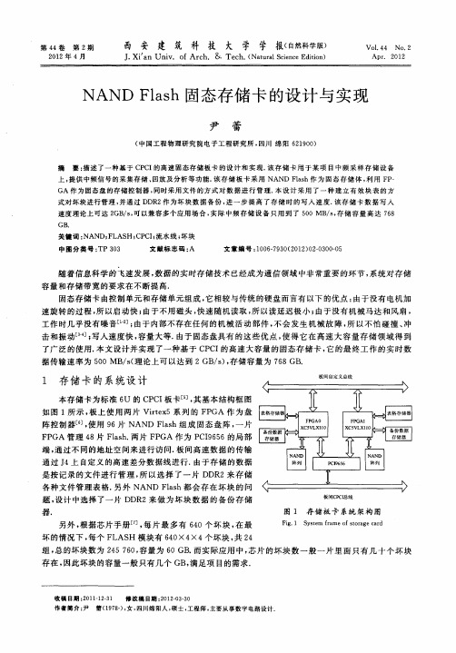
NAND Flash固态存储卡的设计与实现
收 稿 日期 :0 11—1 2 1—23
修 改稿 日期 :0 20 —0 2 1 -33
作者简介 : 尹
营( 98) 女 , 17 一 , 四川绵阳人 , 硕士 , 工程师 , 主要从事数字 电路设计
第 2期
尹
蕾: NAN ls D Fah固态存储 卡的设计 与实现
31 O
该存 储卡 用 于 高 速采 样 存 储
系统 , 要求 写 入速 度 快 、 储 容 量 存
大. 统 选 用 的 NAND Fa h芯 系 ls 片 为 三 星 的 K9 G0 U5 , NC 8 M 该
Fah芯 片 单 片 的 容 量 为 8 GB ls . 该 Fah的基本 结 构 为 : ls 4个 de i,
每个 de 含 81 2块 , i包 9 每块 包 含
容 量 和存储带 宽 的要求 在不断 提高 .
固态存储 卡 由控制 单元 和存储 单元组 成 , 相较 与传统 的硬 盘而 言有 以下 的优点 : 它 由于没有 电机加 速旋转 的过 程 , 以启 动快 ; 所 由于 不用磁头 , 快速 随 机读取 , 以读延迟 极小 ; 所 由于没有 机械 马达 和风扇 ,
A pr 2 2 . 01
21 0 2年 4月
NAND F ah固态 存储 卡 的设 计 与实 现 ls
尹 蕾
( 国 工程 物 理 研 究 院 电子 工 程 研 究 所 , 川 绵 阳 6 10 ) 中 四 2 9 0
摘 要 : 述 了 一 种 基 于 C C 的高 速 固 态 存 储 板 卡 的设 计 和 实 现. 存 储 卡 用 于 某 项 目中 频 采 样 存 储 设 备 描 PI 该
据传输 速率 为 5 0MB s 理论上 可 以达到 2G / ) 存储 容量 为 7 8G . 0 / ( B s, 6 B
基于NAND Flash的数据存储系统设计
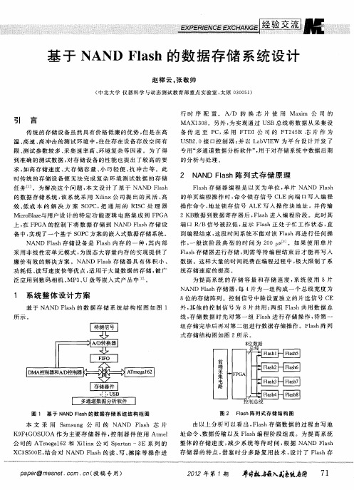
时 , 1片 Fah的 编 程 已经 完 成 , 于 准 备 就 绪 状 态 , 第 l s 处 可 以 写 入 新 的 数 据 , 此 可 以 等 效 为 Fah存 储 器 的 编 程 时 由 ls
间为 0 。这 样 就 可 以实 现 F a h阵 列 的 连 续 传 输 数 据 , ls 提 高 系 统 的 整 体 速 度 ] 。
r o 币. 0 I 7 . l F
卜 GDW E撑o X30 簪 RN 1 C 5E N P TS兰 T_ S0
图 4 U SB接 口 电 路 图
程状 态 时 , 对 第 3片进 行 数 据 加 载 操 作 ; 次 执 行 下 去 , 再 依
待 一 次 整 体 操 作 完 成 后 4片 F ah都 已加 载 完 数 据 。此 ls
21年第7 平 机 嵌 条毛 用 7 0 2 期 入式 ' 1 应
经 验 交 流
储阵 列 , 即利 用 上 一 片 F ah的 编 程 时 间 对 下 一 片 F a h ls ls
..
j
主 机 通 信 以 及 数 据 的 传 输 。US B芯 片使 用 由 F D 司 T I
外 , 他 的控 制 信 号 为 8片 共 用 ; 组 F a h共 用 数 据 总 其 两 ls
线 , 储 数 据 时 先 对 第 一 组 Fah进 行 存 储 操 作 , 第 一 存 ls 待 组 存 储 完 毕 后 再 对 第 二 组 进 行 数 据 存 储 操 作 。Fah阵列 ls 式 存 储 结 构 图如 图 2 示 。 所
廉 价 有 效 的解 决 方 案 。NAND ls F a h存 储 器 具 有 体 积 小 、 功 耗 低 、 写 速 度 快 等 优 点 , 用 于 大 量 数 据 的 存 储 , 广 读 适 被
NANDFlash阵列存储系统中FTL的设计与实现
摘要近年来,随着技术的进步,NAND Flash型闪存已逐渐褪去其以往高价的形象,在轻巧度、可靠度以及容量上不断地提升,加上其低功耗、掉电非易失等特点,已被广泛应用于各种移动设备及嵌入式存储系统中。
以NAND Flash作为存储介质的固态硬盘(SSD),由于具有普通的磁介质硬盘(HDD)所不能比拟的优点,在近些年来迅速成为存储领域的热点技术。
然而,一个典型的NAND Flash器件是由若干个块(block)组成,而每块又包含若干页(page),其特殊的物理结构使NAND Flash无法像磁介质硬盘一样原地更新数据,因此,需要在文件系统及物理层之间加入闪存转换层(FTL),解决文件系统的逻辑扇区地址与NAND Flash物理页地址的映射问题。
本文提出并实现了一套基于NAND Flash阵列存储系统中FTL的设计算法,包含地址映射、坏块管理,主要完成的工作如下:[1].构建地址映射对于逻辑地址到物理地址的映射,实现了一种基于LOG BLOCK的混合映射机制,可以有效的避免不必要的拷贝与擦除操作,做到实时更新映射表,节约映射时间,且同时减小了映射表占有的空间大小。
[2].坏块管理以数组的形式对系统中的32片NAND Flash的坏块进行管理,对于出厂坏块及使用坏块使用不同的判别方法。
实现了坏块检测及坏块重映射,保证数据不会因坏块的存在造成丢失。
[3].FTL整体测试针对本课题的预期设计结果,进行了相关的可靠性及稳定性测试,并对实验结果进行了分析。
经过测试,实验运行结果实现了预期研究方案中的功能,达到了预期的结果,有效的减小了映射表的大小和页拷贝、块擦除次数,提高了系统性能。
关键词:NAND Flash FTL 地址映射坏块管理AbstractWith the technological advances, NAND Flash memory has gradually changed its image of costliness in recent years. In the area of weight, reliability and capacity, NAND Flash has upgraded continuously, with its characteristics of low power-consumption and non-volatile, NAND Flash has been widely used in a variety of mobile devices and embedded memory systems. The solid-state drive (SSD), which is a storage system based on NAND Flash, completely eliminates the mechanical defects of the hard disk drive (HDD). Therefore, NAND Flash is rapidly becoming a hot area of storage technology recently. However, a typical NAND Flash device is made up of number of blocks, and each block is made up of number of pages, its unique physical structure enable NAND Flash’s updating operation is different from HDD’s, because NAND Flash need a write should be preceded by an erase operation. So, a flash translation layer (FTL) is introduced to solve the mapping problem between the logical address and physical address. In this paper, the design of FTL in NAND Flash array system includes the following:[1].Mapping schemeTo complete the mapping, a LOG BLOCK-based hybrid mapping scheme is proposed. It can effectively avoid the unnecessary copying and erasing operations, and achieve the real-time updating. The scheme is time-saving and space-saving.[2].Bad block managementIn the form of an array to manage bad blocks, there are different methods to identify the initial and runtime bad blocks. The implementation of the bad blocks re-mapping to ensure that data would not be lost due to bad blocks.[3].The overall test for FTLFor the expecting result of the design, a relevant test of the reliability and stability is carried out, and experimental results are analyzed.All of the experimental results showed that the design of FTL in NAND Flash array system was compact and steady, the mapping scheme implemented in the FTL reduced the size of mapping table, the times of page copy and block erase effectively. It provided well compatibility in the system.Key Words:NAND Flash FTL Address Mapping Bad Block Management目录第1章绪论 (1)1.1 课题来源及意义 (1)1.2 课题相关技术背景 (1)1.2.1 固态硬盘简介及其分类 (1)1.2.2 固态硬盘控制器简介 (3)1.2.3 SSD设计的关键问题 (4)1.3 本文的研究内容与组织结构 (4)第2章NAND Flash阵列存储系统的基本原理 (8)2.1 Flash型存储器简介 (8)2.1.1 NAND Flash与NOR Flash (8)2.1.2 SLC NAND Flash与MLC NAND Flash (10)2.1.3 NAND Flash器件的指令 (12)2.1.4 NAND Flash器件的操作特点 (14)2.1.5 NAND Flash器件的相关参数介绍 (15)2.2 NAND Flash阵列存储系统硬件结构 (17)第3章 NAND Flash阵列存储系统中FTL的设计与实现 (19)3.1 两种典型的设计方法 (19)3.1.1 闪存型文件系统 (19)3.1.2采用FTL结构的文件系统 (20)3.2 FTL的多种算法研究 (21)3.3 NAND Flash阵列存储系统中FTL的设计方法 (26)3.3.1 FTL的设计目标 (26)3.3.2 FTL设计流程 (27)3.4 地址映射的实现 (29)3.4.1 NAND Flash阵列混合地址映射的实现 (29)3.4.2 映射表查找及更新方法 (37)3.5坏块管理表的建立方法 (37)3.5.1 坏块管理流程 (37)3.5.2 初始化坏块检测的实现 (39)3.5.3使用中坏块的辨识与检测 (40)3.5.4坏块查找表与重映射原理 (41)3.6冗余字节的信息存储安排 (41)第4章实验结果分析 (43)4.1 系统兼容性分析 (43)4.2突发状况下保证数据安全方法 (43)4.3 实验测试方案及结果 (44)4.3.1 实验测试方案 (44)4.3.2 坏块管理形式 (44)4.3.3地址映射机制的比较 (45)4.3.4 读写测试及分析 (47)总结 (52)参考文献 (54)致谢 (57)第1章绪论1.1 课题来源及意义NAND Flash,一种非易失性存储介质,在没有电流供应的条件下也能够长久地保持数据,其存储特性相当于硬盘。
在NAND FLASH上建立YAFFS2文件系统
在NAND FLASH上建立YAFFS2文件系统经过了半个多月的努力,终于搞定nandflash的mtd驱动和上层的yaffs2文件系统。
这半个多月来几乎每天都要和挫败感斗争,每天都要忍受这个方面,那个方面的bug。
想想自己这半个多月来,也算看不少资料,得到不少人的帮助,总算是有点心得。
鉴于国内搞yaffs2文件系统方面的资料还是很少,就把自己的心得拿出来与大家共享。
不说闲话了,先介绍一些背景资料一. 闪存我们常说的闪存其实只是一个笼统的称呼,准确地说它是非易失随机访问存储器(NVRAM)的俗称,特点是断电后数据不消失,因此可以作为外部存储器使用。
而所谓的内存是挥发性存储器,分为DRAM和SRAM两大类,其中常说的内存主要指DRAM,也就是我们熟悉的DDR、DDR2、SDR、EDO等等。
闪存也有不同类型,其中主要分为NOR型和NAND型两大类。
闪存的分类NOR型与NAND型闪存的区别很大,打个比方说,NOR型闪存更像内存,有独立的地址线和数据线,但价格比较贵,容量比较小;而NAND型更像硬盘,地址线和数据线是共用的I/O线,类似硬盘的所有信息都通过一条硬盘线传送一般,而且NAND型与NOR型闪存相比,成本要低一些,而容量大得多。
因此,NOR型闪存比较适合频繁随机读写的场合,通常用于存储程序代码并直接在闪存内运行,手机就是使用NOR型闪存的大户,所以手机的“内存”容量通常不大;NAND型闪存主要用来存储资料,我们常用的闪存产品,如闪存盘、数码存储卡都是用NAND型闪存。
这里我们还需要端正一个概念,那就是闪存的速度其实很有限,它本身操作速度、频率就比内存低得多,而且NAND型闪存类似硬盘的操作方式效率也比内存的直接访问方式慢得多。
因此,不要以为闪存盘的性能瓶颈是在接口,甚至想当然地认为闪存盘采用USB2.0接口之后会获得巨大的性能提升。
前面提到NAND型闪存的操作方式效率低,这和它的架构设计和接口设计有关,它操作起来确实挺像硬盘(其实NAND型闪存在设计之初确实考虑了与硬盘的兼容性),它的性能特点也很像硬盘:小数据块操作速度很慢,而大数据块速度就很快,这种差异远比其他存储介质大的多。
用NOR Flash建立VxWorks TrueFFS文件系统
种 存 储 容 量 为 2 MB的 NOR ls 应 用 程 序 可 以 直 接 F ah,
在 芯 片 内部 运 行 , 必 再 把 代 码 读 到 系 统 RAM 中 。 N0R 不
的传 输 效 率 很 高 , 嵌 入 式 系 统 中得 到 广 泛 的 应 用 。 在
存 储 设 备 的读 写 可 以像 对 拥 有 MS—D OS文 件 系 统 的 磁
引 言
Vx r s是 美 国 Wid Rie wo k n v r公 司 于 1 8 9 3年 开 发 的
碟设 备 的操 作 一样 。Tr e F u F S文 件 系统 由 4个 层 次 组 成 :
NOR F a h驱 动 上 挂 接 Vx r sDOS文件 系统 , 进 行 了 简单 的 测 试 。 ls Wo k 并
关 键 词 :Vx o k ; u F S F ah; TD 层 ; o k t W r s Tr e F ; ls M S c e 层
中 图分 类号 : 3 6 2 TP 1 .
事 、 空 、 天 等 高 精 尖 技 术 及 实 时 性 要 求 极 高 的领 域 中 , 航 航 如 弹道 制 导 、 机 导 航 等 。 飞 ]
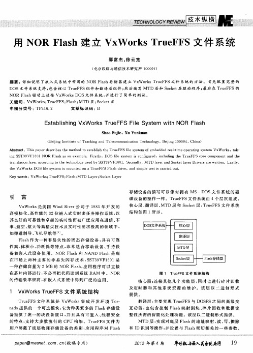
DS 系 }_ 心 0 件 统-_ 层I 文 . 1核
l 译 l l翻 层 I
Fah 为 一种 非 易 失 性 的 固 态 存 储 设 备 , 有 可 靠 ls 作 具 性 高 、 积 小 、 耗 低 等 特 点 , 常 适 合 移 动 设 备 、 持 设 体 功 非 手
核 心 层 : 接 其 他 几 个 功 能 层 , 时 也 进 行 碎 片 回 收 连 同 及 定 时 器 和 其 他 系 统 资 源 的 维 护 。该 层 以 二 进 制 形 式
基于NANDFlash的嵌入式文件系统μC/FS的实现
( 南 大学 集成 电路 学 院 。 苏 南 京 2 0 9 ) 东 江 10 6
摘要 : 绍 了基 于 NANDFah的 嵌入 式 文件 系统 的 实现 , 介 ls 其硬 件 平 台是 嵌 入 式 芯 片 S P 0 0与 NANDFah结 合 的 高性 能 嵌入 式 E 42 I s
3在 S P 0 0上实现嵌 入式 文件 系统  ̄ /S E 42 CF
M ci 公 司 的  ̄ /SJ 高度 可移 植 、 固化 的 嵌 入 i u rm CF L 2 是 可 式 F T文件 系统 。I /S的设 备驱 动 结 构非 常简 单 , 需 A  ̄ F C 只 要 读 写 扇 区的 底层 函数 。对 于 未 格 式化 的设 备 , 需 要 提术 原 理 C 8lF
T 5 5 2 东 芝公 司 出产 的 6 M 字 节(y ) A D Fah芯 片 。其 存 储 空 间分 为 4个  ̄(l e 4 9 块 (l k, C 8 1H ̄ I 是 4 BtN N l e s Pa ) 0 6个 Bo )每个 块 分 n共 c 为3 2页(ae, 页 为 5 8字 节 , 中 1 节 是 用来 形 成 Pg)每 2 其 6字 N N A D结 构 的 , 际存 储 数据 使 用 5 2 节 。擦 除 至 少是 实 1字 表 1 P B B结构 对 一 块操 作 , 写 可 以对 页 进行 操 作 。要 对 某 页 进 行 写操 读 作前 . 必须 先 进 行 擦 除 操 作 , 而一 次 除擦 的最 少 空 间是 一 个 块 , 果该 块 中其他 页 已经存 在 数 据 , 须 先备 份 起 来 , 如 必 然 后 在擦 完 该块 后 . 一 起 写 到指 定 区域 。 再
1引 言
嵌入式设备NAND Flash存储系统的设计与实现
比如E T 、 X 2 F T 2等文件系统, X 3 E T 、A 3 由于我 们在接下来 的块
设 备 层 中 实 现 了 闪存 翻 译 层 (T )所 以文 件 系 统 可 以采 用 任 F L, 何 通 用 的 文 件 系 统 , 不 需 要 采 用 特 殊 的针 对 N N l h 而 A DFa 的 s 文件 系 统 , 比如 J F 2等 ,块 设 备 驱 动 层 , 主 要 实 现 统 一 的 FS Lnx 设 备 驱 动 , 要 完 成 块 设 备 注册 、 义 块 设 备 操 作 、 i 块 u 主 定 请
Ab t a t T e eo o a es se i mb d e e ie t e sr c : od v lp a tr g tm e e d dd v c , h s y n NAND l s a d l s dlr e c p ct o a ed v c u i d F a ht t wi eyu e g - a a i s r g e i e s t d e . h a a yt is A e in o NAND ls o a es se f r mb d e e i e t d c d n s u c in n o si t r r p s d h a t u a d s f g F a hs r g y tm t o e e d dd v c s s n r u e ,a d i n t s dc n t e ep o o e .T e ri lr ii o tf o a u t a p c d sg x li e i rr hc l . T e s e il l c rv r F L d sg n eo t z t n o r e i ai ai n a e li ea l e i i e p an d h e ac ia l n s y h p c a o k d i e , T e in a d t p i a i f i ri t l t r d i d t i b h mi o d v n i z o a n . A t o f e l i gNAND ls tr g y t m e i ed i e si p o i e . F n l , t e e c l n fe t si u n t d me h do r ai n z F a h so a es se d v c rv r r v d d s i al y h x el t e e c lmi a e . i l
NAND Flash存储管理的jkffs嵌入式文件系统说明书

International Conference on Communication and Electronic Information Engineering (CEIE 2016)To establish file system in industrial storage managementHui-Zhong LiuInstitute of Applied Mathematics Hebei Academy of sciences, Shijiazhuang, 050081,ChinaE-mail:****************Aiming at the Nand flash which is widely used in industrial storage management, theembedded file system named “jkffs”is established. In “jkffs”, a direct addressingalgorithm is described; tnode-tree, variable-tnodelength are used to address most kinds ofnand flash; the method of chunk group is mentioned also. The dynamic wear-levelingalgorithm and static wear-leveling algorithm according to the different erasing times ofblock are presented in “jkffs” to realize the garbage-collection and wear-leveling.Keywords: Jkffs; Ttnode-tree; Variable-tnodelength; Tthreshold.1. IntroductionNAND Flash memory is widely used in the industrial storage management in which embedded system is the core. The log-structured file system designed according to the physical structure characteristics of NAND Flash can solve the embedded system of mass storage management issues.NAND Flash array can be divided into a series of blocks. Each block contains a number of pages, and the block is the smallest erasable unit. Erasing a block means defining all the bits as "1" (defining all bytes as “FFh”). Writing operation, through the programming, turns erased bits from "1" to "0". The unit of reading and writing is the page, the page contains data area and leisure area (OOB, out-of-band), and OOB area is used for software designer. Writing Page and erasing block are the basic operations of NAND Flash. Programming all bytes of blocks for OXFF can release space [1].2. Establishment of The File System2.1. The basic ideas of the file systemThe file system we establish is named “jkffs”. Additional information is stored in OOB area, which is designed to realize the management of NAND FLASH.All the components in the file system, including file, directory, links, devices etc., are entirely regarded as a file .Each file has a special head page store file to preserve the head of mode, length, file name, father object labeling and other information. The basic unit for writing in NAND Flash is the Page (Page) called chunk in the file system, which has different meanings. Page refers to the actual data storage areas on the NAND Flash Memory, while the chunk is the logical data storage areas allocated by the file system. Their sizes can be different.With 2048+64byte as a page of NAND Flash chips, for example, the file system use 8 Byte on OOB district to store the relative file system information [2], and design a erasing-times mark (Erase_num, 8 bits), to recover block and realize the wear-leveling. The directory structure of the file system must be built in the memory during the process of loading the system. Reading OOB contents is only needed to scan each Chunk and from the system marks in the OOB, it can be determined whether the Chunk is head or data. Then according to the contents of the file head chunk and the information such as object ID, chunk ID of data chunk, establish a corresponding object in the memory for each file. After all the Block has been scanned, it would establish the relationships of all objects, and form a kind of architecture in RAM. Thus, the file system would be loaded successfully [3].2.2. Addressing of the file systemEfficient addressing can be realized by creating a node tree. Structure definition: union jkffs_Tnode_union {union jkffs_Tnode_union *internal[8];}This is a pointer array of length 8. The node tree at the bottom, created according to this structure, becomes the leaf nodes and the middle is internal node. They have the same structure. When the nodes is the internal nodes, each element of the array will point to the next layer of child node; When the node is the leaf node, the array will be splitted into 16 long integer with N bits (Tnodelength), which is the storage location of the file contents in the flash (that is, chunkid).The Tnodelength of leaf nodes determines the maximum addressed space for the file system. For example, Tnodelength = 16, means it can represent 216 =65536 chunk.. As for a NAND flash with 2K chunk , the largest flash address space c is 128 M.It is very convenient to find the files through the node tree. Each tnode used by the internal node has 8 pointers, so three binary codes are needed to index it,therefore when the tree grows a layer high, three codes would be added into the ChunkID. In turn, each three nonzero ChunkID represents a layer of the internal nodes. Meanwhile, each Tnode used by leaf nodes has 16 pointers, so four binary codes are needed to index it.When tnode structure just started to be built, only the lowest level tnode would be established. And when the number of the Chunk was more than 16, an internal tnode would be established in the tree, and NO. 0 pointer would point to the Lowest Level Tnode. While more and more Chunk is read, new tnode will be added and the node tree is also more and more higher.2.3. Variable-Tnodelength in the node treeTnodelength of bottom node in the node tree determines the maximum space which can be addressed by file system . If The size of the chunk is 512 byte, 32 MB NAND Flash need 65536 chunks, and it needs 16 bit to index chunk. Similarly, 64MB nand flash needs at least 17 bit to index all the chunk and 128 MB NAND Flash needs18 bit. In order to facilitate processing, the tnodeSize must be the multiple of 32bit, tnodeSize = (tnodelength * 16) / 8, the unit is Byte. Tnodelength represents the length, because the Tnode of level 0 is 16 physical chunk index. From the foregoing, tnodelength is the size of physical chunk index, and the unit is bit. In order to make tnodeSize the multiple of 4 Byte, 64 M flash’s chunk index bits has to be 18 bit at least. Thus tnodelength = 18 can directly addressed 128 MThe way by increasing tnode-length can realize the management of the most large capacity of NAND Flash on the market at present, say, tnodelength = 20, the file system has the maximum space: 220 * 2 K = 2G for addressing. But such established node tree occupy too much RAM space in embedded system, which affects system performance, and it is not quite flexible for the protean design of embedded system.In system initialization process the information of NAND Flash is first read, the total number of pages can be obtained by multiplying blocks of Flash ( nblocks) by pages of each block, which means that file system need to manage these pages, and then figure out tnodelength of bottom node .specific algorithm is as follows:1) C alculated the total number of pages x = nChunksPerBlock * nBlocks2) w hen X > 1, shift X 1 to right ,bits= bits+13) r epeat , until x <= 14) i f X is odd number,X=X+15) endFlow chart as shown in Fig. 1Bits is bit length, and assign to tnodelength. This way can solve the problem that fixed tnodelength occupies too much RAM in the system, and can manageFig. 1 Tnode-length algorithm flow chartIn the actual system design, if bits is too large, Chunk array can be considered. Make one Chunk to match more pages, through which can reduce the tnodelength.Thus,the goal of managing NAND Flash memory can also be achieved. That is, through synthesizing certain chunk into a group with a same Id, may also increase the addressing chunk scope. At this time, the Pages of chunk are different. Supposing that a Chunk corresponds two pages andtwo continuous pages can becalled d_Chunk, including 4096bytes data, here d_Chunk [0], d_Chunk [1] correspond relevant page separately, as shown in Fig. 2:Fig. 2 Chunk array and Page relationship schemes3. Garbage- Collection and Wear-LevelingThe life of the flash memory is limited, it is determined by the maximum erasing time of the block .Therefore, wear-leveling algorithm should be design to distribute the erasing and writing operation evenly on each block and its impact on performance should be as low as possible. The process of erasing blocks and reuse it is called “garbage-collection”. Considering the using frequency of data with garbage-collection and wear-leveling, we designed two algorithms: dynamic and static wear-leveling algorithm.3.1. Dynamic wear-leveling algorithmThe working range of Dynamic wear-leveling algorithm is the updated frequently data space and unused space, it will be realized in the writing of data.Fig. 3 Garbage-collection Flow chartThe algorithm supplies a good way to manage the dynamic data in flash memory. It can guarantee a fixed number of free blocks, as well as can solve data writing delay and accumulation. Two values were used in the blockrecovery algorithm above, they are Min and TH1. Min is the number of recovered dirty block each time when the idle block list is empty. Next, TH1will be explained.In this algorithm, garbage-collection will happen when free block list is empty, while the recovery of dirty block may need to copy the effective data of dirty block first, so the erasing should be done by descending order of useless data page when recovering block, here TH1 means the lower limit of dirty block though “Aggressive Mode”, the recovery can be operated from the beginning of the list of dirty block when the value is more than that.The Min must meet the conditions for Min ≥ TH1.If Min is too large, the number of free blocks will increase, accordingly, the available memory space will reduce; If Min is too small, it cannot solve the problem of data accumulation completely. In the file system, Min is 1/10 of the total block, namely Min = nBlocks / 10, TH1 = Min / 2.3.2. The realization of static wear-levelingIn the practical application of the embedded system data storage have such characteristics: most files are small files, but large files take up most of the storage space; the blocks of small files are updated much frequently. Thus the following situation will appear: the erasing blocks of small files have more erasing times than that of big files, which leads erasing times of small files’erasing blocks will reach the upper limit of erasing times faster and the life of the whole flash memory will be used up.In order to deal with this kind of static read-only data, we designed static wear-leveling algorithm. When the garbage-collection was triggered, read the EraseNum from OOB of the erase block in the clean blocks list, which marked the erasing times, then find out biggest and smallest erasing times. Then do subtraction between them, if the value is bigger than threshold, it can be concluded that erase with minimum number of erasing stored static data, and it needed to be moved. And because the static data are usually bigger and take up more erase blocks, the number of blocks with the minimum time of erasing is more than 1. Therefore, in order to better achieve erase equilibrium, it is necessary to scan the clean block list again after moving operation, and find out the block with maximum erasing times. Specific algorithm is divided into the following steps:1)S can clean block list, and find out the blocks with the biggest and smallest erasing times, then record the number EraseMax and EraseMin respectively, and name the blocks A and B respectively.2) I f “EraseMax - EraseMin≥TH2”, erase block B store the static data, it must be done with moving operation.3) s elect one block from the free block list, copy the data of A to it; Then erase A, and then copy the data of B to A; And then put B to the dirty block list for the storage of data updated frequently.4) R epeat above three steps, until “EraseMax - EraseMin≥TH2” is false, That is, all the static data have been moved.The value of TH2 is very important in the algorithm. If the threshold is too large, the number of static file storage blocks needed to be released will be greater than that of free blocks, and effective data cannot be all received. Conversely, if threshold is too small, blocks for static data file storage cannot be released promptly, and frequent data moving will affect the performance of the system. Usually it is better to set the value of TH2 between 200 to 500. In this file system TH2 = 250.4. ConclusionAt present the most reasonable management of NAND flash memory of the file system mostly uses the log-structured design ideas, such as JFFS, yaffs, etc. The file system “jkffs ” is developed and completed .Practice has proved that “jkffs ” could flexibly manage many NAND Flash with various size at present. References1. Samsung Corp. Flash Memory K9K4G08U0M DataSheet[S], Nov. 2015.2. SUN Feng and ZHANG Fu-xin, “Research an Improvement Of YAFFSFile System”, Computer Engineering, vol. 34, pp. 258-261 March 2014.(In Chinese).3. Wookey. YAFFS Direct User Guide. 2013-07-26. http :// /.。
- 1、下载文档前请自行甄别文档内容的完整性,平台不提供额外的编辑、内容补充、找答案等附加服务。
- 2、"仅部分预览"的文档,不可在线预览部分如存在完整性等问题,可反馈申请退款(可完整预览的文档不适用该条件!)。
- 3、如文档侵犯您的权益,请联系客服反馈,我们会尽快为您处理(人工客服工作时间:9:00-18:30)。
数据操作。一些基本操作实现如下: () " 设备识别# VDDG (679^169A1NWA 读取 ;&68C 的设备标志号 A1NWA, 根据 A1NWA 确定 ;&68C 的型 号, 从而获取存储器的相关参数如: 容量、 电压、 总块数、 每块页 数、 每页主数据区大小和空闲区的大小。 ( SGD(O J&%5‘3992) " 擦除# VDDG (679V&%5‘Z2681
#*)+,! "!# +-./*-*!0"0+1! 1$ $$) $12 !"!# $/")3
:C17 =467C/6# G/% H/1I4
( !"#$%&’"(& )* +)’#,&"% -./"(.", 0$1& +2/($ 3)%’$4 5(/6"%1/&7, -2$(82$/ 9:::;9 , +2/($)
! ! "" ! ! !
擦除块地址为 &’()*+,,- 的块。操作过程如下:
计算机应用与软件
#$$% 年
789:+,,- 为逻辑扇区地址, L-)4EF 为要写入的数据。操作 过程如下: 0 )对 789:+,,- 计算 得 到 逻 辑 块 地 址 + 和 页 偏 移 地 址 8 ( 789:+,,- U +!S# V 8) ; # )若 &’()*=8&’: [ +]U ?>66, 进行空块分配获取块 W, 在空 块上记录 G?>DP 状态和逻辑块地址, 写入 L-)4EF 数据到 W 第 8 页, 更新 &’()*=8&’: [ +]U W; S )若 &’()*=8&’: [ +]U 4, 读取块 4 第 8 页状态。 NCPP 则 直接写入数据; G?>DP 需擦除才能改写。重新分配逻辑块 +, 修 改块 4 和页 8 的状态为 5>H>DP。获取空块 W, 记录 G?>DP 状 态和逻辑块地址, 写入 L-)4EF 数据到 W 第 8 页, 更新 &’()*=8&’: [ +]U W。 读扇区: D:)=(-C:8, ( >65?@, 789:+,,-, >3B+C!,L=4EF) 789:+,,- 为逻辑扇区地址, ,L=4EF 存放读出的数据。读扇 区操作只需对 789:+,,- 计算得到逻辑块地址 + 和页偏移地址 8 ( 789:+,,- U +!S# V 8) , 直接读出块 4 第 8 页数据即可。 " 碎片回收 X(<, ,<L*3’:8I () 搬移状态为 5>H>DP 的块, 擦除状态为 G?R+6G1 的块。一 张无效 T 正常使用块对应表记录状态为 5>H>DP 的块的物理 块地址以及其对应的逻辑块地址。 碎片回收在空闲时或表满时进行。根据对应表中记录的逻 辑块地址 Q, 在逻辑 T 物理块地址映射表中读出 Q 重新分配到 的新的物理块地址 Y, 依次把 W 中不为空的页读出, 分别写入 Y 中。最后擦除 W, 擦除次数加 0 。 特殊整理: R(<, LA:)3’:8I () 为了解决静态数据的问题而定期进行的特殊整理。比较各 块的擦除次数, 对于使用频率明显低于平均水平的块, 搬动这些 块的数据, 让这些使用很少的块供另外的数据使用, 从而更好地 均衡整体使用寿命。注意这种整理不能太频繁, 否则反而会降 低磨损控制的效果。
@8 $$) 的功能结构
根据功能模块划分, BB: ( B&68C B4&1 :I801-) 可分为三层, 如 图 @ 所示。 最底层是硬件操作接口, 它和硬件 直接相关, 封装 (3(A B&68C 具体的物 理操作; 往上是文件传输层 ( BFG ) , 主 要功能是针对 (3(A B&68C 的特性, 封 装一些特殊的复杂的管理控制功能, 使 得上层操作 B&68C 就 和 操 作 普 通 磁 盘
收稿日期: !**> ? *! ? @" 。沈建华, 副教授, 主研领域: 嵌入式实时 系统。
层提供标准的文件操作接口。
A8 结构设计与应用
AB ?8 结构设计
整个系统结构设计如图 ! 所示。硬件设计采用 ,HO(3G ,Q*+@B*!* 微处理器和 :3R:S(O TUB!Q*QS*V。 TUB!Q*QS*V
AB @8 硬件操作接。具体 硬件连接上, 命令、 地址和数据端口分别映射到某一片外地址空 间, 对端口操作就直接对片外某存储单元操作一样。 分别定义端口如下:
]91;471 A3F3 ]91;471 ,RA ]91;471 3AA^ XD^F *Y1*** XD^F *Y1*@* XD^F *Y1**Q
图 !# 系统结构
?8 引8 言
新世纪嵌入式系统市场发展迅速, 主要表现在通信、 消费电 子产品和多媒体应用。在这些嵌入式计算机系统中, 存储设备 的性能是决定整体系统性能的核心环节之一。 B&68C 存储器具 有容量大、 速度快、 成本低等很多优点, 因此在嵌入式系统中的 应用也越来越多。由于物理特性的不同, 基于 BG3:P 的文件系 统也不同于普通磁盘上的文件系统。不同应用系统中 BB: 的 设计实现也有所不同。本文的方案特点是具有较好的磨损控制 功能和与 E479%<8 文件系统完全兼容。
"4’56&758 8 (3(A B&68C 48 6 5C16. J/0 ;471 -1-%2I 679 BB: ( B&68C B4&1 :I801-) 48 67 1;;454170 <6I 0% C679&1 0C1 C/K1 6-%/708 %; 9606 47 0%96IL8 1-J19919 8I801-) FC1 8.1546& ;4&1 8I801- ;%2 (3(A B&68C 48 4702%9/519 47 0C48 .6.12, 6&8% 6 9184K7 679 67 4-.&1-170604%7 48 ./0 ;%2M <629) 9:;<=6>’8 8 BB:# (3(A B&68C# B3F# E162M&1N1&47K# O62J6K1 5%&&1504%7 是 @"R ! QJ40 的 (3(A BG3:P, ,PWX WA 为 *YZ,M*Y[\ , 存储单位 有字 节、 页 和 块。每 页 +!Q 个 字 和 节, 由 ! 个 !+" 字节主数据区, 一个 @" 字节空闲区组成; \! 页为 一块, 共 @*!> 块。 在软件结构上分别实现 (3(A B&68C 物理接口、 BFG 和 B3F 从而实现一个完整的 BB:。
第 !! 卷第 " 期# # # !**+ 年 " 月# #
计算机应用与软件 ,%-./012 3..&45604%78 679 :%;0<621
$%&’ !! , (%) " =/7) !**+
基于 !"!# $%&’( 的 $$) 设计与实现
沈建华# 罗悦怿
( 华东师范大学计算机科学技术系# 上海 !***"! )
图 @# BB: 体系结构 一样; 最上层是文件管理层, 功能类似 于普通磁盘上的通用文件系统, 封装一些文件管理等功能, 向上
(3(A B&68C 的命令有 ^169,C4.WA, ^169, X2%K26- 和 Z2681 等。往 ,RA XD^F 写 命 令 代 码 输 出 一 个 命 令, 往 3AA^ XD^F 读 _ 写数据完成读写 XD^F 写入地址输出地址, 从 A3F3
摘# 要# # (3(A B&68C 以其大容量低价格等优势迅速成为嵌入式系统存储的新宠, 因此研究其上的文件系统也日益重要。本文先 分析了 (3(A B&68C 上 BB: 的功能结构, 然后给出了一个在无 D: 支持的嵌入式系统中, 可与 E479%<8 文件系统完全兼容的 BB: 的 设计和实现方案。 关键词# # BB:# (3(A B&68C# B3F# 磨损控制# 碎片回收