21ic--基于AM335x的工业自动化应用
03 AM335x处理器
• EMIF0 SDRAM
– 0x8000_0000 0xBFFF_FFFF, 1GB 8-/16-bit External Memory, (ex/e/w)
北京交通大学
国家电工电子教学基地
Main processor
ARM Cortex-A8 MPU子系统
• MPU 子系统处理 ARM A8核心 , L3 互联和中断控制 器 (INTC)之间的 数据交换. • MPU把A8处理器 和其他附加逻辑 集成在一起,实 现协议转换、仿 真、中断处理和 调试增强功能。
L3 Slow clock domain
目标模块 : 只能响应 r/w请求
To L4 interconnect
北京交通大学国家电工电子教学基地 Main processor
L4 互联结构*
北京交通大学
国家电工电子教学基地
Main processor
片上模块 (驱动开发相关)
• cache : 高速缓存 • mDDR: 移动双倍速率同步动态随机存储器 • PRU-ICSS: 可编程实时单元和工业用通信子系统
• AXI2OCP桥
– 支持OCP 2.2.
– 在两个端口实现单次请求多个数据协议。 – 多个目标,包括三个 OCP ports (128-bit, 64-bit and 32-bit).
• 中断控制器
– 最多支持128个中断请求
• 仿真/调试
– 与CoreSight结构兼容
• 时钟产生
– 通过PRCM(电源、复位、时钟微控制器)
北京交通大学
国家电工电子教学基地
Main processor
存储器子系统: GPMC
• GPMC 为器件提供访问NAND Flash, NOR Flash和其他异步/同步接 口外设 的手段.
CES-AM335X 产品手册说明书

深圳市海天雄电子有限公司Shenzhen Haitianxiong Electronic Co., Ltd. CES-AM335X产品手册TI系列开发平台Rev. V1.0Date:2016-08-03平台简介CES-AM335X开发平台是海天雄研发的一款工业级开发平台,基于TI公司Sitara系列的ARM处理器AM335X,在设计上采用高集成度的系统模块形式的核心板,核心板上集成了容量512MB的DDR3颗粒,容量1GB的SLC NandFlash 和电源管理芯片。
CES-AM335X开发平台由核心板、底板、显示驱动板、开发辅助工具组成,核心板采用AM3354,是产品定位最清晰的一个工业控制MCU,最高运行频率可达800MHz,集成了基于ARM Cortex-A8的微处理器单元、两路MAC控制器和POWERVR SGXTM图形加速器,在图像、图形处理、外设方面进行了增强,保证系统在低功耗运行的同时拥有高性能,核心板可直接用于目标产品,从而节省开发时间和开发成本;底板由各功能单元和扩展模块组成,功能单元包括常用的UART 串行数据口、USB主/从设备通用串行数据口、以太网接口、I2C通信接口、CAN通信接口、RS485通信接口、MMC/SDIO 接口、McASP接口、ADC接口、AUIAO、LVDS和RGB双路显示控制接口、GPIO输入输出功能及其他功能。
CES-AM335X开发平台可选7英寸电阻触摸液晶显示屏和10.1英寸电容触摸液晶显示屏,提供配套的开发工具包和软件程序包。
丰富的资源、优化的软硬件,完全满足大多数产品的应用,适用于工业控制、医疗电子、节能环保、智能交通、能源节能、电力系统、通讯系统、数控行业、汽车电子、工业触摸屏控制系统、机器人视觉、媒体处理无线应用、数字家电、车载设备、通信设备、网络终端等环境恶劣场合。
平台特点◆TI Cortex-A8 AM3354处理器;◆搭载512MB DDR3内存和1GB SLC NandFlash;◆支持7英寸RGB 24位电阻触摸显示屏(800*480)及10.1英寸LVDS(1024*600)显示屏;◆支持双路千兆以太网接口,包含RS485、CAN总线、USB等,满足工业应用;◆支持Linux3.2、Android4.2操作系统;功能接口核心板硬件参数软件参数——Linux 3.2软件参数——Android 4.2USB 摄像头驱动 支持USB 摄像头的预览和拍照功能 CAN 驱动 支持CAN 通讯 RS485驱动 支持RS485通讯 SPI 驱动支持SPI 通讯产品配置清单开发平台(扩展板+核心板)用户光盘串口线触摸笔网线10.1英寸电容触摸显示屏USB 线7英寸RGB 电阻显示屏(选配)电源适配器SD 卡(选配)服务支持技术支持联系方式:电话:*************86325376邮箱:************************技术支持服务时间:周一至周五:9:00~12:00,13:30~18:00免责声明本手册信息仅供用户参考使用,对于所作修改,恕不另行通知。
基于AM335X的智能采集器模块设计

硬件与结%Hardware and Architecture基于AM335X的智能采集器模块设计+李要中##刘钧2,马尚昌#,3(1.成都信息工程大学电子工程学院,四川成都610225;2.华云升达(北京)气象科技有限责任公司,北京102299;3.中国气象局大气探测重点开放实验室,四川成都610225)摘要:为了适应气象现代化、智能化的发展趋势,解决系统结构复杂、布线繁琐等问题,提出了一种基于A M335X的智能采集 器模块设计方法,实现对传感器信号的高精度采集与处理。
系统依托U b u n t u嵌入式软件开发平台;硬件部分利用模块化结构 设计,将相似的部分划在一起,尽量避免模块间的相互衔接,增强了体系的可靠性,同时提升了设计的层次化标准。
软件部分基 于S e c u r e C R T测试环境,搭建函数动态链接库,采用多线程通信结构,使得软件结构简单,易于实现。
测试结果表明:该模块能 有效地实现对数据的采集处理,符合应用要求。
关键词!A M335X;智能采集器;嵌入式软件;数据处理中图分类号:T P31 文献标识码:A D O I: 10. 19358/j.is s n.1674-7720.2017. 15.009引用格式:李要中,刘钧,马尚昌.基于A M335X的智能采集器模块设计[J].微型机与应用,2017,36(15):32-34.Design of intelligent collector module based on AM335XL i Y a oz l io n g1,L iiu J u n2,M a S h a n g c h a n g1,3(1. C olleg e o f E le c tr ic a l E n g in e e rin g,C he n g du U n iv e rs ity o f In fo rm a tio n T e c h n o lo g y,C he n g du610225,C h in a;2. H u a Y u n Sheng D a (B e ijin g)M e te o ro lo g ic a l S cien ce a nd T e c h n o lo g y Co. ,L t d,B e ijin g102299,C h in a;3. K e y L a b o ra to ry o f A tm o s p h e ric S o u n d in g,C M A,C he n g du610225,C h in a)A b s tT c lC t:In o rd e r to a d a p t to th e m e te o ro lo g ic a l m o d e rn iz a tio n,in te llig e n t d e v e lo p m e n t tr e n d,to so lve th e c o m p le x system s tr u c tu r e,w irin g cum bersom e and o th e r is s u e s,a design m ethod o f in te llig e n t a c q u is itio n m o du le based on A M335X is p ro p o s e d,w h ic h can re alize the h ig h q u a litya c q u is itio n and s ig n a l p roce ssin g o f t!ie sensor. T h e system re lie s on Ub u n tu em bedded softw are d e ve lo p m e n t p la tfo rm. T he hard w a re p a rt uses them o d u la r s tru c tu re d e s ig n,it d iv id e s the s im ila r p arts to g e th e r,as fa r as p ossib le to a void the in te ra c tio n b etw een m o d u o f the s y s te m,and enhance the design o f the h ie ra rc h y s ta n d ard. T he softw are p a rt is based on S e cu re C R T te st e n v iro n m e n t to set up the fu n c tio no f d y n a m ic lin k lib ra ry. B y u sin g the m u lti th re a d c o m m u n ic a tio n s tru c tu re,m a k in g the softw are s tru c tu re is s im p le and easy to im p le m e n t. T he test re su lts s h o w th a t the m o du le can e ffe c tiv e ly achie ve the data a c q u is itio n and p ro c e s s in g,in lin e w ith the a p p lic a tio nK e y w o r d s:A M335X;in te llig e n t c o lle c to r;e m be d d ed softw are ;d ata p ro ce ssin g〇引言智能采集器解决了对传感器信号接人结构复杂、布线 繁琐的问题,具有智能化程度高、通用化、系统资源丰富、处理能力强、扩展方便等特点。
TIAM335x系列处理器6LoWPAN网络参考设计TIDA010032

TI公司的AM335x系列微处理器是基于ARM Cortex-A8处理器,工作频率高达1GHz,具有增强图像,图形处理,外设和工业接口选择如EtherCAT和PROFIBUS,支持高级操作系统(HLOS).器件还具有NEON™ SIMD协处理器,32KB L1指令和32KB数据缓存,256KB L2高速缓存,176KB引导ROM和64KB专用RAM,主要用在数据集中器和无线通信.本文介绍了AM335x处理器主要特性,功能框图以及支持以太网,6LoWPAN RF网络和更多的通用数据集中器参考设计TIDA-010032主要指标,网络指标,框图,系统架构图,电路图,材料清单和PCB设计图.The AM335x microprocessors, based on the ARM Cortex-A8 processor, are enhanced with image,graphics processing, peripherals and industrialinterface options such as EtherCAT and PROFIBUS. Thedevices supporthigh-level operating systems (HLOS). Processor SDK Linux® and TI-RTOS are availablefree of charge from TI.The AM335x microprocessor contains the subsystems shown in theFunctional Block Diagram and a briefdescription of each follows: The contains the subsystems shown in the Functional Block Diagramand a brief description of eachfollows:The microprocessor unit (MPU) subsystem is based on the ARM Cortex-A8 processor and the PowerVRSGX™ Graphics Accelerator subsystemprovides 3D graphics acceleration to support display and gamingeffects.The PRU-ICSS is separate from the ARM core, allowing independentoperation and clocking for greaterefficiency and flexibility.The PRU-ICSS enables additional peripheral interfaces and real-time protocolssuch as EtherCAT, PROFINET, EtherNet/IP, PROFIBUS, Ethernet Powerlink, Sercos, and others.Additionally, the programmable nature of the PRU-ICSS, along with its access to pins, events and allsystem-on-chip (SoC) resources, providesflexibility in implementing fast, real-time responses, specializeddatahandling operations, custom peripheral interfaces, and in offloading tasks from the other processorcores of SoC.AM335x处理器主要特性:• Up to 1-GHz Sitara™ ARM® Cortex®-A8 32 BitRISC Processor– NEON™ SIMD Coprocessor– 32KB of L1 Instruction and 32KB of Data CacheWith Single-ErrorDetection (Parity)– 256KB of L2 Cache With Error Correcting Code(ECC)– 176KB of On-Chip Boot ROM– 64KB of Dedicated RAM– Emulation and Debug - JTAG– Interrupt Controller (up to 128 InterruptRequests)• On-Chip Memory (Shared L3 RAM)– 64KB of General-Purpose On-Chip MemoryController (OCMC) RAMTI AM335x系列处理器6LoWPAN网络参考设计TIDA-010032– Accessible to All Masters– Supports Retention for Fast Wakeup• External Memory Interfaces (EMIF)– mDDR(LPDDR), DDR2, DDR3, DDR3LController:– mDDR: 200-MHz Clock (400-MHz Data Rate)– DDR2: 266-MHz Clock (532-MHz Data Rate)– DDR3: 400-MHz Clock (800-MHz Data Rate)– DDR3L: 400-MHz Clock (800-MHz DataRate)– 16-Bit Data Bus– 1GB of Total Addressable Space– Supports One x16 or Two x8 Memory DeviceConfigurations– General-Purpose Memory Controller (GPMC)– Flexible 8-Bit and 16-Bit AsynchronousMemory Interface With up toSeven Chip Selects (NAND, NOR, Muxed-NOR, SRAM)– Uses BCH Code to Support 4-, 8-, or 16-BitECC– Uses Hamming Code to Support 1-Bit ECC– Error Locator Module (ELM)– Used in Conjunction With the GPMC toLocate Addresses of Data Errors fromSyndrome Polynomials Generated Using aBCH Algorithm– Supports 4-, 8-, and 16-Bit per 512-ByteBlock Error Location Based on BCHAlgorithms • Programmable Real-Time Unit Subsystem andIndustrial Communication Subsystem (PRU-ICSS)– Supports Protocols such as EtherCAT®,PROFIBUS, PROFINET,EtherNet/IP™, and More– Two Programmable Real-Time Units (PRUs)– 32-Bit Load/Store RISC Processor Capableof Running at 200 MHz– 8KB of Instruction RAM With Single-ErrorDetection (Parity)– 8KB of Data RAM With Single-Error Detection(Parity)– Single-Cycle 32-Bit Multiplier With 64-BitAccumulator– Enhanced GPIO Module Provides Shift-In/Out Support and Parallel Latch on External Signal– 12KB of Shared RAM With Single-ErrorDetection (Parity)– Three 120-Byte Register Banks Accessible byEach PRU– Interrupt Controller (INTC) for Handling SystemInput Events– Local Interconnect Bus for Connecting Internaland External Masters to the Resources Insidethe PRU-ICSS– Peripherals Inside the PRU-ICSS:– One UART Port With Flow Control Pins,Supports up to 12 Mbps– One Enhanced Capture (eCAP) Module– Two MII Ethernet Ports that Support IndustrialEthernet, such as EtherCAT – One MDIO Port• Power, Reset, and Clock Management (PRCM)Module– Controls the Entry and Exit of Stand-By andDeep-Sleep Modes– Responsible for Sleep Sequencing, PowerDomain Switch-Off Sequencing, Wake-Up Sequencing, and Power Domain Switch-OnSequencing– Clocks– Integrated 15- to 35-MHz High-frequencyOscillator Used to Generate a Reference Clock for Various System and PeripheralClocks– Supports Individual Clock Enable and DisableControl for Subsystems and Peripherals toFacilitate Reduced Power Consumption– Five ADPLLs to Generate System Clocks(MPU Subsystem, DDR Interface, USB and Peripherals [MMC and SD, UART, SPI, I2C],L3, L4, Ethernet, GFX [SGX530], LCD Pixel Clock)– Power– Two Nonswitchable Power Domains (Real-Time Clock [RTC], Wake-UpLogic[WAKEUP])– Three Switchable Power Domains (MPUSubsystem [MPU], SGX530 [GFX], Peripherals and Infrastructure [PER])– Implements SmartReflex™ Class 2B for CoreVoltage Scaling Based On Die Temperature,Process Variation, and Performance(Adaptive Voltage Scaling [AVS])– Dynamic Voltage Frequency Scaling (DVFS)• Real-Time Clock (RTC)– Real-Time Date (Day-Month-Year-Day of Week)and Time (Hours-Minutes-Seconds) Information– Internal 32.768-kHz Oscillator, RTC Logic and1.1-V Internal LDO– Independent Power-on-Reset(RTC_PWRONRSTn) Input– Dedicated Input Pin (EXT_WAKEUP) forExternal Wake Events– Programmable Alarm Can be Used to GenerateInternal Interrupts to the PRCM (for Wakeup) orCortex-A8 (for Event Notification)– Programmable Alarm Can be Used WithExternal Output(PMIC_POWER_EN) to Enablethe Power Management IC to Restore Non-RTCPower Domains• Peripherals– Up to Two USB 2.0 High-Speed DRD (Dual-Role Device) Ports WithIntegrated PHY– Up to Two Industrial Gigabit Ethernet MACs (10,100, 1000 Mbps)– Integrated Switch– Each MAC Supports MII, RMII, RGMII, andMDIO Interfaces– Ethernet MACs and Switch Can OperateIndependent of Other Functions – IEEE 1588v2 Precision Time Protocol (PTP)– Up to Two Controller-Area Network (CAN) Ports– Supports CAN Version 2 Parts A and B– Up to Two Multichannel Audio Serial Ports(McASPs)– Transmit and Receive Clocks up to 50 MHz– Up to Four Serial Data Pins per McASP PortWith Independent TX and RX Clocks– Supports Time Division Multiplexing (TDM),Inter-IC Sound (I2S), andSimilar Formats– Supports Digital Audio Interface Transmission(SPDIF, IEC60958-1, and AES-3 Formats)– FIFO Buffers for Transmit and Receive (256Bytes)– Up to Six UARTs– All UARTs Support IrDA and CIR Modes– All UARTs Support RTS and CTS FlowControl– UART1 Supports Full Modem Control– Up to Two Master and Slave McSPI SerialInterfaces– Up to Two Chip Selects– Up to 48 MHz– Up to Three MMC, SD, SDIO Ports– 1-, 4- and 8-Bit MMC, SD, SDIO Modes– MMCSD0 has Dedicated Power Rail for 1.8 Vor 3.3-V Operation– Up to 48-MHz Data Transfer Rate– Supports Card Detect and Write Protect– Complies With MMC4.3, SD, SDIO 2.0Specifications– Up to Three I2C Master and Slave Interfaces– Standard Mode (up to 100 kHz)– Fast Mode (up to 400 kHz)– Up to Four Banks of General-Purpose I/O(GPIO) Pins– 32 GPIO Pins per Bank (Multiplexed WithOther Functional Pins)– GPIO Pins Can be Used as Interrupt Inputs(up to Two Interrupt Inputs per Bank)– Up to Three External DMA Event Inputs that canAlso be Used as Interrupt Inputs– Eight 32-Bit General-Purpose Timers– DMTIMER1 is a 1-ms Timer Used forOperating System (OS) Ticks– DMTIMER4–DMTIMER7 are Pinned Out– One Watchdog Timer– SGX530 3D Graphics Engine– Tile-Based Architecture Delivering up to 20Million Polygons per Second – Universal Scalable Shader Engine (USSE) isa Multithreaded EngineIncorporating Pixel and Vertex Shader Functionality– Advanced Shader Feature Set in Excess ofMicrosoft VS3.0, PS3.0, andOGL2.0– Industry Standard API Support of Direct3DMobile, OGL-ES 1.1 and 2.0,and OpenMax– Fine-Grained Task Switching, LoadBalancing, and Power Management– Advanced Geometry DMA-Driven Operationfor Minimum CPU Interaction – Programmable High-Quality Image Anti-Aliasing– Fully Virtualized Memory Addressing for OSOperation in a UnifiedMemory Architecture– LCD Controller– Up to 24-Bit Data Output; 8 Bits per Pixel(RGB)– Resolution up to 2048 × 2048 (WithMaximum 126-MHz Pixel Clock)– Integrated LCD Interface Display Driver(LIDD) Controller– Integrated Raster Controller– Integrated DMA Engine to Pull Data from theExternal Frame BufferWithout Burdening theProcessor via Interrupts or a Firmware Timer– 512-Word Deep Internal FIFO– Supported Display Types:– Character Displays - Uses LIDD Controllerto Program these Displays– Passive Matrix LCD Displays - Uses LCDRaster Display Controller toProvideTiming and Data for Constant GraphicsRefresh to a Passive Display – Active Matrix LCD Displays – UsesExternal Frame Buffer Space andtheInternal DMA Engine to Drive StreamingData to the Panel– 12-Bit Successive Approximation Register(SAR) ADC– 200K Samples per Second– Input can be Selected from any of the EightAnalog Inputs MultiplexedThrough an 8:1 Analog Switch– Can be Configured to Operate as a 4-Wire, 5-Wire, or 8-Wire ResistiveTouch Screen Controller (TSC) Interface– Up to Three 32-Bit eCAP Modules – Configurable as Three Capture Inputs orThree Auxiliary PWM Outputs– Up to Three Enhanced High-Resolution PWMModules (eHRPWMs)– Dedicated 16-Bit Time-Base Counter WithTime and Frequency Controls – Configurable as Six Single-Ended, Six Dual-Edge Symmetric, or ThreeDual-Edge Asymmetric Outputs– Up to Three 32-Bit Enhanced QuadratureEncoder Pulse (eQEP) Modules • Device Identification– Contains Electrical Fuse Farm (FuseFarm) ofWhich Some Bits are Factory Programmable– Production ID– Device Part Number (Unique JTAG ID)– Device Revision (Readable by Host ARM)• Debug Interface Support– JTAG and cJTAG for ARM (Cortex-A8 andPRCM), PRU-ICSS Debug– Supports Device Boundary Scan– Supports IEEE 1500• DMA– On-Chip Enhanced DMA Controller (EDMA) hasThree Third-Party Transfer Controllers (TPTCs)and One Third-Party Channel Controller(TPCC), Which Supports up to 64 Programmable Logical Channels and EightQDMAChannels. EDMA is Used for:– Transfers to and from On-Chip Memories– Transfers to and from External Storage(EMIF, GPMC, Slave Peripherals)• Inter-Processor Communication (IPC)– Integrates Hardware-Based Mailbox for IPC andSpinlock for Process Synchronization BetweenCortex-A8, PRCM, and PRU-ICSS – Mailbox Registers that Generate Interrupts – Four Initiators (Cortex-A8, PRCM, PRU0,PRU1)– Spinlock has 128 Software-Assigned LockRegisters • Security– Crypto Hardware Accelerators (AES, SHA,RNG)– Secure Boot • Boot Modes– Boot Mode is Selected Through BootConfiguration Pins Latched on the Rising Edge of the PWRONRSTn Reset Input Pin • Packages:– 298-Pin S-PBGA-N298 Via Channel Package(ZCE Suffix), 0.65-mm Ball Pitch– 324-Pin S-PBGA-N324 Package(ZCZ Suffix), 0.80-mm Ball PitchAM335x处理器应用:• Gaming Peripherals• Home and Industrial Automation • Consumer Medical Appliances • Printers • Smart Toll Systems• Connected Vending Machines • Weighing Scales • Educational Consoles • Advanced Toys图1:AM335x处理器功能框图支持以太网,6LoWPAN RF 网络和更多的通用数据集中器参考设计TIDA-010032IPv6-based grid communications are becoming the standard choice in industrial markets and applications like smart meters and grid automation. The universal data concentrator design provides a complete IPv6-based network solution integrated with Ethernet backbone communication, 6LoWPAN RF mesh networking, RS-485 and more. The 6LoWPAN mesh networking addresses key concerns such as standard-basedinteroperability, reliability, security and long-distance connectivity. This design allows controlling and monitoring end devices remotely with a webserver accessible via Ethernet backbone communication. It also provides 3.3V and 5V voltage rails and various peripheral interfaces to extend to additional connectivity such as broadband power-line communication (PLC), cellular and Wi-Fi®.参考设计TIDA-010032主要特性:Implements universal data concentrator supporting Ethernet, 6LoWPAN mesh and RS-485 connectivity devicesAllows Internet of Things (IoT) services with web server and Ethernet backbone connectivityImplements 6LoWPAN RF mesh network protocols of 6LoWPAN, RPL, IPv6/ICMPv6 and UDPIntegrates with TI 15.4-Stack that supports frequency hopping (FH) and data encryption Fully compatible with the TIDA-010003 and TIDA-010024 end-node reference designs to provide a complete network solution Capable of extending to other connectivity devices such as broadband PLC, cellular and Wi-Fi参考设计TIDA-010032应用:Data concentrators Wireless communications图2:参考设计TIDA-010032外形图。
21ic-基于AM335x的 EtherCAT&CAN功能演示

第1题:AM335x对EtherCAT主站通信的支持可由哪个模块实现??APMUBPRUCGPUDEtherCAT正确答案:B,D所选答案:A第2题:目前TI官方提供的EVM板中,适合进行EtherCAT从站通信测试的有以下哪些?AGP EVMBStarterKitCICE EVMDBeagleBone正确答案:C所选答案:A第3题:对于操作系统的支持,AM335x现在可以提供的有哪些方案??AWINCEBLINUXCANDROIDDSYS/BIOS正确答案:A,B,C,D所选答案:A第4题:以下哪个型号是可以实现对EtherCAT从站通信支持的?AAM3359BAM3358CAM3357DAM3356正确答案:A,C所选答案:A第5题:AM335X在HMI应用中使用的3D图形显示效果是由以下哪个模块来加速实现的?AMPUBPRUCGPUDPMU正确答案:C所选答案:A第1题:目前TI官方提供的EVM板中,适合进行EtherCAT从站通信测试的有以下哪些?A GP EVMB StarterKitC ICE EVMD BeagleBone正确答案:C所选答案:A第2题:AM335x对EtherCAT主站通信的支持可由哪个模块实现??A PMUB PRUC GPUD EtherCAT正确答案:B,D所选答案:A第3题:在GPEVM上CAN通信通过DB9接口接出,通信介质的选择是?A2、3、5线直连的串口线B2、3线交叉,5线直连的串口线C2、3、7线直连的串口线D2、3线交叉,7线直连的串口线正确答案:C所选答案:A第4题:在GPEVM板上演示CAN通信的运用中,PROFILE的选择应设定为模式几?A Mode 0B Mode 1C Mode 2D Mode 3正确答案:B所选答案:A第5题:AM335X在HMI应用中使用的3D图形显示效果是由以下哪个模块来加速实现的?A MPUB PRUC GPUD PMU正确答案:C所选答案:A第1题:目前TI官方提供的EVM板中,适合进行EtherCAT从站通信测试的有以下哪些?A GP EVMB StarterKitC ICE EVMD BeagleBone正确答案:C所选答案:A第2题:对于操作系统的支持,AM335x现在可以提供的有哪些方案??A WINCEB LINUXC ANDROIDD SYS/BIOS正确答案:A,B,C,D所选答案:A第3题:以下哪个型号是可以实现对EtherCAT从站通信支持的?A AM3359B AM3358C AM3357D AM3356正确答案:A,C所选答案:A第4题:AM335x对EtherCAT主站通信的支持可由哪个模块实现??A PMUB PRUC GPUD EtherCAT正确答案:B,D所选答案:A第5题:AM335x对EtherCAT从站的支持是由AM335x哪个模块实现的??A PMUB PRUC GPUD Ethernet正确答案:B所选答案:A。
珠海鼎芯 AM335x EVM硬件用户手册
A8_RGMII1_MDIO_CLK
7
A8_RGMII1_MDIO_DATA
8
A8_RGMII1_RXCLK
9~12
A8_RGMII1_RXD[0..3]
13~16
A8_RGMII1_TXD[0..3]
17
A8_RGMII1_TXCLK
18
A8_RGMII1_TXEN
19
A8_RGMII1_RXDV
系列
Up to 720MHz ARM Cortex™-A8 32bit RISC内核
NEON™SIMD协处理器
Power VR SGX™5303D图形加速处理引擎
RAM
256MByte DDR3
PMIC
TPS 65910
电源
5V DC
晶振
24MHz主时钟
32.768KHz RTC时钟
LED
2个运行指示灯
3.2.1处理器
AM335x作为开发板的核心处理器,提供高达720MHz的主频速度。AM335x支持mDDR/DDR2/DDR3,并配有NEON™SIMD协处理器、SGX5303D图形引擎。同时AM335x提供了丰富的接口资源。极高的性价比,使得它能适用性极广。开发板围绕AM335x设计的资源,为开发者提供了基于AM335x系列的硬件和软件开发的所有可能性。
TPS65910
AM335x
Voltage
VAUX2
VDDSHV6
3.3V
VMMC
VDDSHV2,3,4,5,VDDA3P3V_USB0/1
3.3V
VDD2 SMPS
VDD_CORE
1.1V
VDD1 SMPS
VDD_MPU
1.2V
AM335X工业核心模块CoM-335X,邮票孔设计,带扩展总线
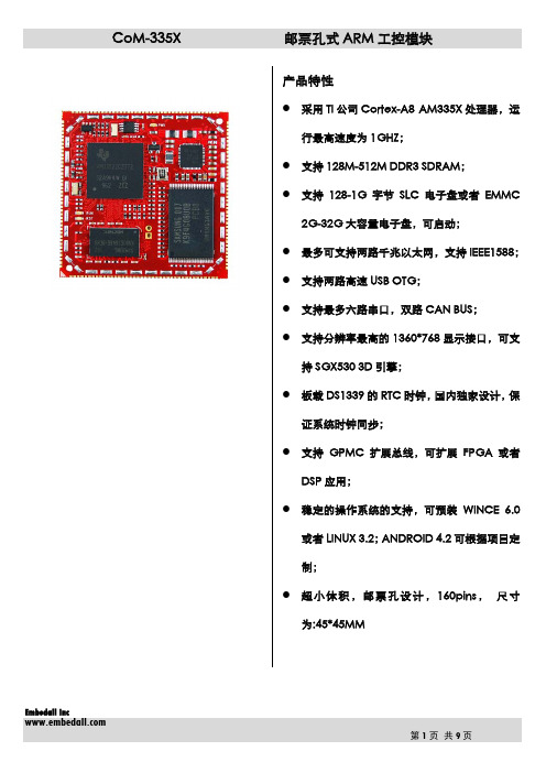
产品特性●采用TI公司Cortex-A8 AM335X处理器,运行最高速度为1GHZ;●支持128M-512M DDR3 SDRAM;●支持128-1G字节 SLC电子盘或者EMMC2G-32G大容量电子盘,可启动;●最多可支持两路千兆以太网,支持IEEE1588;●支持两路高速USB OTG;●支持最多六路串口,双路CAN BUS;●支持分辨率最高的1360*768显示接口,可支持SGX530 3D引擎;●板载DS1339的RTC时钟,国内独家设计,保证系统时钟同步;●支持GPMC扩展总线,可扩展FPGA或者DSP应用;●稳定的操作系统的支持,可预装WINCE 6.0或者LINUX 3.2;ANDROID 4.2可根据项目定制;●超小体积,邮票孔设计,160pins, 尺寸为:45*45MM简要介绍工业宽温设计,工作更稳定:CoM-335X Computer-on-Module (CoM),该产品集成了 ARM Cortex-A8 1GHz(MAX) TI AM335X 处理器,稳定运行WindowsCE 6.0 和Linux 3.2。
CoM-335X提供了3.3V I/O接口,可提供宽温的工业组件,运行于条件恶劣的工业现场!提供开发套件,可快速应用开发套件中包括主板、各种LCD配件,提供开发工具以及API函数、参考代码、详细的使用手册,让客户快速上手。
部件组成FUNCTION CoM-335X主控制器 TI Am335X,Cortex-A8,1GHZ(Max)内存256MB DDR3(最大可到512MB)闪存SLC NAND 128MB (最大到1GMB) 或者EMMC(最大到32GMB)图形显示 内置24位 LCD控制器主要参数时钟 DS1339U-33看门狗 有电源管理 TPS65217C (可支持电池供电的移动应用)复位 支持软件和硬件复位 (直接写寄存器)串口 串口6个,LVTTL电平以太网 2,10/100/1000MbpsUSB 2.0 Client1个,高速USB 2.0 Host 1个,高速SD/MMC卡 四线触摸屏 支持4线、5线、8线I/O系统总线 支持16位数据总线、12位地址总线,可支持接口FPGA或DSP(与24位LCD接口复用)IIC接口 2SPI接口 2GPIO 多个3.3V LVTTL电平MCASP音频 1CAN总线 2(与IIC复用一路)Graphic Chip支持2D/3D,仅对于AM3354多媒体分辨率最大1360×768LCD接口 16-bit TTL接口电源 5.0 V (+-5%)电源PowerTBDConsumption尺寸45MM*45MM*3.2MM尺寸 & 环境工作温度-20 ~ 70° C (可定制-40 ~85°C)工作湿度 5 ~ 95 % ,冷凝结RoHS YES其他认证CE软件支持Linux 3.2 (WCE6.0或者ANDROID项目定制支持)引脚定义支持软件订购信息Part No. CPU RAM FlashMemory UART LAN USBHostUSBOTGLCD videodecoderTouch SD IIC SPI EBI BUS PowerInputOperatingtemp.Com-335X-A1 AM3352 128M 256M 6 1 1 1 24-bit yes1 2 1 yes 5.0v 0-70 Com-335X-A2 AM3352 128M 256M 6 1 1 1 24-bit yes1 2 1 yes 5.0v -20-70 Com-335X-B1 AM3354 128M 256M 6 1 1 1 24-bit 3D yes 1 2 1 yes 5.0v -20-70 Com-335X-B2 AM3354 256M 256M 6 1 1 1 24-bit 3D yes 1 2 1 yes 5.0v -20-70Com-335X-C1 AM3352 512M EMMC2G 6 1 1 1 24-bit yes1 2 1 NO 5.0v -20-70Com-335X-C2 AM3352 512M EMMC4G 6 1 1 1 24-bit yes1 2 1 NO 5.0v -20-70Com-335X-D1 AM3354 512M EMMC2G6 1 1 1 24-bit 3D yes 1 2 1 NO 5.0v -20-70Com-335X-D2 AM3354 512M EMMC4G6 1 1 1 24-bit 3D yes 1 2 1 NO 5.0v -20-70尺寸(mm)评估套件推荐应用1.应用案例1-POS机2.应用案例2-监护仪3.应用案例3-人机界面。
飞凌嵌入式AM335x产品规格书-2014-09-18

第 3页
OK335x 产品规格书 2014-09-18
第一章 产品说明
1.1 产品总述
OK335x 系列产品是由飞凌自主设计、生产和发行销售的高性能,工业级开发平台。开 发平台采用了 TI 公司的 AM335X Cortex-A8 处理器,运行主频高达 1GHz,AM335X 处理器集 成了两个千兆网卡,集成了 CAN 总线控制器,IIC 控制器,LCD 控制器,集成了 PowerVR SGX530 图形处理器,非常适合工业控制,多媒体终端等应用领域。
第四章 OK335xS-II 产品................................................................................................................20 4.1 产品概述............................................................................................................................20 4.1.1 FET335xS-II 概述................................................................................................... 20 4.1.2 OK335xS-II 概述.....................................................................................................21 4.2 产品参数............................................................................................................................22 4.2.1 FET335xS-II 硬件参数........................................................................................... 22 4.2.2 FET335xS-II 软件参数........................................................................................... 22 4.2.3 OK335xS-II 接口说明............................................................................................24 4.3 OK335xS-II 尺寸说明....................................................................................................25 4.3.1 FET335xS-II 核心板尺寸说明图........................................................................... 25 4.3.2 OK335xS-II 底板尺寸说明图.................................................................................25
- 1、下载文档前请自行甄别文档内容的完整性,平台不提供额外的编辑、内容补充、找答案等附加服务。
- 2、"仅部分预览"的文档,不可在线预览部分如存在完整性等问题,可反馈申请退款(可完整预览的文档不适用该条件!)。
- 3、如文档侵犯您的权益,请联系客服反馈,我们会尽快为您处理(人工客服工作时间:9:00-18:30)。
基于AM335x的工业自动化应用
第1题:AM335x在工业驱动器的运用中,可提供几路PWM供客户使用?
A1路
B 2路
C 3路
D 4路
正确答案:C所选答案:A
第2题:下面哪些是AM335X适合的应用?
A I/O设备及传感器
B人机交互界面(HMI)
C PLC主站
D PLC从站
正确答案:A,B,C,D所选答案:A
第3题:对于操作系统的支持,AM335x现在可以提供的有哪些方案?
A WINCE
B LINUX
C ANDROID
D VXWORKS
正确答案:A,B,C所选答案:A
第4题:AM335X在HMI应用中使用的3D图形显示效果是由以下哪个模块来加速实现的?
A MPU
B PRU
C GPU
D PMU
正确答案:C所选答案:A
第5题:目前AM335x可以支持的启动模式有以下哪几种?
A NAND FLASH
B NOR FLASH
C SPI FLASH
D SD
正确答案:A,B,C,D所选答案:A
第1题:AM335x在工业驱动器的运用中,可提供几路PWM供客户使用?
A1路
B 2路
C 3路
D 4路
正确答案:C所选答案:A
第2题:对于需要使用3D加速特性以及EtherCAT从站通信时,可以选择的AM335x型号是以下哪种?
A AM3359
B AM3358
C AM3357
D AM3354
正确答案:A所选答案:A
第3题:下面哪些是AM335X适合的应用?
A I/O设备及传感器
B人机交互界面(HMI)
C PLC主站
D PLC从站
正确答案:A,B,C,D所选答案:A
第4题:AM335X在HMI应用中使用的3D图形显示效果是由以下哪个模块来加速实现的?
A MPU
B PRU
C GPU
D PMU
正确答案:C所选答案:A
第5题:AM335x可支持工业通信(EtherCAT等)的功能是由哪个模块实现的?
A MPU
B PRU
C GPU
D GPMC
正确答案:B所选答案:A
A VxWorks
B QNX
C SYS/BIOS
D TinyOS
正确答案:C所选答案:A
第2题:对于需要使用3D加速特性以及EtherCAT从站通信时,可以选择的AM335x型号是以下哪种?
A AM3359
B AM3358
C AM3357
D AM3354
正确答案:A所选答案:A
第3题:AM335x可提供的CAN通信接口数目是?
A1个
B 2个
C 3个
D 4个
正确答案:B所选答案:A
第4题:在工业通信的运用中,EtherCAT主站的实现可以由以下哪个模块完成?
A Ethernet
B CAN
C GPU
D PRU
正确答案:A,D所选答案:A
第5题:AM335x可支持工业通信(EtherCAT等)的功能是由哪个模块实现的?
A MPU
B PRU
C GPU
D GPMC
正确答案:B所选答案:A
A VxWorks
B QNX
C SYS/BIOS
D TinyOS
正确答案:C所选答案:C
第2题:在工业通信的运用中,EtherCAT主站的实现可以由以下哪个模块完成?
A Ethernet
B CAN
C GPU
D PRU
正确答案:A,D所选答案:D
第3题:AM335x可提供的CAN通信接口数目是?
A1个
B 2个
C 3个
D 4个
正确答案:B所选答案:B
第4题:AM335X在HMI应用中使用的3D图形显示效果是由以下哪个模块来加速实现的?
A MPU
B PRU
C GPU
D PMU
正确答案:C所选答案:C
第5题:对于需要使用3D加速特性以及EtherCAT从站通信时,可以选择的AM335x型号是以下哪种?
A AM3359
B AM3358
C AM3357
D AM3354
正确答案:A所选答案:A。