FPGA可编程逻辑器件芯片ADM1485ARZ-REEL中文规格书
FPGA可编程逻辑器件芯片5SGSED8N1F45C2L中文规格书

System OverviewThe processor core has three ports and can generate up to the following simultaneous off-core accesses per core clock cycle (CCLK):•One DMA data transfer through the D port•One L2 or external memory access through the P port•One MMR register access through the MMR portThe L2 or external memory access through the P port includes normal data or instruction access and cache read or write operation. System OverviewThe ADSP-BF54x processor processor system includes a Blackfin proces-sor core, a 128K byte level 2 (L2) memory, the peripheral set (seeFigure2-1 on page2-3), the external memory controller (EBIU, AMC and DDR), the DMA controllers, and bus interfaces.The external bus interface unit (EBIU) is the primary interface to the chip pins. Detailed information about the EBIU is discussed in “External Bus Interface Unit” on page5-1.P Port InterfaceFigure2-3 shows the interface between the processor core P port andmemory other than L1 through the 64-bit core L2 bus and shows theinterface between processor core P port and the EBIU through the 32-bit EAB bus.ADSP-BF54x Blackfin Processor Hardware ReferenceNFC Programming ExamplesP1 = (2048/256)(z);R3.L = lo(_Buffer);R3.H = hi(_Buffer);R4 = (2048/4)(z);R5 = 0x4(x);[P4 + (DMA22_START_ADDR - DMA22_CONFIG)] = R3;w[P4 + lo(DMA22_X_COUNT - DMA22_CONFIG)] = R4;w[P4 + lo(DMA22_X_MODIFY - DMA22_CONFIG)] = R5;R7 = 0x89(z);w[P4] = R7;LSETUP(_write_data_begin, _write_data_end) LC0 = P1;_write_data_begin:P1 = (256/4)(z);/* Reset the NFC */R7 = ECC_RST(z);w[P5 + lo(NFC_RST - NFC_CTL)] = R7;ssync;_wait_for_nfc_reset_completion:R7 = w[P5 + lo(NFC_RST - NFC_CTL)](z);CC = bittst(R7, bitpos(ECC_RST));_wait_for_nfc_reset_completion.END:if CC jump _wait_for_nfc_reset_completion;R7 = PG_WR_START(x);w[P5 + lo(NFC_PGCTL - NFC_CTL)] = R7;ADSP-BF54x Blackfin Processor Hardware Reference。
FPGA可编程逻辑器件芯片ADM202EARNZ-REEL中文规格书

ADM202E/ADM1181AFEATURESComplies with 89/336/EEC EMC directive ESD protection to IEC1000-4-2 (801.2) ±8 kV: contact discharge ±15 kV: air-gap discharge ±15 kV: human body modelEFT fast transient/burst immunity (IEC1000-4-4) Low EMI emissions (EN55022) 230 kbits/s data rate guaranteed TSSOP package optionUpgrade for MAX202E, 232E, LT1181AAPPLICATIONSGeneral-purpose RS-232 data link Portable instruments PDAsGENERAL DESCRIPTIONThe ADM202E and ADM1181A are robust, high speed, 2-channel RS-232/V .28 interface devices that operate from a single 5 V power supply. Both products are suitable for operation in harsh electrical environments and are compliant with the EU directive on EMC (89/336/EEC). Both the level of electromagnetic emissions and immunity are in compliance. EM immunity includes ESD protection in excess of ±15 kV on all I/O lines, fast transient/burst protection (1000-4-4), and radiated immunity (1000-4-3). EM emissions include radiated and conducted emissions as required by Information Technology Equipment EN55022, CISPR22.The ADM202E and ADM1181A conform to the EIA-232E and CCITT V .28 specifications and operate at data rates up to 230 kbps.Four external 0.1 µF charge-pump capacitors are used for the voltage doubler/inverter, permitting operation from a single 5 V supply.FUNCTIONAL BLOCK DIAGRAMS*INTERNAL 5k ΩPULL-DOWN RESISTOR ON EACH RS-232 INPUT10V T1T2R1R2*0.1µF 0.1µµF00066-001Figure 1.0.1µ 10V 10VT1µF T2R1R2*0.1µF 00066-002*INTERNAL 5k Ω PULL-DOWN RESISTOR ON EACH RS-232 INPUTFigure 2.The ADM202E provides a robust pin-compatible upgrade for existing ADM202, ADM232L, or MAX202E/MAX232E sockets. It is available in a 16-lead PDIP , a wide SOIC, a narrow SOIC, and a space-saving TSSOP package that is 44% smaller than the SOIC package.The ADM1181A provides a robust pin-compatible upgrade for the LTC1181A, and it is available in a 16-lead PDIP package and a wide 16-lead SOIC package.ADM202E/ADM1181A Rev. C | Page 6 of 16GENERAL DESCRIPTIONThe ADM202E/ADM1181E are rugged RS-232 linedrivers/receivers. Step-up voltage converters coupled with level-shifting transmitters and receivers allow RS-232 levels to be developed while operating from a single 5 V supply.Features include low power consumption, high transmission rates, and compliance with the EU directive on electromagnetic compatibility. EM compatibility includes protection against radiated and conducted interference, including high levels of electrostatic discharge.All inputs and outputs contain protection against electrostatic discharges of up to ±15 kV and electrical fast transients of up to ±2 kV . This ensures compliance to IEC1000-4-2 and IEC1000-4-4 requirements.The devices are ideally suited for operation in electrically harsh environments or where RS-232 cables are frequently being plugged/unplugged. They are also immune to high RF field strengths without special shielding precautions.CMOS technology is used to minimize the power dissipation, allowing maximum battery life in portable applications. The ADM202E/ADM1181A serve as a modification,enhancement, and improvement to the ADM230–ADM241 family and its derivatives. It is essentially plug-in compatible and do not have materially different applications.CIRCUIT DESCRIPTIONThe internal circuitry consists of four main sections: • A charge-pump voltage converter • 5 V logic to EIA-232 transmitters •EIA-232 to 5 V logic receivers.•Transient protection circuit on all I/O linesCharge-Pump DC-to-DC Voltage ConverterThe charge-pump voltage converter consists of a 200 kHz oscillator and a switching matrix. The converter generates a ±10 V supply from the input 5 V level. This is done in two stages, using a switched capacitor technique, as illustrated in Figure 6 and Figure 7. First, the 5 V input supply is doubled to 10 V , using Capacitor C1 as the charge storage element. The 10 V level is then inverted to generate −10 V , using C2 as the storage element. Capacitor C3 and Capacitor C4 are used to reduce the output ripple. Their values are not critical and can be increased if desired. On the ADM202E, Capacitor C3 is shown connected between V+ and V CC , whereas it is connected between V+ and GND on the ADM1181A. It is acceptable to use eitherconfiguration with both the ADM202E and ADM1181A. Ifdesired, larger capacitors (up to 47 µF) can be used forCapacitor C1 to Capacitor C4. This facilitates direct substitution with older generation charge-pump RS-232 transceivers.CCCCNOTE: C3 CONNECTS BETWEEN V+ AND GND ON THE ADM1181A00066-006Figure 6. Charge-Pump Voltage DoublerFigure 7. Charge-Pump Voltage InverterTransmitter (Driver) SectionThe drivers convert 5 V logic input levels into RS-232 output levels. When driving an RS-232 load with V CC = 5 V , the output voltage swing is typically ±9 V .Receiver SectionThe receivers are inverting level shifters that accept RS-232 input levels and translate them into 5 V logic output levels. The inputs have internal 5 kΩ pull-down resistors to ground and are also protected against overvoltages of up to ±30 V . Unconnected inputs are pulled to 0 V by the internal 5 kΩ pull-down resistor. Therefore, unconnected inputs and those connected to GND have a Logic 1 output level.The receivers have Schmitt-trigger inputs with a hysteresis level of 0.65 V . This ensures error-free reception for both noisy inputs and inputs with slow transition times.HIGH BAUD RATEThe ADM202E/ADM1181A feature high slew rates, permitting data transmission at rates well in excess of the EIA/RS-232-E specifications. RS-232 voltage levels are maintained at data rates of up to 230 kbps, even under worst case loading conditions. This allows for high speed data links between two terminals and is also suitable for the new generation ISDN modem standards, which require data rates of 230 kbps. The slew rate is internally controlled to less than 30 V/µs to minimize EMI interference.ADM202E/ADM1181ARev. C | Page 7 of 16ADM202E/ADM1181ARev. C | Page 10 of 16ESD TESTING (IEC1000-4-2)IEC1000-4-2 (previously 801-2) specifies compliance testing using two coupling methods, contact discharge and air-gap discharge. Contact discharge calls for a direct connection to the unit being tested. Air-gap discharge uses a higher test voltage, but does not make direct contact with the unit being tested. With air-gap discharge, the discharge gun is moved toward the unit being tested, developing an arc across the air gap. This method is influenced by humidity, temperature, barometric pressure, distance, and rate of closure of the discharge gun. Although less realistic, the contact-discharge method is more repeatable and is gaining preference to the air-gap method. Although very little energy is contained within an ESD pulse, the extremely fast rise time coupled with high voltages can cause failures in unprotected semiconductors. Catastrophic destruction can occur immediately as a result of arcing orheating. Even if catastrophic failure does not occur immediately, the device might suffer from parametric degradation, which can result in degraded performance. The cumulative effects of continuous exposure can eventually lead to complete failure. I/O lines are particularly vulnerable to ESD damage. Simply touching or plugging in an I/O cable can result in a static discharge, which can damage or completely destroy theinterface product connected to the I/O port. Traditional ESD test methods, such as the MIL-STD-883B method 3015.7, do not fully test a product’s susceptibility to this type of discharge. This test was intended to test a product’s susceptibility to ESD damage during handling. Each pin is tested with respect to all other pins. There are some important differences between the traditional test and the IEC test: •The IEC test is much more stringent in terms of discharge energy. The injected peak current is over four times greater. •The current rise time is significantly faster in the IEC test.•The IEC test is carried out while power is applied to the device.It is possible that the ESD discharge could induce latch-up in the device being tested. Therefore, this test is more representative of a real-world I/O discharge where the equipment is operating normally with power applied. For peace of mind, however, both tests should be performed to ensure maximum protection during both handling and field service.ESD TEST METHOD R2C1H.BODY MIL-STD883B 1.5k Ω100pF IEC1000-4-2330Ω150pF00066-018Figure 18. ESD Test StandardsI P E A K (%)00066-019Figure 19. Human Body Model ESD Current WaveformFigure 20. IEC1000-4-2 ESD Current WaveformThe ADM202E/ADM1181E products are tested using both of the previously mentioned test methods. Pins are tested with respect to all other pins as per the MIL-STD-883B specification. In addition, I/O pins are tested as per the IEC test specification. The products were tested under the following conditions: •Power-On •Power-OffThere are four levels of compliance defined by IEC1000-4-2. The ADM202E/ADM1181A products meet the most stringent level of compliance both for contact and for air-gap discharge. This means that the products are able to withstand contact discharges in excess of 8 kV and air-gap discharges in excess of 15 kV .ADM202E/ADM1181ARev. C | Page 11 of 16Table 4. IEC1000-4-2 Compliance LevelsLevel Contact Discharge Air Discharge 1 2 kV 2 kV 2 4 kV 4 kV 3 6 kV 8 kV 48 kV15 kVTable 5. ADM202E/ADM1181A ESD Test ResultsESD Test Method I/O Pins MIL-STD-883B ±15 kV IEC1000-4-2 Contact ±8 kV Air±15 kVFAST TRANSIENT/BURST TESTING (IEC1000-4-4)IEC1000-4-4 (previously 801-4) covers electrical fast transient (EFT)/burst immunity. Electrical fast transients occur as a result of arcing contacts in switches and relays. The tests simulate the interference generated when, for example, a power relaydisconnects an inductive load. A spark is generated due to the well-known back EMF effect. In fact, the spark consists of a burst of sparks as the relay contacts separate. The voltageappearing on the line, therefore, consists of a burst of extremely fast transient impulses. A similar effect occurs when switching on fluorescent lights.The fast transient/burst test defined in IEC1000-4-4 simulates this arcing, and its waveform is illustrated in Figure 17. It consists of a burst of 2.5 kHz to 5 kHz transients repeating at300 ms intervals. It is specified for both power and data lines.00066-021Figure 21. IEC1000-4-4 Fast Transient WaveformA simplified circuit diagram of the actual EFT generator is illustrated in Figure 22.The transients are coupled onto the signal lines using an EFT coupling clamp. The clamp, which is 1 m long, completelysurrounds the cable, providing maximum coupling capacitance (50 pF to 200 pF typ) between the clamp and the cable. High energy transients are capacitively coupled to the signal lines. Fast rise times (5 ns), as specified by the standard, result in very effective coupling. This test is very strenuous because high voltages are coupled onto the signal lines. The repetitive transients often cause problems where single pulses do not. Destructive latch-up can be induced due to the high energy content of the transients. Note that this stress is applied while the interface products are powered up and transmitting data. The EFT test applieshundreds of pulses with higher energy than ESD. Worst-case transient current on an I/O line can be as high as 40 A.00066-022Figure 22. IEC1000-4-4 Fast Transient GeneratorTest results are classified according to the following: •Classification 1: Normal performance within specifi- cation limits•Classification 2: Temporary degradation or loss of performance that is self-recoverable•Classification 3: Temporary degradation or loss of function or performance that requires operator intervention or system reset•Classification 4: Degradation or loss of function that is not recoverable due to damageThe ADM202E/ADM1181A meet Classification 2 and have been tested under worst-case conditions using unshielded cables. Data transmission during the transient condition iscorrupted, but can resume immediately following the EFT event without user intervention.。
FPGA可编程逻辑器件芯片AD8694ARUZ-REEL中文规格书

INPUT CAPACITANCE Common-Mode Input Capacitance Differential Input Capacitance
OUTPUT CHARACTERISTICS Output Voltage High
RL = 2 kΩ, VO = 0.5 V to 2.2 V RL = 2 kΩ, VO = 0.5 V to 2.2 V
CCM CDM
VOH
IL = 1 mA
−40°C < TA < +125°C
VOL
IL = 1 mA
−40°C < TA < +125°C
ISC
ZOUT
f = 1 MHz, AV = 1
Table 1. Parameter INPUT CHARACTERISTICS
Offset Voltage
Input Bias Current
Input Offset Current
Input Voltage Range Common-Mode Rejection Ratio
Large Signal Voltage Gain AD8691/AD8692 AD8694
APPLICATIONS
Photodiode amplification Battery-powered instrumentation Medical instruments Multipole filters Sensors Portable audio devices
GENERAL DESCRIPTION
NOISE PERFORMANCE Voltage Noise Voltage Noise Density
MEMORY存储芯片ADM485ARZ-REEL中文规格书
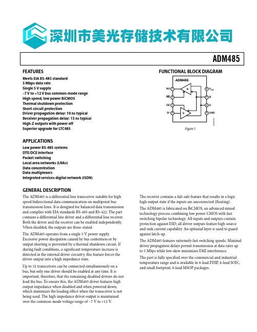
ADM485FUNCTIONAL BLOCK DIAGRAMCC 00078-001FEATURESMeets EIA RS-485 standard 5 Mbps data rateSingle 5 V supply–7 V to +12 V bus common-mode range High speed, low power BiCMOS Thermal shutdown protection Short-circuit protectionDriver propagation delay: 10 ns typical Receiver propagation delay: 15 ns typical High-Z outputs with power off Superior upgrade for LTC485APPLICATIONSLow power RS-485 systems DTE/DCE interface Packet switchingLocal area networks (LNAs) Data concentration Data multiplexersIntegrated services digital network (ISDN)GENERAL DESCRIPTIONThe ADM485 is a differential line transceiver suitable for high speed bidirectional data communication on multipoint bus transmission lines. It is designed for balanced data transmission and complies with EIA standards RS-485 and RS-422. The part contains a differential line driver and a differential line receiver. Both the driver and the receiver can be enabled independently. When disabled, the outputs are three-stated.The ADM485 operates from a single 5 V power supply. Excessive power dissipation caused by bus contention or by output shorting is prevented by a thermal shutdown circuit. If during fault conditions, a significant temperature increase is detected in the internal driver circuitry, this feature forces the driver output into a high impedance state.Up to 32 transceivers can be connected simultaneously on a bus, but only one driver should be enabled at any time. It is important, therefore, that the remaining disabled drivers do not load the bus. To ensure this, the ADM485 driver features high output impedance when disabled and when powered down, which minimizes the loading effect when the transceiver is not being used. The high impedance driver output is maintained over the common-mode voltage range of −7 V to +12 V .Figure 1.The receiver contains a fail-safe feature that results in a logic high output state if the inputs are unconnected (floating). The ADM485 is fabricated on BiCMOS, an advanced mixed technology process combining low power CMOS with fast switching bipolar technology. All inputs and outputs contain protection against ESD; all driver outputs feature high source and sink current capability. An epitaxial layer is used to guard against latch-up.The ADM485 features extremely fast switching speeds. Minimal driver propagation delays permit transmission at data rates up to 5 Mbps while low skew minimizes EMI interference. The part is fully specified over the commercial and industrial temperature range and is available in 8-lead PDIP , 8-lead SOIC, and small footprint, 8-lead MSOP packages.ADM485Rev. F | Page 2 of 16ADM485SPECIFICATIONSV CC = 5 V ± 5%, all specifications T MIN to T MAX, unless otherwise noted.Rev. F | Page 3 of 16ADM485TIMING SPECIFICATIONSV CC = 5 V ± 5%, all specifications T MIN to T MAX, unless otherwise noted.1 Guaranteed by characterization.Rev. F | Page 4 of 16ADM485Rev. F | Page 5 of 16ABSOLUTE MAXIMUM RATINGST A = 25°C, unless otherwise noted.Stresses above those listed under Absolute Maximum Ratings may cause permanent damage to the device. This is a stress rating only; functional operation of the device at these or any other conditions above those indicated in the operationalsection of this specification is not implied. Exposure to absolute maximum rating conditions for extended periods may affect device reliability.Table 4. TransmittingInputsOutputsDE DIB A 1 1 0 1 1 0 1 0 0X 1Z 2Z 21 X = don’t care.2Z = high impedance.1 X = don’t care.2Z = high impedance.ESD CAUTION。
FPGA可编程逻辑器件芯片5SGXMB5R1F43C1N中文规格书

Features for floating-point arithmetic:• A completely hardened architecture that supports multiplication, addition, subtraction, multiply-add, and multiply-subtract•Multiplication with accumulation capability and a dynamic accumulator reset control•Multiplication with cascade summation capability•Multiplication with cascade subtraction capability•Complex multiplication•Direct vector dot product•Systolic FIR filterTable 15.Variable-Precision DSP Block Configurations for Intel Arria 10 Devices Usage Example Multiplier Size (Bit)DSP Block Resources Medium precision fixed point Two 18 x 191One 27 x 271 High precision fixed or Single precisionfloating pointFixed point FFTs One 19 x 36 with external adder1Very high precision fixed point One 36 x 36 with external adder2Double precision floating point One 54 x 54 with external adder4Table 16.Resources for Fixed-Point Arithmetic in Intel Arria 10 DevicesThe table lists the variable-precision DSP resources by bit precision for each Intel Arria 10 device.The fractional synthesis PLLs support the following features:•Reference clock frequency synthesis for transceiver CMU and Advanced Transmit (ATX) PLLs•Clock network delay compensation•Zero-delay buffering•Direct transmit clocking for transceivers•Independently configurable into two modes:—Conventional integer mode equivalent to the general purpose PLL—Enhanced fractional mode with third order delta-sigma modulation•PLL cascadingI/O PLLsThe integer mode I/O PLLs are located in each bank of 48 I/Os. You can use the I/OPLLs to simplify the design of external memory and high-speed LVDS interfaces.In each I/O bank, the I/O PLLs are adjacent to the hard memory controllers and LVDSSERDES. Because these PLLs are tightly coupled with the I/Os that need to use them,it makes it easier to close timing.You can use the I/O PLLs for general purpose applications in the core such as clocknetwork delay compensation and zero-delay buffering.Intel Arria 10 devices support PLL-to-PLL cascading.FPGA General Purpose I/OIntel Arria 10 devices offer highly configurable GPIOs. Each I/O bank contains 48general purpose I/Os and a high-efficiency hard memory controller.The following list describes the features of the GPIOs:•Consist of 3 V I/Os for high-voltage application and LVDS I/Os for differential signaling—Up to two 3 V I/O banks, available in some devices, that support up to 3 V I/O standards—LVDS I/O banks that support up to 1.8 V I/O standards•Support a wide range of single-ended and differential I/O interfaces•LVDS speeds up to 1.6 Gbps•Each LVDS pair of pins has differential input and output buffers, allowing you to configure the LVDS direction for each pair.•Programmable bus hold and weak pull-up•Programmable differential output voltage (V OD) and programmable pre-emphasis。
FPGA可编程逻辑器件芯片5AGXMA5G4F35I5N中文规格书

Chapter 4:TriMatrix Embedded Memory Blocks in Stratix III DevicesOverviewTrue Dual-Port ModeStratix III M9K and M144K blocks support true dual-port mode. Sometimes calledbi-directional dual-port, this mode allows you to perform any combination of twoport operations: two reads, two writes, or one read and one write at two differentclock frequencies. Figure4–15 shows the true dual-port RAM configuration.Figure4–15.Stratix III True Dual-Port Memory (Note1)Note to Figure4–15:(1)True dual-port memory supports input/output clock mode in addition to the independent clock mode shown.The widest bit configuration of the M9K and M144K blocks in true dual-port mode isas follows:■512 × 16-bit (×18-bit with parity) (M9K)■4K × 32-bit (×36-bit with parity) (M144K)Wider configurations are unavailable because the number of output drivers isequivalent to the maximum bit width of the respective memory block. Because truedual-port RAM has outputs on two ports, its maximum width equals half of the totalnumber of output drivers. Table4–7 lists the possible M9K block mixed-port widthconfigurations in true dual-port mode.Table4–7.Stratix III M9K Block Mixed-Width Configuration (True Dual-Port Mode)Stratix III Device Handbook, Volume 1Chapter 3:MultiTrack Interconnect in Stratix III DevicesI/O Block Connections to Interconnect Figure3–9.Row I/O Block Connection to InterconnectStratix III Device Handbook, Volume 1Chapter 1:Stratix III Device Family OverviewReference and Ordering Information Stratix III Device Handbook, Volume 1Signal IntegrityStratix III devices simplify the challenge of signal integrity through a number of chip, package, and board level enhancements to enable efficient high-speed data transfer into and out of the device. These enhancements include:■8:1:1 user I/O/Gnd/V CC ratio to reduce the loop inductance in the package ■Dedicated power supply for each I/O bank, limit of I/Os is 24 to 48 I/Os per bank,to help limit simultaneous switching noise■Programmable slew-rate support with up to four settings to match desired I/Ostandard, control noise, and overshoot■Programmable output-current drive strength support with up to six settings tomatch desired I/O standard performance■Programmable output-delay support to control rise/fall times and adjust dutycycle, compensate for skew, and reduce simultaneous switching outputs (SSO)noise■Dynamic OCT with auto calibration support for series and parallel OCT anddifferential OCT support for LVDS I/O standard on the left/right banks fFor more information about SI support in the Quartus II software, refer to the Quartus II Handbook .f For more information about how to use the various configuration, PLL, externalmemory interfaces, I/O, high-speed differential I/O, power, and JTAG pins, refer to the Stratix III Device Family Pin Connection Guidelines .Reference and Ordering InformationThe following section describes Stratix III device software support and orderinginformation.Software SupportStratix III devices are supported by the Altera Quartus II design software, version 6.1 and later, which provides a comprehensive environment forsystem-on-a-programmable-chip (SOPC) design. The Quartus II software includes HDL and schematic design entry, compilation and logic synthesis, full simulation and advanced timing analysis, SignalTap ®II logic analyzer, and device configuration.f For more information about the Quartus II software features, refer to the Quartus IIHandbook .The Quartus II software supports a variety of operating systems. The specificoperating system for the Quartus II software can be obtained from the Quartus IIReadme.txt file or the Operating System Support section of the Altera website. It also supports seamless integration with industry-leading EDA tools through theNativeLink ® interface.。
FPGA可编程逻辑器件芯片EP2AGX65DF25C4N中文规格书

When the host moves to the status stage of the request, another endpoint 0 interrupt will be generated to indicate that the request has completed. No further action is required from the software-the interrupt is just a confirmation that the request completed successfully.If the command is an unrecognized command, or for some other reason cannot be executed, then when it has been decoded, the USB_EP0_CSRn_P register should be written to set the USB_EP0_CSRn_P.SPKTRDY bit and to set the USB_EP0_CSRn_P.SENDSTALL bit. When the host requests data, the USB controller will send a stall to tell the host that the request was not executed. An endpoint 0 interrupt will be generated and the USB_EP0_CSRn_P.SENTSTALL bit is set.If the host requests more data after USB_EP0_CSRn_P.DATAEND has been set, then the USB controller sendsa stall. An endpoint 0 interrupt is generated and the USB_EP0_CSRn_P.SENTSTALL bit is set.Zero Data RequestsZero data requests have all their information included in the 8-byte command and require no additional data to be transferred.Examples of zero data standard device requests are: SET_FEATURE, CLEAR_FEATURE, SET_ADDRESS, SET_CONFIGURATION, and SET_INTERFACE.As with all requests, the sequence of events begins when the software receives an endpoint 0 interrupt. The USB_EP0_CSRn_P.RXPKTRDY bit will also have been set. The 8-byte command should then be read from the endpoint 0 FIFO, decoded and the appropriate action taken. For example if the command is SET_ ADDRESS, the 7-bit address value contained in the command is written to the USB_FADDR register.The USB_EP0_CSRn_P.SPKTRDY bit should be set (indicating that the command is read from the FIFO) and the USB_EP0_CSRn_P.DATAEND bit should be set (indicating that no further data is expected for thisrequest).When the host moves to the status stage of the request, a second endpoint 0 interrupt is generated, indi-cating that the request has completed. No further action is required from the software—the second inter-rupt is just a confirmation that the request completed successfully.If the command is an unrecognized command, or for some other reason cannot be executed, then when it is decoded, the USB_EP0_CSRn_P.SPKTRDY bit is set which sets the USB_EP0_CSRn_P.SENDSTALL bit.When the host moves to the status stage of the request, the USB controller sends a stall to tell the host that the request was not executed. A second endpoint 0 interrupt is generated and the USB_EP0_CSRn_P.SENTSTALL bit is set.If the host sends more data after the USB_EP0_CSRn_P.DATAEND bit is set, then the USB controller sends a stall. An endpoint 0 interrupt is generated and the USB_EP0_CSRn_P.SENTSTALL bit is set.ENDPOINT 0 StatesWhen the USB is operating as a peripheral, the Endpoint 0 control needs three modes (IDLE, TX and RX) corresponding to the different phases of the control transfer and the states Endpoint 0 enters for thedifferent phases of the transfer. (See Endpoint 0 Service Routine as Peripheral.)TXMAXP.MULTM1 bits to set the maximum number of such packets that can be sent in one micro-frame (2 or 3). Together, these set the maximum size of packet that can be loaded into the FIFO.At least one USB packet always is sent. The number of further USB packets sent in the same micro-frame depends on the amount of data loaded into the FIFO. The USB_EPn_TXCSR_P.TXPKTRDY bit is cleared and an interrupt is generated only when all the packets have been sent. Each USB packet is sent in response to an IN token. If, at the end of a micro-frame, the USB controller has not received enough IN tokens to send all the USB packets (for example, because one of the IN tokens received was corrupted), the remaining data is flushed from the FIFO. The USB_EPn_TXCSR_P.TXPKTRDY bit is cleared and the USB_EPn_TXCSR_P.INCOMPTX bit is set to indicate that not all of the data loaded into the FIFO was sent.High Bandwidth Isochronous/Interrupt OUT EndpointsIn high-speed mode, isochronous receive endpoints can receive up to three USB packets in anymicro-frame, with a payload of up to 1024 bytes in each packet, corresponding to a data transfer rate of up to 3072 bytes per micro-frame. High-bandwidth interrupt transactions can similarly be received in host mode, but there is no support for high-bandwidth interrupt transactions in peripheral mode.The High Bandwidth OUT Endpoints figure shows an overview of high-bandwidth OUT endpoints.The USB controller supports this rate by automatically combining all the USB packets received during a micro-frame into a single packet of up to 3 normal packets in size within the receive FIFO. From the point of view of the software in the processor core, the operation is then exactly as described as for single or double packet buffering (as appropriate), except the USB_EPn_RXCSR_P.RXPKTRDY bit always needs to be cleared manually (for example by the processor core) because the auto-clear function does not operate with high-bandwidth isochronous transfers.The maximum number of USB packets that may be received in any micro-frame and the maximumpayload of these packets are configured using the USB_EPn_RXMAXP.MAXPAY bits to set the maximumpayload in any USB packet and the USB_EPn_RXMAXP.MULTM1 bits to set the maximum number of these packets that may be received in a micro-frame (2 or 3).U NIVERSAL S ERIAL B US (USB)USB O PERATING M ODESFigure 22-6:Endpoint 0 Idle Mode (Setup Phase)TX ModeAs shown in the Endpoint 0 TX Mode figure when the endpoint is in TX state, all arriving IN tokens need to be treated as part of a data phase until the required amount of data has been sent to the host. If either a SETUP or an OUT token is received while the endpoint is in the TX state, a USB_EP0_CSRn_P.SETUPEND condition occurs since the core expects only IN tokens.Three events can cause the TX mode to terminate before the expected amount of data has been sent:•The host sends an invalid token which sets the USB_EP0_CSRn_P.SETUPEND bit.•The firmware sends a packet containing less than the maximum packet size for endpoint 0.。
FPGA可编程逻辑器件芯片5SEEBF45I3L中文规格书

Dynamic Power Management ControllerADSP-BF54x Blackfin Processor Hardware ReferenceDynamic Power Management Controller States Power management states are synonymous with the PLL control state. The active and full on states of the DPMC/PLL can be determined by reading the PLL status register (see “PLL Status (PLL_STAT) Register” on page 18-27). In these modes, the core can either execute instructions or be in the idle core state. If the core is in the Idle state, it can be awakened by several sources.The following sections describe the DPMC/PLL states in more detail, as they relate to the power management controller functions.Full On ModeFull on mode is the maximum performance mode. In this mode, the PLL is enabled and not bypassed. Full on mode is the normal execution state of the processor, with the processor and all enabled peripherals running at full speed. The system clock (SCLK ) frequency is determined by the SSEL -specified ratio to VCO . DMA access is available to L1 and external memories. From full on mode, the processor can transition directly to active, sleep, or deep sleep modes, as shown in Figure 18-2 on page 18-12.Table 18-4. Operational Characteristics OperatingModePower Savings PLL CCLK SCLK Allowed DMA Access Status Bypassed Full OnNone Enabled No Enabled Enabled L1ActiveMedium Enabled 1Yes Enabled Enabled L1SleepHigh Enabled No Disabled Enabled –Deep Sleep Maximum Disabled –Disabled Disabled –1 PLL can also be disabled in this mode.Dynamic Power Management ControllerDynamic Supply Voltage ControlIn addition to clock frequency control, the processor provides the capabil-ity to run the core processor at different voltage levels. As powerdissipation is proportional to the voltage squared, significant power reduc-tions can be accomplished when lower voltages are used.The processor uses multiple power domains. Each power domain has a separate V DD supply. Note that the internal logic of the processor and much of the processor I/O can be run over a range of voltages. SeeADSP-BF542/544/547/548/549 Embedded Processor Data Sheet for details on the allowed voltage ranges for each power domain and power dissipa-tion data.Power Supply ManagementThe processor provides an on-chip switching regulator controller which, with some external hardware, can generate internal voltage levels from the external V DDEXT supply with an external power transistor as shown in Figure18-3. This voltage level can be reduced to save power, depending upon the needs of the system.ADSP-BF54x Blackfin Processor Hardware Reference。
- 1、下载文档前请自行甄别文档内容的完整性,平台不提供额外的编辑、内容补充、找答案等附加服务。
- 2、"仅部分预览"的文档,不可在线预览部分如存在完整性等问题,可反馈申请退款(可完整预览的文档不适用该条件!)。
- 3、如文档侵犯您的权益,请联系客服反馈,我们会尽快为您处理(人工客服工作时间:9:00-18:30)。
Data SheetADE7758MCU04443-086Figure 87. ADE7758 Interrupt Management04443-087Figure 88. ADE7758Interrupt TimingDINDOUT04443-088Figure 89. Addressing ADE7758 Registers via the Communications RegisterThe communications register is an 8-bit, write-only register. The MSB determines whether the next data transfer operation is a read or a write. The seven LSBs contain the address of the register to be accessed (see Table 16).Figure 90 and Figure 91 show the data transfer sequences for a read and write operation, respectively.MULTIBYTEDIN SCLKDOUTREAD DATACS 04443-089Figure 90. Reading Data from the ADE7758 via the Serial InterfaceDINSCLKCS04443-090Figure 91. Writing Data to the ADE7758 via the Serial InterfaceOn completion of a data transfer (read or write), the ADE7758 once again enters into communications mode, that is, the next instruction followed must be a write to the communications register.A data transfer is completed when the LSB of the ADE7758 register being addressed (for a write or a read) is transferred to or from the ADE7758.SERIAL WRITE OPERATIONThe serial write sequence takes place as follows. With theADE7758 in communications mode and the CS input logic low, a write to the communications register takes place first. The MSB of this byte transfer must be set to 1, indicating that the next data transfer operation is a write to the register. The seven LSBs of this byte contain the address of the register to be written to. The starts shifting in the register data on the next falling edge of SCLK. All remaining bits of register data are shifted in on the falling edge of the subsequent SCLK pulses (see ).ADE7758Figure 92As explained earlier, the data write is initiated by a write to the communications register followed by the data. During a data write operation to the ADE7758, data is transferred to all on-chip registers one byte at a time. After a byte is transferred into the serial port, there is a finite time duration before the content in the serial port buffer is transferred to one of the ADE7758 on-chip registers. Although another byte transfer to the serial port can start while the previous byte is being transferred to the destination register, this second-byte transfer should not finish until at least 900 ns after the end of the previous byte transfer. This functionality is expressed in the timing specification t 6 (see Figure 92). If a write operation is aborted during a byte transfer (CS brought high), then that byte is not written to the destination register.Destination registers can be up to 3 bytes wide (see theAccessing the On-Chip Registers section). Therefore, the first byte shifted into the serial port at DIN is transferred to the most significant byte (MSB) of the destination register. If the destination register is 12 bits wide, for example, a two-byte data transfer must take place. The data is always assumed to be right justified; therefore, in this case, the four MSBs of the first byte would be ignored, and the four LSBs of the first byte written to the ADE7758 would be the four MSBs of the 12-bit word. Figure 93 illustrates this example.COMMAND BYTE MOST SIGNIFICANT BYTE LEAST SIGNIFICANT BYTE04443-091Figure 92. Serial Interface Write Timing DiagramSCLKDIN X X X X DB11DB10DB9DB8DB7DB6DB5DB4DB3DB2DB1DB0MOST SIGNIFICANT BYTE LEAST SIGNIFICANT BYTE04443-092Figure 93. 12-Bit Serial Write OperationSCLKCSDINDOUTCOMMAND BYTE04443-093Figure 94. Serial Interface Read Timing DiagramOPERATIONAL MODE REGISTER (0x13)The general configuration of the ADE7758 is defined by writing to the OPMODE register. Table 18 summarizes the functionality of each bit in the OPMODE register.Table 18. OPMODE RegisterBit Location BitMnemonicDefaultValue Description0 DISHPF 0 The HPFs in all current channel inputs are disabled when this bit is set.1 DISLPF 0 The LPFs after the watt and VAR multipliers are disabled when this bit is set.2 DISCF 1 The frequency outputs APCF and VARCF are disabled when this bit is set.3 to 5 DISMOD 0 By setting these bits, the ADE7758 ADCs can be turned off. In normal operation, these bits shouldbe left at Logic 0.DISMOD[2:0] Description0 0 0 Normal operation.1Redirect the voltage inputs to the signal paths for the current channels andthe current inputs to the signal paths for the voltage channels.0 0 1 Switch off only the current channel ADCs.11Switch off current channel ADCs and redirect the current input signals to thevoltage channel signal paths.0 1 0 Switch off only the voltage channel ADCs.11Switch off voltage channel ADCs and redirect the voltage input signals to thecurrent channel signal paths.11PuttheADE7758 in sleep mode.111PuttheADE7758 in power-down mode (reduces AI DD to 1 mA typ).6 SWRST 0 Software Chip Reset. A data transfer to the ADE7758 should not take place for at least 166 μs aftera software reset.7 Reserved 0 This should be left at 0.MEASUREMENT MODE REGISTER (0x14)The configuration of the PERIOD and peak measurements made by the ADE7758 is defined by writing to the MMODE register. Table 19 summarizes the functionality of each bit in the MMODE register.Table 19. MMODE RegisterBit Location BitMnemonicDefaultValue Description0 to 1 FREQSEL 0 These bits are used to select the source of the measurement of the voltage line frequency.FREQSEL1 FREQSEL0 Source0 0 Phase A0 1 Phase B1 0 Phase C1 1 Reserved2 to 4 PEAKSEL 7 These bits select the phases used for the voltage and current peak registers. Setting Bit 2 switchesthe IPEAK and VPEAK registers to hold the absolute values of the largest current and voltagewaveform (over a fixed number of half-line cycles) from Phase A. The number of half-line cycles isdetermined by the content of the LINECYC register. At the end of the LINECYC number of half-linecycles, the content of the registers is replaced with the new peak values. Similarly, setting Bit 3 turnson the peak detection for Phase B, and Bit 4 for Phase C. Note that if more than one bit is set, theVPEAK and IPEAK registers can hold values from two different phases, that is, the voltage andcurrent peak are independently processed (see the Peak Current Detection section).5 to 7 PKIRQSEL 7 These bits select the phases used for the peak interrupt detection. Setting Bit 5 switches on themonitoring of the absolute current and voltage waveform to Phase A. Similarly, setting Bit 6 turns onthe waveform detection for Phase B, and Bit 7 for Phase C. Note that more than one bit can be set fordetection on multiple phases. If the absolute values of the voltage or current waveform samples inthe selected phases exceeds the preset level specified in the VPINTLVL or IPINTLVL registers thecorresponding bit(s) in the STATUS registers are set (see the Peak Current Detection section).Data Sheet ADE7758ADE7758 Data SheetCOMPUTATIONAL MODE REGISTER (0x16)The computational method of the ADE7758 is defined by writing to the COMPMODE register. Table 21 summarizes the functionality of each bit in the COMPMODE register.。