专用集成电路设计大作业
专用集成电路作业

Assignment 21. Give a descriptive definition for each of the following terms.(1) Starting substrate(2) Active region: The regions between these thick SiO 2 layers(3) LOCOS process: LOCal Oxidation of Silicon(1) Field oxide layer: 重掺杂硅区上均生长一层厚的氧化层(2) Shallow Trench Isolation (STI): an integrated circuit feature which prevents electricalcurrent leakage between adjacent semiconductor device components(3) Positive resist : a type of photoresist in which the portion of the photoresist that is exposedto light becomes soluble to the photoresist developernegative resist: a type of photoresist in which the portion of the photoresist that is exposed to light becomes insoluble to the photoresist developer(4) Sputtering: a process whereby atoms are ejected from a solid target material due tobombardment of the target by energetic particles(5) Reactive ion etching: an etching technology that High-energy ions from the plasma,generated under low pressure (vacuum) by an electromagnetic field, attack the wafer surface and react with it(6) Strong inversion layer: 半导体表面的少数载流子浓度等于体内的多数载流子浓度时, 半导体表面形成的一种表面势近似为不变的数值,耗尽层电荷及耗尽层厚度有极大值状态称为强反型态。
集成电路设计作业三

模拟cmos 集成电路设计作业三1. 如图所示,根据Vout 处来计算输出阻抗。
在Vout 看向上面的几个mos 管可以发现,无论哪一支路,四个管子的电流都会受到影响。
那么可以得到)1||1||1||1(654311m m m m m out m v g g g g g R g A ⨯===3161m m g g221324R KTV out n = 还有A 已经求得,故可以根据Pout 反推回到Pin 进而求得输入噪声功率为)62(324213121m m m in n g g g KT V +=2. (a )已知电阻噪声R KT I n /42= 且mos 管的噪声γ224m n KTg I =其中的y 取为常数2/3 那么两式子联立324542m KTg R KT = 求得gm=4103-⨯ 又知道gm=D oxn I LWC μ2 其中计算Cox已知tox=50的时候 对应的Cox 然后tox 为90的时候可以得到 Cox=3.83fF那么 代入得到方程x ⨯⨯⨯⨯⨯⨯=⨯-----4121544105101083.310350103 其中x 为所求的尺寸,代入得到 x=1.34(b)根据题意,可以得到当Vb 最小时,对应的M2管子应该满足刚刚饱和的状态那么可以得到等式TH TH G S TH G S TH G S G S b V V V V V V V V V +-+-=-+=)()(21221利用饱和区电流公式得到4213410534.11083.310350---⨯=⨯⨯⨯⨯b V 4224105100103405.1--⨯=⨯⨯⨯b V此时的Vb=Vb1+Vb2+VTH=2.642V由管子的饱和状态得到不等式TH in out in b V V V V V +-≤- TH b out V V V -≥ 联立可以得到8.2862.1≤≤out V3. (a )假定输出端测试的电压Vx 与电流Ix 可以得到)1||(1scR V g V D x m out = 以及)(2x out m x V V g I -= 两者作比的形式可以得到)11(1112++=C sR Rg g Z D D m m画出草图(b )画出等效模型 利用KCL 可以得到 x m m V g sC g V 2121+=还有x x m m m D x I V g sC g g R V =+++2121 由此可以得到212111m m m D gsC g g R Z ++=画出草图 两个图都是 这个形状只 不过最大值 不同,(a ) 中的最大值 1/gm (b ) 中的最大值1/RD。
模拟CMOS集成电路设计大作业

模拟CMOS集成电路设计大作业设计题:假定μn C ox =110 μA/V 2, μp C ox =50 μA/V 2 ,λn =0.04V -1, λp =0.04V -1(有效沟道长度为1μm 时),λn =0.02V -1, λp =0.02V -1(有效沟道长度为2μm 时),λn =0.01V -1, λp =0.01V -1(有效沟道长度为4μm 时),γ=0.2,V THN =| V THP | =0.7V 。
设计如下图的放大器,满足如下要求,其中负载电容C L = 5pF 。
A v > 5000V/V , VDD = 5V , GB ≥ 5MHz ,SR > 10V/µs ,60° 相位裕度, Vout 摆幅在0.5~4.5V 范围, ICMR 为1.5~4.5V , Pdis s ≤ 2mW1.请说明详细的设计过程,包括公式表达式(假定Cox = 0.35fF/µm 2,栅源电容按ox gs C L W C 33367.0=计算);2.给出进行交流仿真和瞬态仿真的spice 仿真的网表,并给出仿真波形和结果以及必要的讨论和说明。
3.如果要求A v至少提高为原来的2倍,其它要求不变,如何修改电路(注意讨论对其它性能参数的影响)?4.如果要求增益带宽积GB提高为原来的2倍,其它要求不变,如何修改电路(注意讨论对其它性能参数的影响)?注意事项:1.计算得到的极点频率为角频率。
2.尺寸最后应选取整数,工艺精度的限制。
3.尾电流增加,A v增加还是减小?一.设计过程:0. 确定正确的电路偏置,保证所有晶体管处于饱和区。
为保证良好的电流镜,并确保M4处于饱和区。
(Sx=Wx/Lx )由 I6=I7 得57462S S S S =1.根据需要的PM =60deg 求Cc (假定w z >10GB )c c L c 22.0>2.由已知的Cc 并根据转换速率的要求(或功耗要求)选择ISS (I5)的范围;3.由计算得到的电流偏置值(I5 /2),设计W3/L3( W4/L4 )满足上ICMR(或输出摆幅)要求,即饱和区条件;4.验证M3处镜像极点是否大于10GB;5.设计W1/L1(W2/L2 )满足GB的要求;6.设计W5/L5满足下ICMR(或输出摆幅)要求;7.根据Wp2>2.2GB 计算得到gm6;并且根据偏置条件VSG4=VSG6计算得到M6的尺寸;8.根据尺寸和gm6计算I6,并验证Vout,max是否满足要求;9.计算M7的尺寸。
中科院_段成华_专用集成电路设计_作业2详解
中科院_段成华_专用集成电路设计_作业2详解Assignment 21. Give a descriptive definition for each of the following terms.(1)Starting substrateCrystalline silicon wafers(2)Active regionThe region between saturation and cutoff used for linear amplification(3)LOCOS processShort for LOCal Oxidation of Silicon process,a microfabrication process where silicon dioxide is formed in selected areas on a silicon wafer having the Si-SiO2 interface ata lower point than the rest of the silicon surface(4)Field oxide layerIt is a thin layer of Silicon dioxide present beneath the polysilicon gate that serves as dielectric for gate oxide capacitance(5)Shallow Trench Isolation (STI)An integrated circuit feature which prevents electrical current leakage between adjacent semiconductor device components(6)Positive resist and negative resistPositive resist:a type of photoresist in which the portion of the photoresist that is exposed to light becomes soluble to the photoresist developerNegative resist:a type of photoresist in which the portion of the photoresist that is exposed to light becomes insoluble to the photoresist developer(7)SputteringA process whereby atoms are ejected from a solid target material due to bombardment of the target by energetic particles(8)Reactive ion etchingAn etching technology that High-energy ions from the plasma, generated under low pressure (vacuum) by an electromagnetic field, attack the wafer surface and react with it (9)Strong inversion layerSemiconductor surface minority carrier concentration is equal to the majority of thebody of the carrier concentration, the potential of the formation of a surface of the semiconductor surface is approximately a constant value, the depletion layer charge and depletion layer thickness maxima state called strong inversion layer(10) Threshold voltage of MOS transistorThe voltage at which there are sufficient electrons in the inversion layer to make a low resistance conducting path between the MOSFET source and drain2. P - type well in a 250nm technology has the doping concentration N A = 1015atoms cm -3. Find the limiting value of depletion-layer width w d and the total charge Q d contained in the depletion region. Use /26kT q mV =at 300K; 011.7;si εε=1408.8510/.F cm ε-=? 解:22ln 0.58i FP A n kT V q N φ?===870d w nm ===821.410d A d Q qN w C cm -====-?3. As the value of the drain-source voltage is further increased, the assumption that the channel voltage is larger than the threshold all along the channel ceases to hold. This happens when V GS - V (x ) <="" disappears="" drain="" exists="" explain="" has="" i="" in="" induced="" instead="" is="" keep="" no="" of="" off="" or="" p="" pinched="" please="" point,="" region="" remains="" saturates).="" t="" that="" the="" vicinity="" while="" why="" zero="" zero,="">Reference:[1] James D. Plummer, et al., “Chapter 2 Modern CMOS Technology,”Silicon VLSI Technology:Fundamentals, Practice and Modeling, Prentice Hall, 2000. (Available at our course website)在V DS较小时,它对I D的影响应从两个角度来分析:一方面V DS增加时,沟道的电场强度增大,I D随着增加;另一方面,随着V DS的增加,沟道的不均匀性增大,即沟道电阻增加,I D应该下降,但是在V DS较小时,沟道的不均匀性不明显,在漏极附近的区域内沟道仍然较宽,即V DS对沟道电阻影响不大,故I D随V DS增加而几乎呈线性地增加。
专用集成电路设计

模拟集成电路 后端设计
模块级验证(DRC/ LVS) 寄生参数提取(xRC)
芯片集成
芯片级验证(DRC/ LVS) 寄生参数提取(xRC)
CMOS 模 拟 集 成 电 路 设 计
电路后仿真
芯片GDSI I 网表
TapeOut 芯片生产制造、 测试
14
概念需求研究与 模拟集成电路设计与EDA工具对应关系图
门级DFT设计 扫描测试电路插入
ATPG 测试向量生成
标准单元布局布线
版图验证 网表及参数提取
后仿真与时序分析
TapeOut
芯片生产制造、 测试
Ment or Model Si m/ Quest a
Synopsys VCS
Ment or MBI STAr chi t ect
Ment or BSDAr chi t ect Synopsys Desi gn Compi l er
芯片生产制造、测试
18
项目成果
•芯片设计方案文本(数字、模拟,共一份) •门级网表(数字、模拟) •版图数据(数字、模拟、混合) •项目报告
19
项目成果
仿真验证结果(三和弦音乐芯片)
20
项目成果
FPGA验证结果(三和弦音乐芯片)
21
项目成果
综合后结果(三和弦音乐芯片)
22
项目成果
布局布线后结果(三和弦音乐芯片)
边界扫描测试
高级 数字 系统 设计 与验
证
计 算 机 组 成 原 理
微机 原理 与接 口技
术
数 字 电 路
数字系统测试与 可测性设计
高级数字系统设 计与验证
芯片门级 网表
芯片级逻辑综合
中科院_段成华_专用集成电路设计_作业 3
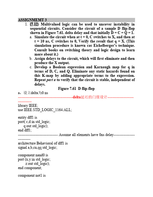
UX:未知不定 U1:未知1 U0:未知0 为了定义决断函数如何工作用了几个简单规定: 1、最强的强度总是赢家 2、强度相同而值不同,返回强度同但值为X 先比较强度: F R Z F F R Z
1、在Design_Vision中可以看到设计原理图如下,和ench对其进行测试
3、通过观察仿真波形可以看出,如下图所示,当C=1时,Q的状态和D 输入的状态是始终同步的。当C=X时,Q=X,在t=10ns时,C=0,而Q依 然保持Q=X。
b、设立delta为1 ns ,比较两者之间的区别 ------------------------------------------delta延迟的门级设计--------------------------------library IEEE; use IEEE.STD_LOGIC_1164.ALL; entity dff1 is port( c,d:in std_logic; q:out std_logic); end dff1; -------------------------------- Assume all elements have 3ns delay-------------------------architecture Behavioral of dff1 is signal a,b,cn,qq:std_logic;
D 0 0 1 1 0 0 1 1
Q 0 1 0 1 0 1 0 1
q 0 1 0 1 0 0 1 1
布尔逻辑表达式:q =QC’D’+C’DQ+CDQ’+CDQ 卡诺图: Q CD 00 01 11 0 0 0 1 1 1 1 1 化简可得到布尔逻辑表达式:q =QC’ +CD
哈工大cmos模拟集成电路大作业
H a r b i n I n s t i t u t e o f T e c h n o l o g y模拟C M O S集成电路大作业设计题目:二级运放设计院系:班级:设计者:学号:设计时间:2011.6.20哈尔滨工业大学2012年设计题:假定μn C ox=110 μA/V2,μp C ox=50 μA/V2,λn=0.04V-1,λp=0.04V-1(有效沟道长度为1μm时),λn=0.02V-1,λp=0.02V-1(有效沟道长度为2μm时),λn=0.01V-1,λp=0.01V-1(有效沟道长度为4μm时),γ=0.2,V THN=| V THP | =0.7V。
设计如下图的放大器,满足如下要求,其中负载电容C L= 10pF。
Av > 4000V/V,VDD = 5V,GB = 5MHz ,SR > 10V/µs ,60°相位裕度,Vout 摆幅=0.5~4.5V, ICMR 1.5~4.5V,Pdiss≤ 2mW1.请说明详细的设计过程,包括公式表达式(假定C ox = 0.35fF/µm2,栅源电容按计算);2.给出进行交流仿真和瞬态仿真的spice仿真的网表,并给出仿真波形和结果。
3.如果要求Av至少提高为原来的2倍,其它要求不变,如何修改电路(注意讨论对其它性能参数的影响)?注意事项:1.计算得到的极点频率为角频率。
2.尺寸最后应选取整数,工艺精度的限制。
3.尾电流增加,Av增加还是减小?1.根据相位裕度PM=60deg的要求,求C c(假定ωz>10GB);考虑零点的影响,CC的选取:PM=60°时,GB处︒-︒=⎪⎪⎭⎫ ⎝⎛+⎪⎪⎭⎫ ⎝⎛+⎪⎪⎭⎫ ⎝⎛60180c c c 21z p p GB tg ar GB tg ar GB tg ar ωωω令ωz =10GB 时()︒-︒=+⎪⎪⎭⎫⎝⎛+︒601801.0c c 902tg ar GB tg ar p ω若PM>60 °, ωp2>2.2GB ,并由ωz =10GB2.210mII mII L C g g C C >⨯由此可得:LC C C 22.0>负载电容C L =10pF,所以C c >2.2pF,取C c =3pF2.由已知的Cc 并根据转换速率的要求(或功耗要求)选择ISS (I5)的范围;A I A I s V S C I S r Cr μμμ40,30,/10555=>>=取可得,由3.由计算得到的电流偏置值(I5 /2),设计W3/L3( W4/L4 )满足上ICMR (或输出摆幅)要求,即饱和区条件;极限情况下,即ICMR 达最大4.5V 时,M3,M4管的过驱动电压为:3,4OD DD THn THpV V ICMR V V +=-+-由此可得,M3,M4管的漏电流:2253(4)3,411/2()2022p ox OD p ox DD THn THp W WI I C V C V ICMR V V A L L μμμ+===-+-=代入μp C ox =50 μA/V 2,VDD = 5V ,ICMR +=4.5V ,I 5=40μA ,V THN =| V THP | =0.7V 可得:3,43,4() 3.2()=4W WL L =,此时取4. 验证M3处镜像极点是否大于10GBGBC gC C g gs m gs gs m 10233433>=+验证F101.5008100.354440.6767.0-14-15333⨯=⨯⨯⨯⨯⨯==ox gs C L W CV A I L WC g oxp m /1044.891020410502266633---⨯=⨯⨯⨯⨯⨯=⋅=μ代入验证成立5. 设计W1/L1( W2/L2 )满足GB 的要求1/m cGB g C =6121110521032⨯⨯⨯⨯=⋅=⋅=-πμGB C I L WC g c oxn m由此解得:1,21,2()=2.01()=3W WL L ,此时取6. 设计W5/L5满足下ICMR (或输出摆幅)要求; 当ICMR 取最小值1.5V 时,M5管的过驱动电压为:-6151-61222010=1.5-0.7=0.45V (/)110103OD GS TH n ox I V ICMR V ICMR V C W L μ--⎛⎫⎛⎫⨯⨯=-=-++ ⎪ ⎪ ⎪ ⎪⨯⨯⎝⎭⎝⎭255)(21OD ox n V L W C I μ=4)(3.59)(55==L WL W ,取由此可得, 7. 根据ωp2>2.2GB 计算得到gm6;并且根据偏置条件VSG4=VSG6计算得到M6的尺寸6222GB=; 2.2C m m p p L Cg gGB C ωω=>由,且得: 62622.2/,=2.2/m m L c m m L cg g C C g g C C >令2266 2.2()()()()n ox GS THN L p ox GS THP cWC V V C WL C V V LC μμ--=所以2224421412;()()2422p ox GS THP n ox GS THN W W I I C V V C V V L L μμ=-=-根据电路结构得:即 64642(2/2),()(4/4)n GS GS GS THP GS THP GS THN p W L V V V V V V V V W L μμ=-=-=-又因为所以6666(W2/L2)(W4/L4)2.2 2.21011034:==37.68=38350n LC p W WC L C L μμ⨯⨯⨯=联立可得,取8. 根据尺寸和g m6计算I 6,并验证V out,max 是否满足要求666444/3820190/4W L I I AW L μ==⨯=66666221901060.45(/)501038OD p ox I M V V C W L μ--⨯⨯===⨯⨯管的过驱动电压:6,max 50.45 4.55,DD OD out V V V V -=-=>满足要求9. 计算M7的尺寸。
系统集成电路大作业

系统集成与应用实验设计报告16路模拟信号发生器班级:小组成员:指导教师:目录1、设计任务和要求分析 (2)2、整体方案设计选择 (2)3、理论计算 (6)4、电路设计及仿真 (7)5、实验总结 (11)六、附录 (12)一、设计任务与要求分析1.1设计任务用C8051F020单片机完成16路信号源的输出,并通过单片机内部A/D转换器进行输出信号源的反馈采样,最后通过异步串行接口(UART)将采样结果输出。
利用C8051单片机将波形量化数据放置于内部ROM,通过内部D/A产生信号以及I/O端口控制多路模拟开关,同时生成16路信号源,注意信号源调理电路中采保部分的选值,并给出理论计算结果。
反馈回采部分采用单片机的12位高精度A/D转换器,采样频率自定(要求给出理论计算值),并通过UART接口将采样值送出按9600bps的波特率发出(接收对象可以是计算机或其它)。
1.2任务要求分析我们通过集体讨论与分析,确定了如下的设计流程:图 1.系统流程图在进行具体的实验设计之后,我们进行了电路简化,放大滤波通过一个运算放大器来实现,不仅使电路得到了简化,而且也节省了资源。
二、整体方案设计选择2.1单片机部分单片机选用 C8051F020,是完全集成的混合信号系统级 MUC 芯片具有64个数字I/O引脚;具有12位100kps的8通道ADC,带PGA和多路模拟开关;具有2个12位DAC,具有可编程数据更新方式;64K可在系统编程的FLASH存储器;4352字节的片内RAM;可寻址64K字节地址空间的数据存储器接口:2个UART串行接口。
基于以上优良特性,故选用该单片机。
单片机具有上电复位、掉电复位、外部复位、软件强制复位等多种复位方式。
在应用中外部复位方式得到广泛应用。
外部/RST引脚提供使用外部电路使单片机强制复位的手段。
在外部/RST引脚加一个低电平有效信号,将使单片机复位,最好提供一个外部上拉,或对RST引脚去耦以防止噪声引起复位。
- 1、下载文档前请自行甄别文档内容的完整性,平台不提供额外的编辑、内容补充、找答案等附加服务。
- 2、"仅部分预览"的文档,不可在线预览部分如存在完整性等问题,可反馈申请退款(可完整预览的文档不适用该条件!)。
- 3、如文档侵犯您的权益,请联系客服反馈,我们会尽快为您处理(人工客服工作时间:9:00-18:30)。
实验一:
(1)分频:将八分频更改为二分频和四分频
在源程序中,将#0t_data_in=4'b0000;
#3000t_data_in=4'b1000;,分别改为#0t_data_in=4'b0000;
#3000t_data_in=4'b1100;和#0t_data_in=4'b0000;
#3000t_data_in=4'b1110;
即可得到四分频和二分频图像。
四
分
频
二分频
(2)反序:改变电路使彩灯变成逆时针旋转方式:
源程序改动
将源程序
4'b0000:lamp=16'b0000_0000_0000_0001;
4'b0001:lamp=16'b0000_0000_0000_0010;
4'b0010:lamp=16'b0000_0000_0000_0100;
4'b0011:lamp=16'b0000_0000_0000_1000;
4'b0100:lamp=16'b0000_0000_0001_0000;
4'b0101:lamp=16'b0000_0000_0010_0000;
4'b0110:lamp=16'b0000_0000_0100_0000;
4'b0111:lamp=16'b0000_0000_1000_0000;
4'b1000:lamp=16'b0000_0001_0000_0000;
4'b1001:lamp=16'b0000_0010_0000_0000;
4'b1010:lamp=16'b0000_0100_0000_0000;
4'b1011:lamp=16'b0000_1000_0000_0000;
4'b1100:lamp=16'b0001_0000_0000_0000;
4'b1101:lamp=16'b0010_0000_0000_0000;
4'b1110:lamp=16'b0100_0000_0000_0000;
4'b1111:lamp=16'b1000_0000_0000_0000;
default:lamp=16'b0000_0000_0000_0000;
首尾相对应语句依次调换位置,即可得到新的源程序,执行后可观测到新的亮灯顺序为反序。
(1)验证乘法器的正确性。
原始数据
更改输入数据,验证乘法器的正确性
(2)将乘法器改为8BITs
1.将源程序中
//data width definition
parameter mwidth=16;
parameter rwidth=mwidth+mwidth;
改为
//data width definition
parameter mwidth=8;
parameter rwidth=mwidth+mwidth;
2.reg[3:0]mucnt;
//multiplicand register
改为reg[2:0]mucnt;
//multiplicand register
3
//multiply process end
assign mucnt_full=(mucnt==4'b1111)?1'b1:1'b0;改为
//multiply process end
assign mucnt_full=(mucnt==3'b111)?1'b1:1'b0;
4.begin
if(rst)
mucnt<=4'b0000;
else if(mucnt_en)
mucnt<=mucnt+1;
改为begin
if(rst)
mucnt<=3'b000;
else if(mucnt_en)
mucnt<=mucnt+1;
5.reg rst,clk;
reg[15:0]x,y;
wire[31:0]result;
改为reg rst,clk;
reg[7:0]x,y;
wire[15:0]result;
6.x=16'h0000;
y=16'h0003;
#25rst=1'b0;
#160x=16'h0012;
y=16'h0013;
#160x=16'h0134;
y=16'h0213;
#160x=16'h1234;
y=16'h2587;
#160x=16'hffff;
y=16'hffff;
改为x=16'h00;
y=16'h03;
#25rst=1'b0;
#160x=16'h12;
y=16'h13;
#160x=16'h34;
y=16'h13;
#160x=16'h34;
y=16'h87;
#160x=16'hff;
y=16'hff;
最终得到图像
8bits。