驱动芯片BTS7970B介绍
中国联通上海贝尔BTS维护操作手册

中国联通上海贝尔BTS维护操作手册1.0版本2010.04目录1系统结构及重要硬件介绍 (4)1.1前言 (4)1.2BTS的功能块介绍 (5)1.2.1BTS的体系 (5)1.2.2电信功能 (8)1.2.3操作和维护的功能 (9)1.2.4传输功能 (10)1.2.5天馈网络 (11)1.3BTS硬件硬件板卡介绍 (12)1.3.1概述 (12)1.3.2SUM 板 (16)1.3.3收发信机(TRE) (21)1.3.4天线网络 (31)1.3.5BTS 的外部连接 (46)1.3.6风扇单元 (48)1.3.7BTS机架 (49)2维护作业计划操作指导 (49)2.1维护作业计划概述 (49)2.2维护作业计划内容 (49)2.2.1日常维护项目 (49)2.2.2周度维护项目 (50)2.2.3月度维护项目 (50)2.2.4年度维护项目 (51)3BTS重要操作维护指导 (51)3.19110-E Micro BTS维护 (51)3.1.1BTS终端概述 (51)3.1.2BTS终端的连接 (52)3.1.3启动BTS终端 (52)3.2安全块的定义和处理 (57)3.2.1SBL 的定义 (57)3.2.2SBL 状态 (59)3.2.3SBL 状态 (59)3.2.4SBL 操作命令 (62)3.2.5SBL 与RIT之间的关系 (64)3.2.6设置TMA采用菜单: (66)3.3更新内部数据(RI) (67)3.3.1读取RI (67)3.3.2修改RI (67)3.4传输设置 (68)3.4.1使用Setting 菜单 (68)3.4.2设置Qmux 地址 (68)3.4.3检查告警表 (69)3.4.4确认Qmux 状态 (69)3.4.5环路调试 (70)3.4.6设置时钟模式 (70)3.4.7设置并检查Abis映射表 (71)4常用软硬件工具介绍 (72)5常见故障处理 (72)1系统结构及重要硬件介绍1.1前言基站收发信台(BTS)是基站子系统(BSS)的无线部分。
电赛论文模板
2015年全国大学生电子设计竞赛简易旋转倒立摆及控制装置(C题)【本科组】2013年9月6日目录1系统方案 (2)1.1电机及驱动方案的论证与选择 (2)1.2传感器采集模块的论证与选择 (2)1.3 控制系统的论证与选择 (2)2系统理论分析与计算 (3)2.1 XXXX的分析 (3)2.1.1 XXX (3)2.1.2 XXX (3)2.1.3 XXX (3)2.2 XXXX的计算 (3)2.2.1 XXX (3)2.2.2 XXX (3)2.2.3 XXX (3)2.3 XXXX的计算 (3)2.3.1 XXX (3)2.3.2 XXX (3)2.3.3 XXX (3)3电路与程序设计 (3)3.1电路的设计 (3)3.1.1系统总体框图 (3)3.1.2 XXXX子系统框图与电路原理图 (4)3.1.3 XXXX子系统框图与电路原理图 (4)3.1.4电源 (4)3.2程序的设计 (4)3.2.1程序功能描述与设计思路 (4)3.2.2程序流程图 (5)4测试方案与测试结果 (5)4.1测试方案 (5)4.2 测试条件与仪器 (5)4.3 测试结果及分析 (6)4.3.1测试结果(数据) (6)4.3.2测试分析与结论 (6)附录1:电路原理图 (7)附录2:源程序 (8)简易旋转倒立摆及控制装置(C题)【本科组】1系统方案本系统主要由电机及驱动模块、传感器采集模块、控制器模块、电源模块组成,下面分别论证这几个模块的选择。
1.1电机及驱动方案的论证与选择方案一:42BY系列混合式步进电机+LN298驱动方案此方案在最先想到以及调试的方案,用步进电机的有点就是正反转切换迅速,无堵转现象,转矩大,负载能力强。
但是42BY系列混合式步进电机响应一拍最小周期为2ms,此时处于电机为最大转速,执行周期长,也就造成系统控制周期长,但是本系统要求调节周期短(我们最终方案采用的是2ms),能够在极短时间内实现一个调节过程,故此方案不能达到预期的效果。
BTS7970

t h i n k i n g .BTS 7970BHigh Current PN Half Bridge NovalithIC68A, 7m Ω + 9m Ω typ.TM查询BTS7970B供应商High Current PN Half BridgeBTS 7970BData Sheet 1Rev. 2.0, 2006-05-09Product Summary . . . . . . . . . . . . . . . . . . . . . . . . . . . . . . . . . . . . . . . . . . . . . . . . . . . .2Basic Features . . . . . . . . . . . . . . . . . . . . . . . . . . . . . . . . . . . . . . . . . . . . . . . . . . . . . . .21Overview . . . . . . . . . . . . . . . . . . . . . . . . . . . . . . . . . . . . . . . . . . . . . . . . . . . . . . . . .31.1Block Diagram . . . . . . . . . . . . . . . . . . . . . . . . . . . . . . . . . . . . . . . . . . . . . . . . . . .31.2Terms . . . . . . . . . . . . . . . . . . . . . . . . . . . . . . . . . . . . . . . . . . . . . . . . . . . . . . . . .42Pin Configuration . . . . . . . . . . . . . . . . . . . . . . . . . . . . . . . . . . . . . . . . . . . . . . . . . .52.1Pin Assignment . . . . . . . . . . . . . . . . . . . . . . . . . . . . . . . . . . . . . . . . . . . . . . . . . .52.2Pin Definitions and Functions . . . . . . . . . . . . . . . . . . . . . . . . . . . . . . . . . . . . . . .53Maximum Ratings . . . . . . . . . . . . . . . . . . . . . . . . . . . . . . . . . . . . . . . . . . . . . . . . . .6Maximum Single Pulse Current . . . . . . . . . . . . . . . . . . . . . . . . . . . . . . . . . . . . . . . . .71Block Description and Characteristics . . . . . . . . . . . . . . . . . . . . . . . . . . . . . . . . .81.1Supply Characteristics . . . . . . . . . . . . . . . . . . . . . . . . . . . . . . . . . . . . . . . . . . . . .81.2Power Stages . . . . . . . . . . . . . . . . . . . . . . . . . . . . . . . . . . . . . . . . . . . . . . . . . . .91.2.1Power Stages - Static Characteristics . . . . . . . . . . . . . . . . . . . . . . . . . . . 101.2.2Switching Times . . . . . . . . . . . . . . . . . . . . . . . . . . . . . . . . . . . . . . . . . . . 111.2.3Power Stages - Dynamic Characteristics . . . . . . . . . . . . . . . . . . . . . . . . 121.3Protection Functions . . . . . . . . . . . . . . . . . . . . . . . . . . . . . . . . . . . . . . . . . . . . .141.3.1Overvoltage Lock Out . . . . . . . . . . . . . . . . . . . . . . . . . . . . . . . . . . . . . . . 141.3.2Undervoltage Shut Down . . . . . . . . . . . . . . . . . . . . . . . . . . . . . . . . . . . . . 141.3.3Overtemperature Protection . . . . . . . . . . . . . . . . . . . . . . . . . . . . . . . . . . 141.3.4Current Limitation . . . . . . . . . . . . . . . . . . . . . . . . . . . . . . . . . . . . . . . . . . 141.3.5Short Circuit Protection . . . . . . . . . . . . . . . . . . . . . . . . . . . . . . . . . . . . . . 161.3.6Electrical Characteristics - Protection Functions . . . . . . . . . . . . . . . . . . . 171.4Control and Diagnostics . . . . . . . . . . . . . . . . . . . . . . . . . . . . . . . . . . . . . . . . . .181.4.1Input Circuit . . . . . . . . . . . . . . . . . . . . . . . . . . . . . . . . . . . . . . . . . . . . . . . 181.4.2Dead Time Generation . . . . . . . . . . . . . . . . . . . . . . . . . . . . . . . . . . . . . . 181.4.3Adjustable Slew Rate . . . . . . . . . . . . . . . . . . . . . . . . . . . . . . . . . . . . . . . 181.4.4Status Flag Diagnosis With Current Sense Capability . . . . . . . . . . . . . . 181.4.5Truth Table . . . . . . . . . . . . . . . . . . . . . . . . . . . . . . . . . . . . . . . . . . . . . . . 201.4.6Electrical Characteristics - Control and Diagnostics . . . . . . . . . . . . . . . . 212Thermal Characteristics . . . . . . . . . . . . . . . . . . . . . . . . . . . . . . . . . . . . . . . . . . . .223Application . . . . . . . . . . . . . . . . . . . . . . . . . . . . . . . . . . . . . . . . . . . . . . . . . . . . . . .233.1Application Example . . . . . . . . . . . . . . . . . . . . . . . . . . . . . . . . . . . . . . . . . . . . .233.2Layout Considerations . . . . . . . . . . . . . . . . . . . . . . . . . . . . . . . . . . . . . . . . . . . .234Package Outlines P-TO-263-7 . . . . . . . . . . . . . . . . . . . . . . . . . . . . . . . . . . . . . . .245Revision History . . . . . . . . . . . . . . . . . . . . . . . . . . . . . . . . . . . . . . . . . . . . . . . . . .25Data Sheet2Rev. 2.0, 2006-05-09Type Package BTS7970BP-TO-263-7High Current PN Half Bridge NovalithIC BTS 7970BProduct SummaryThe BTS 7970B is a fully integrated high current halfbridge for motor drive applications. It is part of theNovalithIC TM family containing one p-channel highside MOSFET and one n-channel lowside MOSFET with an integrated driver IC in one package. Due to the p-channel highside switch the need for a charge pump is eliminated thus minimizing EMI. Interfacing to a microcontroller is made easy by the integrated driver IC which features logic level inputs, diagnosis with current sense, slew rateadjustment, dead time generation and protection against overtemperature, overvoltage,undervoltage, overcurrent and short circuit.The BTS 7970B provides a cost optimized solution for protected high current PWM motor drives with very low board space consumption.Basic Features•Path resistance of typ. 16m Ω@25°C •Low quiescent current of typ. 7µA @25°C•PWM capability of up to 25kHz combined with active freewheeling•Switched mode current limitation for reduced power dissipation in overcurrent •Current limitation level of 68A typ. / 50A min.•Status flag diagnosis with current sense capability •Overtemperature shut down with latch behaviour•Overvoltage lock out •Undervoltage shut down•Driver circuit with logic level inputs•Adjustable slew rates for optimized EMIBTS 7970BP-TO-263-7TMHigh Current PN Half BridgeBTS 7970BOverviewData Sheet 3Rev. 2.0, 2006-05-091OverviewThe BTS 7970B is part of the NovalithIC family containing three separate chips in one package: One p-channel highside MOSFET and one n-channel lowside MOSFET together with a driver IC, forming a fully integrated high current half-bridge. All three chips are mounted on one common leadframe, using the chip on chip and chip by chip technology. The power switches utilize vertical MOS technologies to ensure optimum on state resistance. Due to the p-channel highside switch the need for a charge pump is eliminated thus minimizing EMI. Interfacing to a microcontroller is made easy by the integrated driver IC which features logic level inputs, diagnosis with current sense, slew rate adjustment, dead time generation and protection against overtemperature,overvoltage, undervoltage, overcurrent and short circuit. The BTS 7970B can be combined with other BTS 7970B to form H-bridge and 3-phase drive configurations.1.1Block DiagramFigure 1Block DiagramHigh Current PN Half BridgeBTS 7970BOverviewData Sheet 4Rev. 2.0, 2006-05-091.2TermsFollowing figure shows the terms used in this data sheet.Figure 2TermsHigh Current PN Half BridgeBTS 7970BPin ConfigurationData Sheet5Rev. 2.0, 2006-05-092Pin Configuration2.1Pin AssignmentFigure 3Pin Assignment BTS 7970B and (top view)2.2Pin Definitions and FunctionsBold type: Pin needs power wiringPin Symbol I/O Function 1GND -Ground2IN I InputDefines whether high- or lowside switch is activated 3INH I InhibitWhen set to low device goes in sleep mode 4,8OUT OPower output of the bridge5SRISlew RateThe slew rate of the power switches can be adjusted by connecting a resistor between SR and GND 6IS O Current Sense and Diagnosis 7VS-SupplyHigh Current PN Half BridgeBTS 7970BMaximum RatingsData Sheet 6Rev. 2.0, 2006-05-093Maximum RatingsNote:Maximum ratings are absolute ratings; exceeding any one of these values maycause irreversible damage to the device. Exposure to maximum rating conditions for extended periods of time may affect device reliability-40 °C < T j < 150°C (unless otherwise specified)PosParameterSymbolLimits UnitTest Conditionminmax Electrical Maximum Ratings 3.0.1Supply voltage V VS-0.345V 3.0.2Logic Input Voltage V INV INH-0.3 5.3V 3.0.3HS/LS continuous drain currentI D(HS)I D(LS)-44441)1)Maximum reachable current may be smaller depending on current limitation level A T C < 85°C switch active3.0.4HS pulsed drain current I D(HS)-90901)A T C < 85°Ct pulse = 10ms single pulse 3.0.5LS pulsed drain current I D(LS)-90901)A 3.0.6PWM current I OUT 1)-5555A f = 1kHz, DC = 50%-6060A f = 20kHz, DC = 50%3.0.7Voltage at SR pin V SR -0.31.0V 3.0.8Voltage between VS and IS pinV VS -V IS -0.345V 3.0.9Voltage at IS pinV IS -2045V Thermal Maximum Ratings 3.0.10Junction temperature T j -40150°C 3.0.11Storage temperature T stg -55150°C ESD Susceptibility 3.0.12ESD susceptibilityIN, INH, SR, IS OUT, GND, VSV ESD-2-626kVHBM 2)2)ESD susceptibility HBM according to EIA/JESD 22-A 114BHigh Current PN Half BridgeBTS 7970BMaximum RatingsData Sheet 7Rev. 2.0, 2006-05-09Maximum Single Pulse CurrentFigure 4BTS 7970B Maximum Single Pulse CurrentThis diagram shows the maximum single pulse current that can be driven for a given pulse time t pulse . The maximum reachable current may be smaller depending on the current limitation level. Pulse time may be limited due to thermal protection of the device.High Current PN Half BridgeBTS 7970BBlock Description and CharacteristicsData Sheet8Rev. 2.0, 2006-05-094Block Description and Characteristics4.1Supply CharacteristicsFigure 5Quiescent Current (typ.) vs. Junction Temperature– 40 °C < T j < 150 °C, 8 V < V S < 18 V, I L = 0A (unless otherwise specified)Pos.Parameter Symbol Limit Values Unit Test Conditionsmin.typ.max.General 4.1.1Operating Voltage V S5.5–28V V S increasing 4.1.2Supply CurrentI VS(on)–23mAV INH = 5VV IN = 0V or 5V R SR =0ΩDC-modenormal operation (no fault condition)4.1.3Quiescent CurrentI VS(off)–715µAV INH = 0VV IN = 0V or 5V T j <85°C ––65µAV INH = 0VV IN = 0V or 5VHigh Current PN Half BridgeBTS 7970BBlock Description and CharacteristicsData Sheet 9Rev. 2.0, 2006-05-094.2Power StagesThe power stages of the BTS 7970B consist of a p-channel vertical DMOS transistor for the high side switch and a n-channel vertical DMOS transistor for the low side switch. All protection and diagnostic functions are located in a separate top chip. Both switches can be operated up to 25 kHz, allowing active freewheeling and thus minimizing power dissipation in the forward operation of the integrated diodes.The on state resistance R ON is dependent on the supply voltage V S as well as on the junction temperature T j . The typical on state resistance characteristics are shown in Figure 6.Figure 6Typical On State Resistance vs. Supply VoltageHigh Current PN Half BridgeBTS 7970BBlock Description and CharacteristicsData Sheet 10Rev. 2.0, 2006-05-094.2.1Power Stages - Static Characteristics– 40 °C < T j < 150 °C, 8 V < V S < 18 V (unless otherwise specified)Pos.Parameter Symbol Limit Values Unit Test Conditionsmin.typ.max.High Side Switch - Static Characteristics 4.2.1On state high sideresistanceR ON(HS)––710912.5m ΩI OUT = 20A V S = 13.5V T j = 25°C T j = 150°C 4.2.2Leakage current high sideI L(LKHS)––1µAV INH = 0V V OUT = 0V T j < 85 °C ––50µAV INH = 0V V OUT = 0 V T j = 150 °C 4.2.3Reverse diodeforward-voltage high side 1)1)Due to active freewheeling, diode is conducting only for a few µs, depending on R SRV DS(HS)–––0.90.80.61.51.10.8VI OUT =-9A T j = -40 °C T j = 25 °C T j = 150 °C Low Side Switch - Static Characteristics 4.2.4On state low side resistanceR ON(LS)––9141218m ΩI OUT =-20A V S = 13.5V T j = 25 °C T j = 150 °C 4.2.5Leakage current low sideI L(LKLS)––1µAV INH = 0V V OUT = V S T j < 85 °C ––15µAV INH = 0V V OUT = V S T j = 150 °C 4.2.6Reverse diodeforward-voltage low side 1)V SD(LS)–––0.90.80.61.51.10.8VI OUT = 9A T j = -40 °C T j = 25 °C T j = 150 °CHigh Current PN Half BridgeBTS 7970BBlock Description and CharacteristicsData Sheet 11Rev. 2.0, 2006-05-094.2.2Switching TimesFigure 7Definition of switching times high side (R load to GND)Figure 8Definition of switching times low side (R load to VS)Due to the timing differences for the rising and the falling edge there will be a slight difference between the length of the input pulse and the length of the output pulse. It can be calculated using the following formulas:•∆t HS = (t dr(HS) + 0.5 t r(HS)) - (t df(HS) + 0.5 t f(HS))•∆t LS = (t df(LS) + 0.5 t f(LS)) - (t dr(LS) + 0.5 t r(LS)).High Current PN Half BridgeBTS 7970BBlock Description and CharacteristicsData Sheet 12Rev. 2.0, 2006-05-094.2.3Power Stages - Dynamic Characteristics-40 °C < T j < 150 °C, V S = 13.5 V, R load = 2Ω (unless otherwise specified)Pos.Parameter Symbol Limit Values Unit Test Conditionsmin.typ.max.HIgh Side Switch Dynamic Characteristics 4.2.7Rise-time of HSt r(HS)0.5–2126 1.5–11µsR SR = 0ΩR SR = 5.1k ΩR SR = 51k Ω4.2.8Slew rate HS on∆V OUT /t r( HS)–––1161.6–––V/µs R SR = 0ΩR SR = 5.1k ΩR SR = 51k Ω4.2.9Switch on delay time HSt dr(HS)1.7–5.6 3.14.414 4.3–22.4µs R SR = 0ΩR SR = 5.1k ΩR SR = 51k Ω4.2.10Fall-time of HSt f(HS)0.5–2126 1.5–11µs R SR = 0ΩR SR = 5.1k ΩR SR = 51k Ω4.2.11Slew rate HS off-∆V OUT /t f(HS)–––1161.6–––V/µs R SR = 0ΩR SR = 5.1k ΩR SR = 51k Ω4.2.12Switch off delay timeHSt df(HS)1.2–42.43.4103.2–16µs R SR = 0ΩR SR = 5.1k ΩR SR = 51k ΩHigh Current PN Half BridgeBTS 7970BBlock Description and CharacteristicsData Sheet 13Rev. 2.0, 2006-05-09Low Side Switch Dynamic Characteristics 4.2.13Rise-time of LSt r(LS)0.5–2126 1.5–11µsR SR = 0ΩR SR = 5.1k ΩR SR = 51k Ω4.2.14Slew rate LS switch off ∆V OUT /t r(LS)–––1161.6–––V/µs R SR = 0ΩR SR = 5.1k ΩR SR = 51k Ω4.2.15Switch off delay timeLSt dr(LS)0.6–2.6 1.32.27 1.9–11µs R SR = 0ΩR SR = 5.1k ΩR SR = 51k Ω4.2.16Fall-time of LSt f(LS)0.5–2126 1.5–11µs R SR = 0ΩR SR = 5.1k ΩR SR = 51k Ω4.2.17Slew rate LS switch on -∆V OUT /t f(LS)–––1161.6–––V/µs R SR = 0ΩR SR = 5.1k ΩR SR = 51k Ω4.2.18Switch on delay timeLSt df(LS)2.3–6.43.65.6165.0–25.4µs R SR = 0ΩR SR = 5.1k ΩR SR = 51k Ω-40 °C < T j < 150 °C, V S = 13.5 V, R load = 2Ω (unless otherwise specified)Pos.Parameter Symbol Limit Values Unit Test Conditionsmin.typ.max.High Current PN Half BridgeBTS 7970BBlock Description and CharacteristicsData Sheet14Rev. 2.0, 2006-05-094.3Protection FunctionsThe device provides integrated protection functions. These are designed to prevent IC destruction under fault conditions described in the data sheet. Fault conditions are considered as “outside” normal operating range. Protection functions are not to be used for continuous or repetitive operation, with the exception of the current limitation (Chapter 4.3.4). In a fault condition the BTS 7970B will apply the highest slew rate possible independent of the connected slew rate resistor. Overvoltage, overtemperature and overcurrent are indicated by a fault current I IS(LIM) at the IS pin as described in the paragraph “Status Flag Diagnosis With Current Sense Capability” on Page 18 and Figure 12.In the following the protection functions are listed in order of their priority. Overvoltage lock out overrides all other error modes.4.3.1Overvoltage Lock OutTo assure a high immunity against overvoltages (e.g. load dump conditions) the device shuts the lowside MOSFET off and turns the highside MOSFET on, if the supply voltage is exceeding the over voltage protection level V OV(OFF). The IC operates in normal mode again with a hysteresis V OV(HY) if the supply voltage decreases below the switch-on voltage V OV(ON). In H-bridge configuration, this behavior of the BTS 7970B will lead to freewheeling in highside during over voltage.4.3.2Undervoltage Shut DownTo avoid uncontrolled motion of the driven motor at low voltages the device shuts off (output is tri-state), if the supply voltage drops below the switch-off voltage V UV(OFF). The IC becomes active again with a hysteresis V UV(HY) if the supply voltage rises above the switch-on voltage V UV(ON).4.3.3Overtemperature ProtectionThe BTS 7970B is protected against overtemperature by an integrated temperature sensor. Overtemperature leads to a shut down of both output stages. This state is latched until the device is reset by a low signal with a minimum length of t reset at the INH pin, provided that its temperature has decreased at least the thermal hysteresis ∆T in the meantime.Repetitive use of the overtemperature protection might reduce lifetime.4.3.4Current LimitationThe current in the bridge is measured in both switches. As soon as the current in forward direction in one switch (high side or low side) is reaching the limit I CLx , this switch is deactivated and the other switch is activated for t CLS . During that time all changes at theHigh Current PN Half BridgeBTS 7970BBlock Description and CharacteristicsData Sheet15Rev. 2.0, 2006-05-09IN pin are ignored. However, the INH pin can still be used to switch both MOSFETs off.After t CLS the switches return to their initial setting. The error signal at the IS pin is reset after 2 * t CLS . Unintentional triggering of the current limitation by short current spikes (e.g. inflicted by EMI coming from the motor) is suppressed by internal filter circuitry. Due to thresholds and reaction delay times of the filter circuitry the effective current limitation level I CLx depends on the slew rate of the load current d I /d t as shown in Figure 10Figure 9Timing Diagram Current Limitation (Inductive Load)Figure 10Current Limitation Level vs. Current Slew Rate dI/dtHigh Current PN Half BridgeBTS 7970BBlock Description and CharacteristicsData Sheet 16Rev. 2.0, 2006-05-09Figure 11Typical Current Limitation Detection Levels vs. Supply VoltageIn combination with a typical inductive load, such as a motor, this results in a switched mode current limitation. That way of limiting the current has the advantage that the power dissipation in the BTS 7970B is much smaller than by driving the MOSFETs in linear mode. Therefore it is possible to use the current limitation for a short time without exceeding the maximum allowed junction temperature (e.g. for limiting the inrush current during motor start up). However, the regular use of the current limitation is allowed only as long as the specified maximum junction temperature is not exceeded. Exceeding this temperature can reduce the lifetime of the device.4.3.5Short Circuit ProtectionThe device is short circuit protected against •output short circuit to ground•output short circuit to supply voltage •short circuit of loadThe short circuit protection is realized by the previously described current limitation in combination with the over-temperature shut down of the device.Please note: Due to the higher priority of the overvoltage protection the short circuit protection is inactive in overvoltage conditions.High Current PN Half BridgeBTS 7970BBlock Description and CharacteristicsData Sheet 17Rev. 2.0, 2006-05-094.3.6Electrical Characteristics - Protection Functions– 40 °C < T j < 150 °C; 8 V < V S < 18 V (unless otherwise specified)Pos.Parameter Symbol Limit Values Unit Test Conditionsmin.typ.max.Under Voltage Shut Down 4.3.1Switch-ON voltage V UV(ON)–– 5.5V V S increasing 4.3.2Switch-OFF voltage V UV(OFF) 4.0– 5.4V V S decreasing4.3.3ON/OFF hysteresis V UV(HY)–0.2–V –Over Voltage Lock Out4.3.4Switch-ON voltage V OV(ON)27.8––V V S decreasing4.3.5Switch-OFF voltage V OV(OFF)28–30V V S increasing4.3.6ON/OFF hysteresis V OV(HY)–0.2–V –Current Limitation4.3.7Current limitationdetection level high sideI CLH054–5076737098–90AV S =13.5V T j = -40 °C T j = 25 °C T j = 150 °C 4.3.8Current limitation detection level low sideI CLL054–5071686590–82A V S =13.5V T j = -40 °C T j = 25 °C T j = 150 °C Current Limitation Timing 4.3.9Shut off time for HS and LSt CLS70115210µsV S =13.5VThermal Shut Down 4.3.10Thermal shut downjunction temperature T jSD 155175200°C –4.3.11Thermal switch onjunction temperature T jSO150–190°C –4.3.12Thermal hysteresis∆T–7–K –4.3.13Reset pulse at INH pin (INH low)t reset4––µs–High Current PN Half BridgeBTS 7970BBlock Description and CharacteristicsData Sheet18Rev. 2.0, 2006-05-094.4Control and Diagnostics 4.4.1Input CircuitThe control inputs IN and INH consist of TTL/CMOS compatible schmitt triggers with hysteresis which control the integrated gate drivers for the MOSFETs. Setting the INH pin to high enables the device. In this condition one of the two power switches is switched on depending on the status of the IN pin. To deactivate both switches, the INH pin has to be set to low. No external driver is needed. The BTS 7970B can be interfaced directly to a microcontroller.4.4.2Dead Time GenerationIn bridge applications it has to be assured that the highside and lowside MOSFET are not conducting at the same time, connecting directly the battery voltage to GND. This is assured by a circuit in the driver IC, generating a so called dead time between switching off one MOSFET and switching on the other. The dead time generated in the driver IC is automatically adjusted to the selected slew rate.4.4.3Adjustable Slew RateIn order to optimize electromagnetic emission, the switching speed of the MOSFETs is adjustable by an external resistor. The slew rate pin SR allows the user to optimize the balance between emission and power dissipation within his own application by connecting an external resistor R SR to GND.4.4.4Status Flag Diagnosis With Current Sense CapabilityThe status pin IS is used as a combined current sense and error flag output. In normal operation (current sense mode), a current source is connected to the status pin, which delivers a current proportional to the forward load current flowing through the active high side switch. If the high side switch is inactive or the current is flowing in the reverse direction no current will be driven except for a marginal leakage current I IS(LK). The external resistor R IS determines the voltage per output current. E.g. with the nominal value of 19500 for the current sense ratio k ILIS = I L / I IS , a resistor value of R IS = 1k Ωleads to V IS = (I L / 19.5 A )V.Due to the good long term stability and the low temperature coefficient it is possible to improve the absolute current sense accuracy in the application by calibration. For best results it is recommended to do a two-point calibration.In case of a fault condition the status output is connected to a current source which is independent of the load current and provides I IS(lim). The maximum voltage at the IS pin is determined by the choice of the external resistor and the supply voltage. In case of current limitation the I IS(lim) is activated for 2 * t CLS .High Current PN Half BridgeBTS 7970BBlock Description and CharacteristicsData Sheet 19Rev. 2.0, 2006-05-09Figure 12Sense Current and Fault CurrentFigure 13Sense Current vs. Load CurrentHigh Current PN Half BridgeBTS 7970BBlock Description and CharacteristicsData Sheet 20Rev. 2.0, 2006-05-094.4.5Truth TableDevice State Inputs Outputs ModeINHIN HSS LSS IS Normal operation0X OFF OFF 0Stand-by mode 10OFF ON 0LSS active 11ON OFF CS HSS active Over-voltage (OV)XXONOFF1Shut-down of LSS,HSS activated, error detected Under-voltage (UV)X X OFF OFF 0UV lockoutOvertemperature (OT)0X OFF OFF 0Stand-by mode, reset of latch1X OFF OFF 1Shut-down with latch, error detected Current limitation 11OFF ON 1Switched mode, error detected 1)1)Will return to normal operation after t CLS ; Error signal is reset after 2*t CLS (see Chapter 4.3.4)1ONOFF1Switched mode , error detected 1)Inputs:Switches Status Flag IS:0 = Logic LOW OFF = switched off CS = Current sense mode 1 = Logic HIGH ON = switched on1 = Logic HIGH (error)X = 0 or 1High Current PN Half BridgeBTS 7970BBlock Description and CharacteristicsData Sheet 21Rev. 2.0, 2006-05-094.4.6Electrical Characteristics - Control and Diagnostics– 40 °C < T j < 150 °C, 8 V < V S < 18 V (unless otherwise specified)Pos.Parameter Symbol Limit Values Unit Test Conditionsmin.typ.max.Control Inputs (IN and INH)4.4.1High level voltageINH, INV INH(H) V IN(H)– 1.751.6 2.152V –4.4.2Low level voltage INH, IN V INH(L) V IN(L) 1.1 1.4–V –4.4.3Input voltage hysteresis V INHHY V INHY ––350200––mV–4.4.4Input current I INH(H)I IN(H)–30150µA V IN = V INH =5.3 V 4.4.5Input currentI INH(L)I IN(L)–25125µAV IN = V INH =0.4 VCurrent Sense 4.4.6Current sense ratio in static on-condition k ILIS = I L / I ISk ILIS 13121019.519.519.5252628103R IS = 1 k ΩI L = 40A I L = 20A I L = 10A 4.4.7Maximum analog sense current, sense current in fault conditionI IS(lim)456.5mA V S = 13.5 VR IS = 1k Ω4.4.8Isense leakage current I ISL ––1µA V IN = 0V or V INH = 0V4.4.9Isense leakage current,active high side switchI ISH –1200µA V IN = V INH = 5V I L = 0A4.4.10Current sense ratiolong term drift 1)1)Not subject to production test, specified by design.dk ILIS -1.51.5%Q100 qualification4.4.11Current sense ratio temperaturecoefficient 1)dk ILIS /dT-0.12-0.0250.06%/K I L = 10A4.4.12-0.055-0.0250.005I L = 20A4.4.13-0.05-0.0250I L = 40AHigh Current PN Half BridgeBTS 7970BThermal CharacteristicsData Sheet 22Rev. 2.0, 2006-05-095Thermal CharacteristicsNote:Thermal characteristics are not subject to production test - specified by design.PosParameterSymbolLimits Unit Test Condition min max 5.0.1Thermal Resistance Junction-Case, Low Side Switch R thjc(LS) = ∆T j(LS)/ P v(LS)R thjc(LS)–1.8K/W5.0.2Thermal Resistance Junction-Case, High Side Switch R thjc(HS) = ∆T j(HS)/ P v(HS)R thjc(HS)–0.9K/W5.0.3Thermal ResistanceJunction-Case, both Switches R thjc = max[∆T j(HS), ∆T j(LS)] /(P v(HS) + P v(LS))R thjc– 1.0K/W5.0.4Thermal ResistanceJunction-AmbientR thja–35K/W 6cm 2 coolingareaHigh Current PN Half BridgeBTS 7970BApplicationData Sheet23Rev. 2.0, 2006-05-096ApplicationFigure 14Application Example: H-Bridge with two BTS 7970B6.2Layout ConsiderationsDue to the fast switching times for high currents, special care has to be taken to the PCB layout. Stray inductances have to be minimized in the power bridge design as it is necessary in all switched high power bridges. The BTS 7970B has no separate pin for power ground and logic ground. Therefore it is recommended to assure that the offset between the ground connection of the slew rate resistor, the current sense resistor and ground pin of the device (GND / pin 1) is minimized. If the BTS 7970B is used in a H-bridge or B6 bridge design, the voltage offset between the GND pins of the different devices should be small as well.A ceramic capacitor from VS to GND close to each device is recommended to provide current for the switching phase via a low inductance path and therefore reducing noise and ground bounce. A reasonable value for this capacitor would be about 470 nF.The digital inputs need to be protected from excess currents (e.g. caused by induced voltage spikes) by series resistors in the range of 10 k Ω.。
BTS7970-BTS7960及其他直流电机驱动模块

BTS7970-BTS7960及其他直流电机驱动模块在机械设备中,电机的作用非常重要,而它们的使用涉及到很多细节,其中就包括电机驱动模块。
直流电机驱动模块的作用就是将控制信号转换为电动机信号,从而使电动机正常工作。
本文将介绍其中的一些常见型号,包括BTS7970和BTS7960。
什么是BTS7970?BTS7970是一种直流电机驱动模块,由Infineon公司生产。
它的主要特点包括:•可以承受最大43A输出电流•能够在高达60V的电压下工作•具有低内部阻抗•内置过热保护和过电流保护功能这款模块通常被用于电动汽车、无人机和机器人等需要高功率的应用。
值得注意的是,BTS7970模块需要配合外部控制器使用,以便能够正确驱动电机。
什么是BTS7960?BTS7960也是一种直流电机驱动模块,同样由Infineon公司生产。
相比BTS7970,它的最大输出电流稍小,只有40A,并且在高压(30V至57V)应用下工作。
另外,BTS7960也具有高效的功能如短路保护、过热保护以及过电流保护,以确保设备的安全性。
如何选择正确的直流电机驱动模块?选择直流电机驱动模块时,需要考虑一系列因素。
确认电机参数电机的参数,如电流、电压、功率,都会影响模块的选择。
不同电机需要不同电流输出,因此需要为电机选择与其匹配的模块。
确认电机与控制器的接口除了电机的参数外,还需要考虑控制器与驱动器之间的接口是否兼容。
这将涉及到电机的控制方式,如PWM(脉冲宽度调制)、模拟信号控制或串行通信控制。
控制器与驱动模块之间的接口必须匹配,否则电机将无法正常工作。
确认被驱动的负载最后,需要确定被驱动的负载类型,如风扇、泵、飞行器或车辆。
这是因为不同的负载具有不同的动态特性,而电机驱动模块的选型也会受到这些因素的影响。
直流电机驱动模块的应用直流电机驱动模块广泛应用于自动化设备、电动车、轨道交通、船舶、机器人等方面。
以下是一些直流电机驱动模块的常见应用场景:电动车在电动车中,直流电机驱动模块做为中间设备,将电池组的直流电能转换为电机的转动动能。
常用电机驱动电路及原理
EN1 和 EN2 一般使用时我们直接接高电平,使整个电路始终处于工作状态!
通过对上面电路的了解,大家应该大致了解了 H 桥的基本工作原理,有没有更 好地驱动电路了呢?答案是肯定的!以下是直流电动机的机械特性表达式:
n 是电机的转速,U N 是电机的两端的电压,Ce 、CT 、φN 对于我们来说可以看成一 个定值,Tem 是负载转矩,车做好之后该值基本确定不变,剩下一个重要的参数 Ra 电 机电枢回路的阻值,电机本身的内阻很小,如果外部引入的电阻过大,此时直流电 动机转速降落较大,驱动电路效率较低,电机性能不能充分发挥。为了提高 电机的转速我们应该尽量减小电机电枢回路绕组的阻值,我们知道:N 沟道的 MOS FET 具有极低的导通电阻,IRF3205 导通电阻在 8mΏ左右,而 IRF4905 几乎是其两 倍,那么是不是可以考虑全部使用 N 沟道的 3205 来搭我们的驱动电路呢,答案也 是肯定的,只不过需要换一片栅极驱动芯片就行!
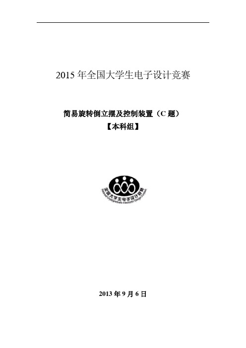
常用的电机驱动有两种方式:一、采用集成电机驱动芯片;二、采用 MOSFET 和专用栅极驱动芯片自己搭。集成主要是飞思卡尔自己生产的 33886 芯片,还有就是 L298 芯片,其中 298 是个很好的芯片,其内部可以 看成两个 H 桥,可以同时驱动两路电机,而且它也是我们驱动步进电机的 一个良选!由于他们的驱动电流较小(33886 最大 5A 持续工作,298 最大 2A 持续工作),对于我们智能车来说不足以满足,但是电子设计大赛的时 候可能会用到!所以想要详细了解他们的同学可以去查找他们的数据手册! 在此只是提供他们的电路图,不作详细介绍!
Agilent N9330B手持线缆和天线测试仪 25MHz - 4.0GHz 技术概述说明书

Agilent N9330BHandheld Cable and Antenna Tester25 MHz - 4.0 GHzTechnical OverviewYour perfect solutionfor testing cables andantennas in today’scommunication networksToday, the increasing range of wireless applications provides end users on the move with faster and more diverse services.Broadband mobile data and telephony are now becoming ubiquitous, with coverage in most urban and many rural areas.The number of base stations (BTS) needing fast, efficient installation continues to grow.Moreover, the vast numbers of existing installed base stations need periodic maintenance and, from time to time, trouble shooting and repair.Whether you do your ownmaintenance test or rely on third-party contractors, you need well-maintained antenna networks and cables to ensure:g Better voice and data quality g Fewer dropped calls g Less dropped linksAn efficient and effective cable and antenna tester is an essential basic test tool for network engineers and technicians for wireless network installation and maintenance.Key measurements Frequency domain[[[[g Return loss vs. Frequency [[[[g VSWR vs. Frequency [[[[g Cable loss test Distance to fault (DTF)[[[[g[Return loss vs. Distance [[[[g[[[[[g[VSWR vs. Fault locationDistance Easy to use and convenient to carry to any site.N9330B ApplicationsWireless service providers: base station cable & antenna system I&MAerospace and defense: radio and radar cable & antenna system I&MBroadcasting and radio links: cable & antenna system I&M Utilities, emergency and security servicesContractors for all the above•••••Verify performance and trouble-shoot base station cable and antenna systems: test wide band or narrow band from 25MHz to 4GHz:g New site installation and deploymentg Routine maintenance g Trouble shooting2Ensure the reliability of your cable andantenna systemEarly identification of potential problemsDeteriorating cable and antenna conditions, such as a loose or corroded connector, a pinched or restricted cable, or damaged lightning arrestors cause measurable RF impedance changes. Slight changes in VSWR, power loss and antenna bandwidth drift are early indications of system deterioration.Fast measurement speed means your technicians can evaluate one of the trouble spots in a matter of minutes.N9330B speeds up installation of cables and antennas at new site, too.Whatever your tasks, speed is important, with N9330B you can test more sites perday. And USB data storage lets you save all of the results for post-test analysis.You will find the Agilent N9330B tester useful and reliable, in rugged fieldenvironments for rapid installation of a new cellular network infrastructure, 2-way radio communication system or any type of communication system.Early identification of potential problemsDistance-To-Fault testing uses frequency domain reflectrometry (FDR) techniques that readily detects and locates theses slight changes in RF impedance. With routine DTF testing as part of apreventative maintenance plan, you can find and fix these problems before the system fails and repairs become costly. Agilent’s N9330B provides fast startupseconds.It's small size and light weight make it field use and all weather conditions.3A fast job, well doneA busy technician needs fast tester setup, quick calibration, and a straightforward, repeatable test procedure. Agilent N9330B gives you:Easier operationThe Agilent N9330B is easy to use, so itminimizes the need for training.Technicianswill get up to speed fast - and get theirwork done quickly.Smart, fast calibrationAt the start of any new test setup, a three-step calibration is necessary, using an open,a short, and a calibrated test load.The most accurate calibration method isto use mechanical calibration standards, anoptional special 'T-combo' open/shot/load,makes it easy for use in the field.For fast and automatic calibration, youcan choose the N9330B-203electroniccalibrator. Simply connect the electroniccalibrator and press a key to run theelectronic calibration.Well organized front-panel with more hard buttonsand function keys for faster access to essential testfunctions.'T-combo'open/short/50 ohm loadElectronic calibrator4USB memory stick supportUSB connectivity for PC softwareFast startup timeAuto calibrationTest set-up recallMore direct-access hard keysRapid cursor control and markermovement using scroll knobEasy data storageCustomized, unmistakably nameddata files and auto-sequential filenamingComprehensive results saved in aan easy-to-use formatAuto pass/fail test comparisonsN9330B-203The optimum combination of hardkeysand softkeys provides an intuitiveinterface for all measurements.The most-used functions are convenientlyselectable, via large, front-panel keys.The front-panel knob provides a simplescroll function, allowing rapid cursormovement to access data points acrossscan displays, or data entries.N9330B optimized usability:Long battery lifeModern USB connectivitySunlight-viewable LCDMulti-language UIRugged design for field usePowerful functions:Smart and fast electroniccalibratorPowerful post analysis PCsoftwareUse sensible archive file names related to each site tested The N9330B lets you choose meaningful names for your stored data: names that you customize and relate to your site. You no longer have to tolerate anonymous file names with no linkage to your site. It is easy to recognise and recall archived data files without the need for cross-referencing.And you can use sequential file names as you store successive files. Powerful PC based post analysis softwareEffective cable and antenna testing is more than just the measurements.Agilent provides a powerful PCbased post-analysis tool. This software tool, standard with every Agilent N9330B, provides trace analysis, trace comparison,customized reports and data file management.The USB connection makes it fast and easy to transfer the measurement data to the PC for analysis.Store data and setup configuration For fast instrument set up, you can store up to 15 stored configurations in the internal memory.When you take the tester out into the field, and have a large number of sites and installations to check, you need sufficient storage capacity for previous, historic data. The internal memory stores up to 200 traces, and you can save screen images.If you need even more, simply use a USB memory stick for external storage of configurations, traces and screen images.Pressing the front panel “Save” function key displays the soft key, “Save DATA as”. This then allows you to enter an appropriate file name.Take a closer look and see where Agilent puts the emphasis on usabilitySubsequently, press the “Save DATA” soft key,each new file name automatically increments, as in example:CHICAG_SITE2, CHICAG_SITE3,...5Fast export of data via USB interface6Agilent TechnologiesN9330B Handheld Cable and Antenna TesterAgilent TechnologiesN9330B Handheld Cable and Antenna TesterModern USB connectivity for both remote controland memory stickRapid marker positioning to measurementpoints using the fast-scroll rotary controlEasy results comparison-fast recall of stored dataEasy access to most common tests andsettings using keypad7Agilent reliable field useTesting in the field means workingin remote locations and out in the open: sometimes carrying test equipment up towers, or possibly workingin small, cramped buildings with no direct access to AC power on site.You may have to test:under temperature extremes in bright sunlight or in the dark in poor weather conditions None of these is the bestoperating environment for precision electronic test equipment.Agilent designed the N9330B cable and antenna tester for all weather conditions.•••Outstanding display technology provides superior performance under the most demanding lighting conditionsCarry-case options provide safe, comfortable transportThe soft carrying case provides added protection. A convenient shoulder strap leaves hands free for carrying other tools and equipment, or for safe climbing of access towers and gangways.For further protection of the tester when storing or transporting it in more harsh environments, an optional hard transit case is available.The tester itself has a strong hand strap for a sure grip when carried without the case.See traces clearly indoors and outdoorsAs with all the newest Agilent portable field equipment, operating under challenging bright sunlight or other difficult natural lighting conditions is not a problem. The bright new 6.5’’ TFT display with resolution of 640 x 480 pixels provides a superior,bright and clear trace for indoor and outdoor use.8N e wBack-lit keys for night useThe new back-lit keys in the N9330B make it easy to see the keys clearly, even in the dark.The user can adjust the brightness of the keys and the duration of the key light, making it easy to use in light or dark, day or night.N ewLow-cost, with Agilent worldwide supportSuperior battery performance Earlier battery technology used in some There is often no convenient conventional AC power line connection available at remote BTS or antenna sites. portable testers allowed only limited tester operating time before needing recharging.Worldwide service support Of course, when you buy an Agilent tester,you are confident that should you need it you have the best worldwide support.Based on customer inputs, Agilent understands that good battery life is essential for remote, on-site testing.Agilent N9330B incorporates advanced battery pack technology with intelligent charging technology, to provide you with up to four hours of continuous use. When extended operation is necessary, you simply switch batteries which only takes seconds.The long-life lithium-ion batteries in the N9330B have no 'memory', which is an important improvement over earlier battery types.To maximise useful instrument test time when on site, each tester incorporatessmart power management to help conserve battery power.The Agilent N9330B Cable and Antenna Tester - The newest in Agilent’s lineup of low cost handheld instruments.9N9330B Handheld Cable and Antenna Tester SpecificationsT est functionsFrequency Range Frequency Resolution:Output Power:Measurement Speed:Number of Data Points:Return Loss :SWR:Cable Loss:Measurement Accuracy:Distance-to-Fault:Range:Resolution:Markers:User storage:GeneralDisplay:6.5" 640x480 transflective color LCD with adjustable backlightInstrument setup storage:Trace data storage:Screen images storage:up to 15up to 200 traces 10 screensSupport USB memory stick for instrument setup, trace data and screen image storage Resolution (meter)=(1.5 x 10 )x (Vp)/(f2-f1)HzWhere Vp is the cable's relative propagation velocity.where f2 is the stop frequency and f1 is start frequency.(Number of data points - 1) x Resolution Number of data points=521,261, or 131Vertical Range:Return Loss: 0.00 to 60.00 dB SWR 1.00 to 65.00> 42 dB corrected directivity after mechanical calibration Range:Resolution:0.00 to 30.00 dB 0.01 dBRange:Accuracy:Resolution: 1.00 to 65.00same as RL 0.01Range:Accuracy:D:RL:Resolution:0.00 to 60.00dBA=20×log10(1.1+10 +0.016×10 +10 )directivity of calibrator return loss value of DUT 0.01 dB (maximun): 521(selectable 521,261,131)<2 second / screen (full span,521 data point ) (CW sweep mode)(3.0 ms/data point,typically)0~-20 dBm100 KHz 25 MHz to 4.0 GHz Return loss SWR Cable lossDistance-to-fault(DTF)6Internal user flash memory:10(-(D-RL)/20)(-RL/20)(-3+RL/20)8> 38 dB corrected directivity after electronic calibrationElectromagnetic Compatibility:IEC 61326-1:1997+A1:CISPR 11:1990/EN 55011:IEC 61000-4-2:1995+A1:IEC 61000-4-3:IEC 61000-4-4:IEC 61000-4-5:IEC 61000-4-6:IEC 61000-4-11:Canada:Australia/New Zealand:1998/EN 61326-1:1997+A1:19981991 Group 1 Class A1998/EN 61000-4-2:1995(ESD 4kV CD,8kV AD)1995/EN 61000-4-3:1995(3V/m,80% AM)1995/EN 61000-4-4:1995(EFT 0.5kV line-line,1kV line-earth)1995/EN 61000-4-5:1995(Surge 0.5kV line-line,1kV line-earth)1996/EN 61000-4-6:1996(3V ,0.15~80 MHz,80% AM,power line)1994/EN 61000-4-11:1994(Dips 1 cycle,100%)ICES-001:1998AS/NZS 2064.1IEC 61010-1:Safety:2001/EN61010-1:2001,CSA C22.2 No.61010-1:2004,UL61010-1:2004Operating:Non-operating:Temperature:-10C to 50C ,humidity 85% or less-40C to +70C (Recommend the battery be stord separately below 0 C and above +40C for any prolonged non-operating storage period.)Environmental:According to Agilent Environmental Test Manual class OE, except TemperaturePower Supply External DC Input:+11 to +25 volt dc, 40W min.Internal battery:Rechargeable Lithium-ion battery. 4 hours operating timeSize(w x h x d):Weight:Dimensions:317mm x 207 mm x 69 mm (12.5 in x 8.1 in x 2.7 in)Net weight: 2.6 kg (5.73 lbs)Weight with battery: 2.9 kg (6.39 lbs)Input and output ports:RF Test Port:Maximum Input without Damage:USB master:USB slave:Type N,female,50 +25 dBm, ±50 VDC 1 x A plug 1 x B plug v1.1 protocol v1.1 protocolSoft carrying caseN9330B handheld cable and antenna testerRechargeable batteryPhase-stable extension cableAutomotive 12V DC adaptorElectronic calibratorT-combo'open/short/50 ohm loadHard transit case11Agilent Email Updates/find/emailupdates Get the latest information on the products and applications you select.Remove all doubtOur repair and calibration services will get your equipment back to you, performing like new, when promised. You will get full value out of your Agilent equipment throughout its lifetime.Your equipment will be serviced by Agilent-trained technicians using the latest factory calibration procedures, automated repair diagnostics and genuine parts. You will always have the utmost confidence in your measurements.Agilent offers a wide range of additional expert test and measurement services for your equipment, including initial start-up assistance , onsite education and training, as well as design, system integration, and project management.For more information on repair and calibration services, go to www. /find/remove all doubtFor more information on Agilent Technologies’ products, applications or services, please contact your local Agilent office. The complete list is available at:/find/contactus Phone or Fax United States:(tel) 800 829 4444(fax) 800 829 4433Canada :(tel) 877 894 4414(fax) 800 746 4866China:(tel) 800 810 0189(fax) 800 820 2816Europe:(tel) 31 20 547 2111Japan:(tel) (81) 426 56 7832(fax) (81) 426 56 7840Product specifications and descriptions in this document subject to change without notice.© Agilent Technologies, Inc. 2008Printed in USA, July 1, 20085989-8567ENOrdering InformationModel DescriptionNumberConnectorsN9330B25 MHz to 4 GHz Handheld Cable and Antenna TesterAccessories supplied as standard with the tester: • Soft carrying case • Rechargeable battery• AC-DC adaptor with power cord • USB cable• Quick-start Tutorial• Documentation CD (also includes measurement analysis PC software)Options201202203301302303BAT 1DC 1TC ADP ABA AB2Precision mechanical short/open/50 ohm load, DC to 4 GHz Precision mechanical short/open/50 ohm load, DC to 4 GHz Electronic calibratorPhase-stable extension cable 1.5 m Phase-stable extension cable 1.5 m Connector adaptor Spare battery pack BCG External battery charger Automotive 12V DC adaptor Hard transit case Spare AC-DC adaptorHard copy English User Guide Hard copy Chinese User GuideN-type (male)7/16 DIN (male)N-type (male)Type-N (male) to type-N (female)Type-N (male) to 7/16 DIN (female)Type-N (male) to 7/16 DIN (female)Warranty and service Standard warranty is one year.R-51B-001-3C1-year return-to-Agilent warranty extended to 3-yearsCalibrationAgilent calibration upfromt support plan, 3-year coverageR-51B-001-3Korea:(tel) (080) 769 0800(fax) (080) 769 0900Latin America:(tel) (305) 269 7500Taiwan:(tel) 0800 047 866(fax) 0800 286 331Other Asia Pacific Countries:(tel) (65) 6375 8100(fax) (65) 6755 0042Email:*****************Revised: 11/08/06。
MU70-SU0 LGA2011插座R3主板 用户手册说明书

2-3-6-1 IOAT 配置...................................................................................................84
-3-
第3章
2-3-2-3 CPU T State Control(CPU T 状态控制)............................................73
2-3-3 Common RefCode Configuration(通用 RefCode 配置)..............74
2-3-5-1 内存拓扑.....................................................................................................79
2-3-5-2 内存热效应................................................................................................80
目录
包装箱物品...........................................................................................................5 MU70-SU0 主板布局..........................................................................................6 框图.......................................................................................................................9 第 1 章 硬件安装.............................................................................................10
机电综合实践开题报告

机电综合实践开题报告图1 履带式救援探索机器人示意图履带式前进系统包含三台电机,两台控制两侧履带运动,另一台用来控制鳍状肢的运动。
云台1号摄像头观察系统包含2个自由度的控制,保证最大的视角。
该机器人上安装的5自由度机械臂末端装有2号摄像头。
机械臂由旋转台,大臂,肘部,小臂,手腕组成,是一个具有五种动作的关节型机械手。
机械手动作方式可以单独行动,也可以组合或者同时进行。
可以根据控制装置来选择控制方式。
机械手的动力采用直流电机和舵机的混合搭配方式,并选择闭环控制(除舵机外)。
机械手的夹持和手腕旋转由舵机控制,其余关节由直流电机控制,全部由PWM控制。
机械手有五个自由度。
机器人的控制系统拟采用freescale的控制芯片。
这款芯片只含有8通道的PWM,由于包括运动系统部分的电机有10台,而一台电机的正反转需要2个PWM通道控制。
由于机器人、1号摄像头及机械手不是同时运动。
且只有舵机需要保持通电才能自锁。
所以,利用多组继电器,可以选择特定的电机的驱动芯片组进行控制,节约单片机I/O口资源。
并且,直流电机选定行星齿轮的减速器,在断电状态下可以自锁。
模块介绍:【机械手系统】机械手的工作原理:机械手的运动由腰部传动,上臂传动,前臂传动,肘部传动和腕部传动五部分组成。
腰部由底座上的直流电机直接传动;上臂定在腰部底板上,安装在腰部上的直流电机通过传动带动上臂左右摇摆或运动;肘部固定在上臂末端,其直流电机固定在大臂上,通过传动带动肘部;小臂固定在肘部末端,通过肘部上的直流电机传动带动小臂运动;舵机固定在小臂末端,通过传动带动手腕的转动。
【视觉系统】该机器人使用了机体上和机械臂上两个摄像头,组成视觉系统,来完成图像采集。
摄像头通过射频发送信号,接收器接收到视频信后通过视频采集器转换后,利用USB接口与PC机连接。
并在WINDOWS XP系统。
- 1、下载文档前请自行甄别文档内容的完整性,平台不提供额外的编辑、内容补充、找答案等附加服务。
- 2、"仅部分预览"的文档,不可在线预览部分如存在完整性等问题,可反馈申请退款(可完整预览的文档不适用该条件!)。
- 3、如文档侵犯您的权益,请联系客服反馈,我们会尽快为您处理(人工客服工作时间:9:00-18:30)。
BTS7970B 产品说明书 最大单脉冲电流 此图显示了最大单脉冲电流,可用于给定的脉冲时间 tpulse 驱动。最高可达电流可 以根据小电流限制水平。因为该设备的热保护,脉冲时间可能有限。
块说明及特点
芜湖蓝宙电子科技有限公司
芜湖蓝宙电子科技有限公司
BTS7970B 产品说明书 芜湖蓝宙电子科技有限公司
4.4.5真值表
BTS7970B 产品说明书
4.4.6电气特性 - 控制和诊断 芜湖蓝宙电子科技有限公司
BTS7970B 产品说明书
芜湖蓝宙电子科技有限公司
功率级 - 动态特性
BTS7970B 产品说明书
芜湖蓝宙电子科技有限公司
BTS7970B 产品说明书
4.3保护功能
该设备提供综合的保护功能。这些都是为了防止在数据手册中描述的故障情况下IC的 破坏。故障条件被视为“外”正常工作范围。保护功能不被用于连续或重复的操作与 当前的限制(第4.3.4)除外。在故障情况下的BTS7970B将应用转换率最高的转换率 电阻可以连接独立。过压,过热和过流的指示故障电流IIS(LIM)在IS引脚在一段所 述“状态标志诊断与电流检测功能”,第18和图12。
芜湖蓝宙电子科技有限公司
BTS7970B 产品说明书 在过压条件是保护处于非活动状态。 电气特性 - 保护功能 4.3.6电气特性 - 保护功能
请注意:由于过电压保护高优先级的短路保护是在过压条件无效。 芜湖蓝宙电子科技有限公司
BTS7970B 产品说明书
在下面的保护功能列在他们的优先顺序。过压锁定覆盖所有其他的错误模式。
4.3.1过压锁定
芜湖蓝宙电子科技有限公司
BTS7970B 产品说明书
为了保证对过电压高免疫力(如负载突降情况)设备闭低边MOSFET关断和打开 highside MOSFET上,如果电源电压超过过电压保护水平VOV(OFF)。该IC工作在正 常模式与滞后VOV(HY),如果再降低电源电压低于开关式电压VOV(ON)。在H桥结 构,这种行为将导致BTS7970B在highside到随心所欲的在过电压。 4.3.2欠压关机 为了避免在低电压驱动电机设备将关闭(输出三态),失控的议案如果电源电压低于 关机电压真空紫外(OFF)。该集成电路变得活跃,滞后真空紫外(HY),如果再在 电源电压上升到高于开关上的电压真空紫外(ON)。 4.3.3过热保护 输血服务中心7970B是保护,以防止过热由集成温度传感器。过热导致了两个输出级 关闭。这种状态被锁存,直到设备是由一个有TRESET最小长度在INH引脚,只要其温 度有所下降,至少在此期间,热滞后Δ T低信号复位。 在过热保护重复使用可能会减少寿命。 4.3.4电流限制 在桥的电流测量两个开关。当在一个开关(高侧或低侧)为正向电流达到极限ICLx, 此开关被关闭,另一个开关是tCLS激活。在此期间,在所有的变化
块说明及特点 中针会被忽略。然而,INH 引脚还可以用来切换两个 MOSFET 关闭。经过 tCLS 交换机 返回其初始设定。而在错误的信号引脚复位后 2 * tCLS。意外的电流限制触发短 (如由电动机来电磁干扰造成)的电流尖峰是抑制内部滤波器电路。由于阈值和过滤 器的电路反应延迟时间,有效电流限制水平 ICLx 对负载转换率取决于当前的 dI / dt,如图 10
芜湖蓝宙电子科技有限公司
•优化EMI可调摆率
BTS7970B 产品说明书
1概述
7970B 是部分 NovalithIC包含在一个芯片封装三个独立的家庭:一个 P 沟道 MOSFET 和一个 n highside 通道低边 MOSFET 驱动器 IC 一起,形成一个完全集成的高 电流半桥。所有这三个芯片安装在一个共同的引线框架,采用芯片和芯片技术芯片的 芯片。电源开关采用垂直 MOS 技术,以确保最佳状态抗性。由于 P 沟道 highside 开 关的电荷泵需要被淘汰从而减少 EMI。接口与微控制器是轻松的集成驱动 IC 功能的 逻辑电平输入,用电流检测,转换率的调整,死区时间生成和防止过热,过压,欠 压,过流和短路保护的诊断。输血服务中心 7970B 7970B 可以结合形成 H 桥和三相驱 动器配置其他基站。
7970B提供了一个受保护的高电流PWM马达具有非常低的电路板空间的消费驱动器 的成本优化的解决方案。
基本特点 •电阻的典型路径。 16毫欧@ 25°C •低静态电流的典型值。 7μ A@ 25° C •PWM能力可达25千赫的积极随心所欲组合 •开关模式电流限制在过电流降低功耗 •68一个典型电流限制水平。 / 50一分钟。 •电流检测能力现状与标志诊断 •过热关机与锁的行为了 •过压,欠压锁定 •关闭•与逻辑电平输入驱动电路
芜湖蓝宙电子科技有限公司
BTS7970B 产品说明书 芜湖蓝宙电子科技有限公司
BTS7970B 产品说明书 产品概述
7970B是一个完全集成的大电流电机驱动应用半桥。它是 NovalithIC含有一个集 成的驱动IC封装在一个一个P沟道MOSFET和一个n highside通道低边MOSFET系列的一 部分。由于P沟道highside开关的电荷泵需要被淘汰从而减少EMI。接口与微控制器是 轻松的集成驱动IC功能的逻辑电平输入,用电流检测,转换率的调整,死区时间生成 和防止过热,过压,欠压,过流和短路保护的诊断。
芜湖蓝宙电子科技有限公司
BTS7970B 产品说明书 图 9 时序图电流限制(感性负载)
芜湖蓝宙电子科技有限公司
BTS7970B 产品说明书
在一个典型的感性负载,如电机,组合,在交换模式下的电流限制这个结果。这限制 了电流的方法的优点是在 BTS7970B 功耗比驾驶线性模式 MOSFET 的小。因此,可以使 用很短的时间不超过(限制在电机启动时的浪涌电流 EG)的最大允许结温的电流限 制。然而,目前经常使用的限制只允许只要在指定的最大结温度不超标。超过这个温 度可以降低设备的使用寿命。 输出短路到接地输出短路到电源电压的负载短路 短路保护是实现了前面描述的结合电流限制与关闭的设备下过温。 4.3.5短路保护 该设备短路保护,以防止 •输出短路到地 •输出短路电源电压 •负载短路 短路保护是实现了前面描述的电流限制在 与过温关闭相结合的设备。 请注意:由于过电压保护,短路更高的优先级
芜湖蓝宙电子科技有限公司
BTS7970B 产品说明书 芜湖蓝宙电子科技有限公司
引脚配置
BTS7970B 产品说明书
引脚定义和功能 芜湖蓝宙电子科技有限公司
最大额定值
BTS7970B 产品说明书
注:最大额定值,超过其中任何一个值可能会造成不可逆转的破坏设备。接触的时间 延长在最大值条件下可能影响器件的可靠性
芜湖蓝宙电子科技有限公司
功率级 - 静态特性
BTS7970B 产品说明书
由于积极的续流,二极管导通仅几微秒,这取决于 RSR 开关时间
芜湖蓝宙电子科技有限公司
BTS7970B 产品说明书
由于为上升的时间差异和下降沿会有之间的输入脉冲长度和输出脉冲的长度略有差 异。它可以使用下列公式计算: • tHS = (tdr(HS) + 0.5 tr(HS)) - (tdf(HS) + 0.5 tf(HS)) • tLS = (tdf(LS) + 0.5 tf(LS)) - (tdr(LS) + 0.5 tr(LS)).
BTS7970B 产品说明书
4.2功率级 在BTS7970B的功率级由一个P -通道的垂直DMOS为高侧开关和低侧开关的N沟道晶 体管的垂直DMOS晶体管。所有的保护和诊断功能都位于一个单独的顶级芯片。这两
芜湖蓝宙电子科技有限公司
BTS7970B 产品说明书 个开关可以操作高达25千赫,使随心所欲的和积极的综合二极管正向操作从而最大 限度地降低功耗。 关于态电阻 RON 的是在电源电压 VS 以及对结温 Tj 依赖。对国家电阻特性典型的是 如图 6 所示。
5.热特性 芜湖蓝宙电子科技有限公司
BTS7970B 产品说明书
6. 应用
6.2由于高电流快速开关时间,要特别注意采取的PCB布局。杂散电感都必须在桥梁设 芜湖蓝宙电子科技有限公司
BTS7970B 产品说明书 计中的权力最小化,因为它是在所有的高功率开关必要桥梁。输血服务中心7970B并 没有为电源地和逻辑地单独引脚。因此,建议以确保之间的压摆率接地电阻,电流检 测电阻器和地面设备的引脚偏移(GND/引脚1)最小化。如果BTS7970B是在H -桥或B6 桥设计中,不同的设备之间的GND引脚的偏移电压要小也是如此。 一个陶瓷电容从VS到地接近每个设备,建议,为通过一个低阻抗通路开关三相电流, 从而减少噪音和地面反弹。针对此电容的合理价值大约是470 nF的。 数字输入需要从多余的电流通过串联电阻(例如,通过感应电压尖峰引起的)在 10kΩ 的范围的保护。 7.封装外形P - TO - 263 - 7
4.4控制和诊断4.4.1输入电路 IN和INH控制输入包括TTL/ CMOS兼容的控制滞后的施密特为MOSFET的栅极驱动器集成 触发器。设置INH引脚为高使能设备。在这种情况下两个电源开关一个是打开对IN引 脚的状态而定。要关闭两个开关,INH引脚被设置为低。无需外部驱动是必要的。输 血服务中心7970B接口,可直接与微控制器。 4.4.2死区时间生成 在桥的应用已经得到保证,和低边MOSFET的highside不是在同一时间进行,电池电压 直接连接到GND。这是保证,在驱动IC电路,产生了所谓的关掉一个MOSFET之间和对 其他开关的死区时间。死时间在驱动IC产生的自动调节到选定的转换率。4.4.3可调 摆率 为了优化电磁辐射,对MOSFET的开关速度是由一个外部电阻调节。压摆率SR引脚允许 用户在自己的应用程序优化通过连接一个外部电阻到GND之间RSR排放和功耗的平衡。 4.4.4电流检测能力现状与诊断标志 状态引脚用作电流检测和综合错误标志输出。在正常操作(电流检测模式),一个电 流源连接到引脚的状态,可提供的电流成比例的正向负载电流通过积极的高边开关电 流。如果高侧开关处于非活动状态或当前是在没有相反的方向流动的电流驱动,除了 轻微的泄漏电流IIS(LK)。外部电阻RIS确定每个输出电流电压。例如随着19500的 电流检测比率基利斯面值= IL/ IIS,一个RIS=1kΩ 的电阻值导致VIS=(IL /19.5 A)五 由于良好的长期稳定性和低温度系数就可以提高校准的绝对应用程序中的电流检测精 度。为达到最佳效果,建议做两点校准。 在故障状态情况下,状态输出连接到电流源是独立的负载电流,并提供 IIS (LIM)。而在 IS 引脚的最大电压是由外部电阻和电源电压的选择。在当前情况下, IIS 限制(LIM)被激活为 2 * tCLS。