89C51英文说明
文献翻译-AT89C51的介绍及运用概述

英文翻译系别专业班级学生姓名学号指导教师Introduction and application of AT89C51 Microcontrollers are used in a multitude of commercial applications such as modems, motor-control systems, air conditioner control systems, automotive engine and among others. The high processing speed and enhanced peripheral set of these microcontrollers make them suitable for such high-speed event-based applications. However, these critical application domains also require that these microcontrollers are highly reliable. The high reliability and low market risks can be ensured by a robust testing process and a proper tools environment for the validation of these microcontrollers both at the component and at the system level. Intel Plaform Engineering department developed an object-oriented multi-threaded test environment for the validation of its AT89C51 automotive microcontrollers. The goals of this environment was not only to provide a robust testing environment for the AT89C51 automotive microcontrollers, but to develop an environment which can be easily extended and reused for the validation of several other future microcontrollers. The environment was developed in conjunction with Microsoft Foundation Classes (AT89C51).The paper describes the design and mechanism of this test environment, its interactions with various hardware/software environmental components, and how to use AT89C51.1. IntroductionThe 8-bit AT89C51 CHMOS microcontrollers are designed to handle high-speed calculations and fast input/output operations. MCS 51 microcontrollers are typically used for high-speed event control systems. Commercial applications include modems, motor-control systems, printers, photocopiers, air conditioner control systems, disk drives, and medical instruments. The automotive industry use MCS 51 microcontrollers in engine-control systems, airbags, suspension systems, and antilock braking systems (ABS).The AT89C51 is especially well suited to applications that benefit from its processing speed and enhanced on-chip peripheral functions set, such as automotive power-train control, vehicle dynamic suspension, antilock braking, and stability control applications. Because of these critical applications, the market requires a reliable cost-effective controller with a low interrupt latency response, ability to service the high number of time and event driven integrated peripherals needed in real time applications, and a CPU with above average processing power in a single package. The financial and legal risk of having devices that operate unpredictably is very high. Once in the market, particularly in mission critical applications such as anautopilot or anti-lock braking system, mistakes are financially prohibitive. Redesign costs can run as high as a $500K, much more if the fix means back annotating it across a product family that share the same core and/or peripheral design flaw. In addition, field replacements of components is extremely expensive, as the devices are typically sealed in modules with a total value several times that of the component. To mitigate these problems, it is essential that comprehensive testing of the controllers be carried out at both the component level and system level under worst case environmental and voltage conditions.This complete and thorough validation necessitatesnot only a well-defined process but also a proper environment and tools to facilitate and execute the mission successfully.Intel Chandler Platform Engineering group provides postsilicon system validation (SV) of various micro-controllers and processors. The system validation process can be broken into three major parts.The type of the device and its application requirements determine which types of testing are performed on the device.The AT89C51 provides the following standard features: 4Kbytes of Flash, 128 bytes of RAM, 32 I/O lines, two 16-bittimer/counters, a five vector two-level interrupt architecture,a full duple ser -ial port, on-chip oscillator and clock circuitry.In addition, the AT89C51 is designed with static logic for operation down to zero frequency and supports two software selectable power saving modes. The Idle Mode stops the CPU while allowing the RAM, timer/counters,serial port and interrupt sys -tem to continue functioning. The Power-down Mode saves the RAM contents but freezes the oscil -lator disabling all other chip functions until the next hardware reset.Pin Configurations Block Diagram2 Pin DescriptionVCC Supply voltage.GND Ground.Port 0Port 0 is an 8-bit open-drain bi-directional I/O port. As an output port, each pin can sink eight TTL inputs. When 1s are written to port 0 pins, the pins can be used as high impedance inputs.Port 0 may also be configured to be the multiplexed low order address/data bus during accesses to external program and data memory. In this mode P0 has internal pullups.Port 0 also receives the code bytes during Flash programming, and outputs the code bytes during program verification. External pullups are required during program verification.Port 1Port 1 is an 8-bit bi-directional I/O port with internal pullups.The Port 1 output buffers can sink/so -urce four TTL inputs.When 1s are written to Port 1 pins they are pulled high by the internal pullups and can be used as inputs. As inputs, Port1 pins that are externally being pulled low will source current (IIL) because ofthe internal pullups.Port 1 also receives the low-order address bytes during Flash programming and verification.Port 2Port 2 is an 8-bit bi-directional I/O port with internal pullups.The Port 2 output buffers can sink/source four TTL inputs.When 1s are written to Port 2 pins they are pulled high by the internal pullups and can be used as inputs. As inputs, Port 2 pins that are externally being pulled low will source current (IIL) because of the internal pullups.Port 2 emits the high-order address byte during fetches from external program memory and during accesses to Port 2 pins that are externally being pulled low will source current (IIL) because of the internal pullups.Port 2 emits the high-order address byte during fetches from external program memory and during accesses to external data memory that use 16-bit addresses (MOVX @DPTR). In this application, it uses strong internal pull-ups when emitting 1s.During accesses to external data memory that use 8-bit addresses (MOVX @ RI), Port 2 emitsthe contents of the P2 Special Function Register.Port 2 also receives the high-order address bits and some control signals durin Flash programming and verification.Port 3Port 3 is an 8-bit bi-directional I/O port with internal pullups.The Port 3 output buffers can sink/sou -rce four TTL inputs.When 1s are written to Port 3 pins they are pulled high by the internal pullups and can be used as inputs. As inputs,Port 3 pins that are externally being pulled low will source current (IIL) because of the pullups. Port 3 also serves the functions of various special featuresof the AT89C51 as listed below:3 Port Pin Alternate FunctionsP3.0 RXD(serial input port)P3.1 TXD (serial output port)P3.2 INT0 (external interrupt 0)P3.3 INT1 (external interrupt 1)P3.4 T0 (timer 0 external input)P3.5 T1 (timer 1 external input)P3.6 WR (external data memory write strobe)P3.7 RD (external data memory read strobe)Port 3 also receives some control signals for Flash programming and verification. RSTReset input. A high on this pin for two machine cycles while the oscillator is running resets the device.ALE/PROGAddress Latch Enable output pulse for latching the low byte of the address during accesses to external memory. This pin is also the program pulse input (PROG)during Flash programming.In normal operation ALE is emitted at a constant rate of 1/6 the oscillator frequency, and may be used for external timing or clocking purposes. Note, however, that one ALE pulse is skipped duri -ng each access to external DataMemory.If desired, ALE operation can be disabled by setting bit 0 of SFR location 8EH. With the bit set, ALE is active only during a MOVX or MOVC instruction. Otherwise, the pin is weakly pulled high. Setting the ALE-disable bit has no effect if the microcontroller is in external execution mode.PSENProgram Store Enable is the read strobe to external program memory. When the AT89C51 is executing code from external program memory, PSEN is activated twice each machine cycle, except that two PSEN activations are skipped during each access to external data memory.EA/VPPExternal Access Enable. EA must be strapped to GND in order to enable the device to fetch code from external program memory locations starting at 0000H up to FFFFH. Note, however, that if lock bit 1 is programmed, EA will be internally latched on reset.EA should be strapped to VCC for internal program executions. This pin also receives the 12-volt programming enable voltage (VPP) during Flash programming, for parts that require 12-volt VPP.XTAL1Input to the inverting oscillator amplifier and input to the internal clock operating circuit.XTAL2Output from the inverting oscillator amplifier.4 Oscillator CharacteristicsXTAL1 and XTAL2 are the input and output, respectively, of an inverting amplifier which can be configured for use as an on-chip oscillator, as shown in Figure 1. Either a quartz crystal or ceramic resonator may be used. To drive the device from an external clock source, XTAL2 should be left unconnected while XTAL1 is driven as shown in Figure 2.There are no requirements on the duty cycle of the external clock signal, since the input to the internal clocking circuitry is through a divide-by-two flip-flop, but minimum and maximum voltage high and low time specifications must be observed.Idle ModeIn idle mode, the CPU puts itself to sleep while all the onchip peripherals remain active. The mode is invoked by software. The content of the on-chip RAM and all the special functions registers remain unchanged during this mode. The idle mode can be terminated by any enabled interrupt or by a hardware reset. It should be noted that when idle is terminated by a hard ware reset, the device normally resumes program execution, from where it left off, up to two machine cycles before the internal reset algorithm takes control. On-chip hardware inhibits access to internal RAM in this event, but access to the port pins is not inhibited. To eliminate the possibility of an unexpected write to a port pin when Idle is terminated by reset, theinstruction following the one that invokes Idle should not be one that writes to a port pin or to external memory.Figure 1. Oscillator Connections Figure 2. External Clock Drive Configuration Note: C1, C2 = 30 pF . .10 pF for Crystals = 40 pF . .10 pF for Ceramic Resonators In the power-down mode, the oscillator is stopped, and the instruction that invokes.5 Power-down Modepower-down is the last instruction executed. The on-chip RAM and Special Function Registers retain their values until the power-down mode is terminated. The only exit from power-down is a hardware reset. Reset redefines the SFRs but does not change the on-chip RAM. The reset should not be activated before VCC is restored to its normal operating level and must be held active long enough to allow the oscillator to restart and stabilize.Status of External Pins During Idle and Power-down Modes Mode Program Memory ALE PSEN PORT0 PORT1 PORT2 PORT3Idle Internal 1 1 Data Data Data DataIdle External 1 1 Float Data Address DataPower-down Internal 0 0 Data Data Data DataPower-down External 0 0 Float Data Data DataProgram Memory Lock BitsOn the chip are three lock bits which can be left unprogrammed (U) or can be programmed (P) to obtain the additional features listed in the table below.Lock Bit Protection Modes Program Lock Bits Protection Type LB1 LB2 LB31 U U U No program lock features2 P U U MOVC instructions executed from external program memory are disabled from etching code bytes from internal memory.3 P P U Same as mode 2, also verify is disabled4 P P P Same as mode 3, also external execution is disabledWhen lock bit 1 is programmed, the logic level at the EA pin is sampled and latched during reset. If the device is powered up without a reset, the latch initializes to a random value, and holds that value until reset is activated. It is necessary that the latched value of EA be in agreement with the current logic level at that pin in order for the device to function properly.6 Programming the FlashThe AT89C51 is normally shipped with the on-chip Flash memory array in the erased state (that is, contents = FFH) and ready to be programmed. The programming interface accepts either a high-voltage (12-volt) or a low-voltage (VCC) program enable signal. The low-voltage programming mode provides a convenient way to program the AT89C51 inside the user’s system, while the high-voltage programming mode is compatible with conventional thirdparty Flash or EPROM programmers. The AT89C51 is shipped with either the high-voltage or low-voltage programming mode enabled. The respective top-side marking and device signature codes are listed in the following table.VPP = 12V VPP = 5VTop-Side Mark AT89C51 AT89C51xxxx xxxx-5yyww yywwSignature (030H) = 1EH (030H) = 1EH(031H) = 51H (031H) = 51H(032H) =F FH (032H) = 05HThe AT89C51 code memory array is programmed byte-bybyte in either programming mode. To program any nonblank byte in the on-chip Flash Memory, the entire memory must be erased using the Chip Erase Mode.7 Programming AlgorithmBefore programming the AT89C51, the address, data and control signals should be set up according to the Flash programming mode table and Figure 3 and Figure 4. To program the AT89C51, take the following steps.1. Input the desired memory location on the address lines.2. Input the appropriate data byte on the data lines.3. Activate the correct combination of control signals.4. Raise EA/VPP to 12V for the high-voltage programming mode.5. Pulse ALE/PROG once to program a byte in the Flash array or the lock bits. The byte-write cycle is self-timed and typically takes no more than 1.5 ms. Repeat steps 1 through 5, changing the address and data for the entire array or until the end of the object file is reached.Data Polling:The AT89C51 features Data Polling to indicate the end of a write cycle. During a write cycle, an attempted read of the last byte written will result in the complement of the written datum on PO.7. Once the write cycle has been completed, true data are valid on all outputs, and the next cycle may begin. Data Polling may begin any time after a write cycle has been initiated.Ready/Busy:The progress of byte programming can also be monitored by the RDY/BSY output signal. P3.4 is pulled low after ALE goes high during programming to indicate BUSY. P3.4 is pulled high again when programming is done to indicateREADY.Program Verify: If lock bits LB1 and LB2 have not been programmed, the programmed code data can be read back via the address and data lines for verification.The lock bits cannot be verified directly. Verification of the lock bits is achieved by observing that their features are enabled.8 Flash Programming ModesMode RST PSEN ALE/PROG EA/VPP P2.6 P2.7 P3.6 P3.7Write Code Data H L H/12V L H H HRead Code Data H L H H L L H HWriteLockBit -1 H L H/12V H H H HBit -2 H L H/12V H H L LBit -3 H L H/12V H L L LChip Erase H LH/12V H L L LRead Signature Byte H L H H L L L LNote: 1. Chip Erase requires a 10 ms PROG pulse.Figure 3. Programming the Flash Figure 4. Verifying the FlashFlash Programming and Verification Waveforms -High-voltage Mode (VPP = 12V) Flash Programming and Verification Waveforms -Low-voltage Mode (VPP = 5V)9 Chip EraseThe entire Flash array is erased electrically by using the proper combination of control signals and by holding ALE/PROG low for 10 ms. The code array is written with all “1”s. The chip erase operation must be executed befor e the code memory can be re-programmed.Reading the Signature Bytes:The signature bytes are read by the same procedure as a normal verification of locations 030H, 031H, and 032H, except that P3.6 and P3.7 must be pulled to a logic low. The values returned areas follows.(030H) = 1EH indicates manufactured by Atmel(031H) = 51H indicates 89C51(032H) = FFH indicates 12V programming(032H) = 05H indicates 5V programmingProgramming InterfaceEvery code byte in the Flash array can be written and the entire array can be erased by using the appropriate combination of control signals. The write operation cycle is selftimed and once initiated, will automatically time itself to completion. Flash Programming and Verification Characteristics TA = 0°C to 70°C, VCC = 5.0 . .10%10 Symbol Parameter Min Max UnitsVPP(1) Programming EnableV oltage11.5 12.5 VIPP(1) Programming Enable Current 1.0 mA1/tCLCL Oscillator Frequency 3 24 MHztA VGL Address Setup to PROGLow48tCLCLtGHAX Address Hold After PROG 48tCLCLtDVGL Data Setup to PROG Low 48tCLCLtGHDX Data Hold After PROG 48tCLCLtEHSH P2.7(ENABLE) High to VPP 48tCLCLtSHGL VPP Setup to PROG Low 10 μstGHSL(1) VPP Hold After PROG 10 μstGLGH PROG Width 1 110 μstA VQV Address to Data Valid 48tCLCLtELQV ENABLE Low to Data Valid 48tCLCLtEHQZ Data Float After ENABLE 0 48tCLCLtGHBL PROG High to BUSY Low 1.0 μstWC Byte Write Cycle Time 2.0 msNote: 1. Only used in 12-volt programming mode.Absolute Maximum Ratings*Operating Temperature......................... -55°C to +125°CStorage Temperature ............................. -65°C to +150°CV oltage on Any Pin with Respect to Ground ............-1.0V to +7.0VMaximum Operating V oltage .................................. 6.6VDC Output Current....................................... 15.0 mA11 DC CharacteristicsTA = -40°C to 85°C, VCC = 5.0V . .20% (unless otherwise noted)Symbol Parameter Condition Min Max Units VIL Input Low-voltage (Except EA) -0.5 0.2 VCC 0.1 -VVIL1 nput Low-voltage (EA) -0.5 0.2 VCC 0.3 -VVIH iput High-voltage (Except XTAL1, RST) 0.2 VCC +0.9 VCC + 0.5 VVIH1 Input High-voltage (XTAL1, RST) 0.7 VCC VCC + 0.5 VVOL Output Low-voltage(1) (Ports 1,2,3) IOL = 1.6 mA 0.45 VVOL1 Output Low-voltage(1) (Port 0, ALE, PSEN) IOL = 3.2 mA 0.45 VVOH Output High-voltage (Ports 1,2,3, ALE, PSEN) IOH = -60 μA, VCC = 5V . .10% 2.4 VIOH = -25 μA 0.75 VCC VIOH = -10 μA 0.9 VCC VVOH1 Output High-voltage (Port 0 in External Bus Mode) IOH = -800 μA, VCC = 5V . .10% 2.4 VIOH = -300μA, 0.75 VCC VIOH = -80μA, 0.9 VCC VIIL Logical 0 Input Current (Ports 1,2,3)VIN = 0.45V -50 μ AITL Logical 1 to 0 Transition Current (Ports 1,2,3) VIN = 2V, VCC = 5V . .10% -650 μ AILI Input Leakage Current (Port 0, EA) 0.45 < VIN < VCC . 10 μ A RRST Reset Pull-down Resistor 50 300 K.CIO Pin Capacitance Test Freq. = 1 MHz, TA = 25°C 10 pFICC Power Supply Current Active Mode, 12 MHz 20 mA Idle Mode, 12 MHz 5 mA Power-down Mode(2) VCC = 6V 100 μ A VCC = 3V 40 μ A12 AC CharacteristicsUnder operating conditions, load capacitance for Port 0, ALE/PROG, and PSEN = 100 pF; load capacitance for all other outputs = 80 pF.External Program and Data Memory Characteristics Symbol ParameterFrequency 12 MHz Oscillator 16 to 24 MHz Oscillator Units Min Max Min Max 1/tCLCL Oscillator 0 24 MHztLHLL ALE Pulse Width 127 2tCLCL-40 40 ns nstA VLL Address Valid to ALE Low 43 tCLCL-13 nstLLAX Address Hold After ALE Low 48 tCLCL-20 nstLLIV ALE Low to Valid Instruction In 233 4tCLCL-65 nstLLPL ALE Low to PSEN Low 43 tCLCL-13 nstPLPH PSEN Pulse Width 205 3tCLCL-20 nstPLIV PSEN Low to Valid Instruction In 145 3tCLCL-45 nstPXIX Input Instruction Hold After PSEN 0 0 nstPXIZ Input Instruction Float After PSEN 59 tCLCL-10 nstPXA V PSEN to Address Valid 75 tCLCL-8 nstA VIV Address to Valid Instruction In 312 5tCLCL-55 nstPLAZ PSEN Low to Address Float 10 10 nstRLRH RD Pulse Width 400 6tCLCL-100 nstWLWH WR Pulse Width 400 6tCLCL-100 nstRLDV RD Low to Valid Data In 252 5tCLCL-90 nstRHDX Data Hold After RD 0 0 ns 13tRHDZ Data Float After RD 97 2tCLCL-28 nstLLDV ALE Low to Valid Data In 517 8tCLCL-150 nstA VDV Address to Valid Data In 585 9tCLCL-165 nstLLWL ALE Low to RD or WR Low 200 300 3tCLCL-50 3tCLCL+50 nstA VWL Address to RD or WR Low 203 4tCLCL-75 nstQVWX Data Valid to WR Transition 23 tCLCL-20 nstQVWH Data Valid to WR High 433 7tCLCL-120 nstWHQX Data Hold After WR 33 tCLCL-20 nstRLAZ RD Low to Address Float 0 0 nstWHLH RD or WR High to ALE High 43 123 tCLCL-20 nsExternal Program Memory Read CycleExternal Data Memory Read CycleExternal Data Memory Write Cycle External Data Memory Write CycleExternal Clock Drive WaveformsExternal Clock DriveSymbol Parameter Min Max Units1/tCLCL Oscillator Frequency 0 24 MHztCLCL Clock Period 41.6 nstCHCX High Time 15 nstCLCX Low Time 15 nstCLCH Rise Time 20 nstCHCL Fall Time ns 20 nsSerial Port Timing:Shift Register Mode Test Conditions(VCC = 5.0 V . .20%; Load Capacitance = 80 pF)Symbol Parameter 12 MHz Osc Variable Oscillator Units UnitsMin Max Min MaxtXLXL Serial Port Clock Cycle Time 1.0 12tCLCL μstQVXH Output Data Setup to Clock Rising Edge 700 10tCLCL-133 nstXHQX Output Data Hold After Clock Rising Edge 50 2tCLCL-117 nstXHDX Input Data Hold After Clock Rising Edge 0 0 nstXHDV Clock Rising Edge to Input Data Valid 700 10tCLCL-133 ns 13 ShiftRegister Mode Timing Waveforms AC Testing Input/Output Waveforms Float WaveformsA microcomputer interface converts information between two forms. Outside the microcomputer the information handled by an electronic system exists as a physical signal, but within the program, it is represented numerically. The function of any interface can be broken down into a number of operations which modify the data in some way, so that the process of conversion between the external and internal forms is carried out in a number of steps.An analog-to-digital converter(ADC) is used to convert a continuously variable signal to a corresponding digital form which can take any one of a fixed number of possible binary values. If the output of the transducer does not vary continuously, no ADC is necessary. In this case the signal conditioning section must convert the incoming signal to a form which can be connected directly to the next part of the interface, the input/output section of the microcomputer itself.Output interfaces take a similar form, the obvious difference being that here the flow of information is in the opposite direction; it is passed from the program to the outside world. In this case the program may call an output subroutine which supervises the operation of the interface and performs the scaling numbers which may be needed for a digital-to-analog converter(DAC). This subroutine passes information in turn to an output device which produces a corresponding electrical signal, which could be converted into analog form using a DAC. Finally the signal is conditioned(usually amplified) to a form suitable for operating an actuator.The signals used within microcomputer circuits are almost always too small to be connected directly to the “outside world” and some kind of interface must be used to translate them to a more appropriate form. The design of section of interface circuits is one of the most important tasks facing the engineer wishing to apply microcomputers. We have seen that in microcomputers information is represented as discrete patterns of bits; this digital form is most useful when the microcomputer is to be connected to equipment which can only be switched on or off, where each bit might represent the state of a switch or actuator.To solve real-world problems, a microcontroller must have more than just a CPU, a program, and a data memory. In addition, it must contain hardware allowing the CPU to access information from the outside world. Once the CPU gathers information and processes the data, it must also be able to effect change on some portion of the outside world.These hardware devices, called peripherals, are the CPU’s window to theoutside. The most basic form of peripheral available on microcontrollers is the general purpose I70 port. Each of the I/O pins can be used as either an input or an output. The function of each pin is determined by setting or clearing corresponding bits in a corresponding data direction register during the initialization stage of a program. Each output pin may be driven to either a logic one or a logic zero by using CPU instructions to pin may be viewed (or read.) by the CPU using program instructions.Some type of serial unit is included on microcontrollers to allow the CPU to communicate bit-serially with external devices. Using a bit serial format instead of bit-parallel format requires fewer I/O pins to perform the communication function, which makes it less expensive, but slower. Serial transmissions are performed either synchronously or asynchronously.AT89C51的介绍及运用单片机广泛应用于商业:诸如调制解调器,电动机控制系统,空调控制系统,汽车发动机和其他一些领域。
关于单片机at89c51的外文翻译5000字英文

关于单片机at89c51的外文翻译5000字英文篇一:毕业设计外文翻译单片机AT89C51附件1:外文资料翻译译文AT89C51主要性能参数:与MCS-51产品如前所述完全兼容4K字节可重檫写Flash闪速存储器1000次檫写周期全静态操作:0HZ-24MHZ三级加密程序存储器128*8字节内部RAM32个可编程I/O口线2个16位定时/记数器6个中断源可编程串行UART通道低功耗空闲和掉电操作方式功能特性概述:AT89C51提供更多以下标准功能:4K字节Flash闪速存储器,128字节内部RAM,32个I/O口线,两个16位定时/记数器,一个5向量两级中断结构,一个全双工串行通信口,片内振荡器妥善钟电路。
同时,AT89C51可降至0HZ的静态逻辑操作,并支持两种软件可选的节电工作模式。
空闲方式停止CPU的工作,但允许RAM,定时/记数器,串行通信口及中断系统继续工作。
掉电方式保存RAM中的内容,但振荡器停止工作直到下一个硬件逊位。
AT89C51是美国ATMEL公司生产的低电压,高性能CMOS8位单片机,片内含4k bytes的可反复擦写的只读程序存储器(PEROM)和128 bytes的随机存取数据存储器(RAM),器件采用ATMEL公司的高密度、非易失性存储技术生产,兼容标准MCS-51指令系统,片内置通用8位中央处理器(CPU)和Flash存储单元,功能强大AT89C51单片机用法可为您提供许多高性价比的应用场合,可灵活科技领域应用于各种支配领域。
AT89C51方框图引脚功能说明·Vcc:电源电压·GND:地·P0 口:P0 口是一组8 位漏极开路型双向I/O 口,也即地址/数据总线复用口。
作为输出口用时,每位能吸收电流的方式驱动8个TTL逻辑门电路,对端口写“1”可作为差阻抗输入端用。
在访问外部数据存储器或程序存储器时,这组口线分时转换地址(低8位)和数据总线复用,在访问期间激活内部上拉电阻。
89C51单晶片接脚简介

89C51單晶片接腳簡介The 89C51 is a CMOS 8-bit microcomputer with 4K bytes of Flash programmable and erasable read only memory (PEROM). We want to develop embedded control applications for the robot system of the telepresence agent project. For example, 89C51 can control motors with wireless devices. A PC can transmit data to 89C51 via RS232 serial port for controlling, communicating or receiving. This document is a basic introduction to 89C51.1. 89C51單晶片簡介圖1所示為89C51單晶片接腳圖,此單晶片由ATMEL公司所製造,可重複燒錄1000次以上。
89C51單晶片必須供應電壓,電源接腳為VCC(pin40)、GND(pin20),工作電壓在4V~6.6V之間,建議使用+5V電源供應器,可保持單晶片工作壽命。
圖1. 89C51單晶片接腳圖【1】89C51單晶片接腳簡介如下:PORT0PORT0包括P0.0~P0.7(pin39~pin32),主要有記憶體擴充位址∕資料匯流排、燒錄時的資料碼輸入與輸出、以及一般I/O等三個功能。
PORT1PORT1包括P1.0~P1.7(pin1~pin8),有燒錄時的低位元組位址與一般I/O 兩個功能。
PORT2PORT2包括P2.0~P2.7(pin21~pin28),有記憶體擴充時的高位元組位址匯流排、燒錄時的控制功能、以及一般I/O等三個功能。
89c51datasheet

SCON Address = 98H Reset Value = 0000 0000B Bit AddressableSM0/FE SM1SM2REN TB8RB8Tl RlBit:76543210(SMOD0 = 0/1)*Symbol FunctionFE Framing Error bit. This bit is set by the receiver when an invalid stop bit is detected. The FE bit is not cleared by valid frames but should be cleared by software. The SMOD0 bit must be set to enable access to the FE bit.SM0Serial Port Mode Bit 0, (SMOD0 must = 0 to access bit SM0)SM1Serial Port Mode Bit 1SM0SM1Mode Description Baud Rate**000shift register f OSC/120118-bit UART variable1029-bit UART f OSC/64 or f OSC/321139-bit UART variableSM2Enables the Automatic Address Recognition feature in Modes 2 or 3. If SM2 = 1 then Rl will not be set unless the received 9th data bit (RB8) is 1, indicating an address, and the received byte is a Given or Broadcast Address.In Mode 1, if SM2 = 1 then Rl will not be activated unless a valid stop bit was received, and the received byte is aGiven or Broadcast Address. In Mode 0, SM2 should be 0.REN Enables serial reception. Set by software to enable reception. Clear by software to disable reception.TB8The 9th data bit that will be transmitted in Modes 2 and 3. Set or clear by software as desired.RB8In modes 2 and 3, the 9th data bit that was received. In Mode 1, if SM2 = 0, RB8 is the stop bit that was received.In Mode 0, RB8 is not used.Tl Transmit interrupt flag. Set by hardware at the end of the 8th bit time in Mode 0, or at the beginning of the stop bit in the other modes, in any serial transmission. Must be cleared by software.Rl Receive interrupt flag. Set by hardware at the end of the 8th bit time in Mode 0, or halfway through the stop bit time in the other modes, in any serial reception (except see SM2). Must be cleared by software.NOTE:*SMOD0 is located at PCON6.**f OSC = oscillator frequency SU00043Figure 7. SCON: Serial Port Control RegisterPX0IP (0B8H)Priority Bit = 1 assigns higher priorityPriority Bit = 0 assigns lower priorityBIT SYMBOL FUNCTIONIP .7—Not implemented, reserved for future use.IP .6—Not implemented, reserved for future use.IP .5PT2Timer 2 interrupt priority bit.IP .4PS Serial Port interrupt priority bit.IP .3PT1Timer 1 interrupt priority bit.IP .2PX1External interrupt 1 priority bit.IP .1PT0Timer 0 interrupt priority bit.IP .0PX0External interrupt 0 priority bit.SU00572PT0PX1PT1PS PT2——01234567Figure 11. IP RegistersPX0HIPH (B7H)Priority Bit = 1 assigns higher priorityPriority Bit = 0 assigns lower priorityBIT SYMBOL FUNCTIONIPH.7—Not implemented, reserved for future use.IPH.6—Not implemented, reserved for future use.IPH.5PT2H Timer 2 interrupt priority bit high.IPH.4PSH Serial Port interrupt priority bit high.IPH.3PT1H Timer 1 interrupt priority bit high.IPH.2PX1H External interrupt 1 priority bit high.IPH.1PT0H Timer 0 interrupt priority bit high.IPH.0PX0H External interrupt 0 priority bit high.SU01058PT0H PX1H PT1H PSH PT2H ——01234567Figure 12. IPH RegistersPLCC44:plastic leaded chip carrier; 44 leads SOT187-2DIP40:plastic dual in-line package; 40 leads (600 mil)SOT129-1QFP44:plastic quad flat package; 44 leadsNOTESDefinitionsShort-form specification — The data in a short-form specification is extracted from a full data sheet with the same type number and title. For detailed information see the relevant data sheet or data handbook.Limiting values definition — Limiting values given are in accordance with the Absolute Maximum Rating System (IEC 134). Stress above one or more of the limiting values may cause permanent damage to the device. These are stress ratings only and operation of the device at these or at any other conditions above those given in the Characteristics sections of the specification is not implied. Exposure to limiting values for extended periods may affect device reliability.Application information — Applications that are described herein for any of these products are for illustrative purposes only. Philips Semiconductors make no representation or warranty that such applications will be suitable for the specified use without further testing or modification.DisclaimersLife support — These products are not designed for use in life support appliances, devices or systems where malfunction of these products can reasonably be expected to result in personal injury. Philips Semiconductors customers using or selling these products for use in such applications do so at their own risk and agree to fully indemnify Philips Semiconductors for any damages resulting from such application.Right to make changes — Philips Semiconductors reserves the right to make changes, without notice, in the products, including circuits, standard cells, and/or software, described or contained herein in order to improve design and/or performance. Philips Semiconductors assumes no responsibility or liability for the use of any of these products, conveys no license or title under any patent, copyright, or mask work right to these products, and makes no representations or warranties that these products are free from patent, copyright, or mask work right infringement, unless otherwise specified.Philips Semiconductors811 East Arques AvenueP.O. Box 3409Sunnyvale, California 94088–3409Telephone 800-234-7381© Copyright Philips Electronics North America Corporation 1999All rights reserved. Printed in U.S.A.Date of release: 10-99。
PHILIPS 89C51RB2 89C51RC2 89C51RD2 说明书

Philips Semiconductors Preliminary specification 89C51RB2/89C51RC2/89C51RD280C51 8-bit Flash microcontroller family 16KB/32KB/64KB ISP/IAP Flash with 512B/512B/1KB RAM DESCRIPTION The 89C51RB2/RC2/RD2 device contains a non-volatile16kB/32kB/64kB Flash program memory that is both parallel programmable and serial In-System and In-Application Programmable. In-System Programming (ISP) allows the user to download new code while the microcontroller sits in the application.In-Application Programming (IAP) means that the microcontroller fetches new program code and reprograms itself while in the system. This allows for remote programming over a modem link.A default serial loader (boot loader) program in ROM allows serialIn-System programming of the Flash memory via the UART without the need for a loader in the Flash code. For In-Application Programming, the user program erases and reprograms the Flashmemory by use of standard routines contained in ROM.This device executes one machine cycle in 6 clock cycles, hence providing twice the speed of a conventional 80C51. An OTPconfiguration bit lets the user select conventional 12 clock timing if desired.This device is a Single-Chip 8-Bit Microcontroller manufactured in advanced CMOS process and is a derivative of the 80C51microcontroller family. The instruction set is 100% compatible with the 80C51 instruction set.The device also has four 8-bit I/O ports, three 16-bit timer/eventcounters, a multi-source, four-priority-level, nested interrupt structure,an enhanced UART and on-chip oscillator and timing circuits.The added features of the P89C51RB2/RC2/RD2 makes it apowerful microcontroller for applications that require pulse width modulation, high-speed I/O and up/down counting capabilities such as motor control.FEATURES•80C51 Central Processing Unit•On-chip Flash Program Memory with In-System Programming (ISP) and In-Application Programming (IAP) capability•Boot ROM contains low level Flash programming routines for downloading via the UART•Can be programmed by the end-user application (IAP)•6 clocks per machine cycle operation (standard)•12 clocks per machine cycle operation (optional)•Speed up to 20 MHz with 6 clock cycles per machine cycle(40 MHz equivalent performance); up to 33 MHz with 12 clocksper machine cycle•Fully static operation•RAM expandable externally to 64 kB•4 level priority interrupt•8 interrupt sources•Four 8-bit I/O ports•Full-duplex enhanced UART–Framing error detection–Automatic address recognition•Power control modes–Clock can be stopped and resumed–Idle mode–Power down mode•Programmable clock out•Second DPTR register•Asynchronous port reset•Low EMI (inhibit ALE)•Programmable Counter Array (PCA)–PWM–Capture/compareORDERING INFORMATIONPHILIPS(EXCEPT NORTH PHILIPSNORTH MEMORYTEMPERATUREVOLTAGEFREQUENCY (MHz)AMERICA) PART ORDERNUMBER PART MARKINGAMERICAPART ORDERNUMBERFLASH RAM RANGE (°C)AND PACKAGE RANGE6 CLOCKMODE12 CLOCKMODEDWG #1P89C51RB2HBP P89C51RB2BP16 kB512 B0 to +70, PDIP 4.5–5.5 V0 to 20 MHz0 to 33 MHz SOT129-1 2P89C51RB2HFP P89C51RB2FP16 kB512 B–40 to +85, PDIP 4.5–5.5 V0 to 20 MHz0 to 33 MHz SOT129-1 3P89C51RB2HBA P89C51RB2BA16 kB512 B0 to +70, PLCC 4.5–5.5 V0 to 20 MHz0 to 33 MHz SOT187-2 4P89C51RB2HFA P89C51RB2FA16 kB512 B–40 to +85, PLCC 4.5–5.5 V0 to 20 MHz0 to 33 MHz SOT187-2 5P89C51RB2HBB P89C51RB2BB16 kB512 B0 to +70, PQFP 4.5–5.5 V0 to 20 MHz0 to 33 MHz SOT307-2 6P89C51RB2HFB P89C51RB2FB16 kB512 B–40 to +85, PQFP 4.5–5.5 V0 to 20 MHz0 to 33 MHz SOT307-2 7P89C51RC2HBP P89C51RC2BP32 kB512 B0 to +70, PDIP 4.5–5.5 V0 to 20 MHz0 to 33 MHz SOT129-1 8P89C51RC2HFP P89C51RC2FP32 kB512 B–40 to +85, PDIP 4.5–5.5 V0 to 20 MHz0 to 33 MHz SOT129-1 9P89C51RC2HBA P89C51RC2BA32 kB512 B0 to +70, PLCC 4.5–5.5 V0 to 20 MHz0 to 33 MHz SOT187-2 10P89C51RC2HFA P89C51RC2FA32 kB512 B–40 to +85, PLCC 4.5–5.5 V0 to 20 MHz0 to 33 MHz SOT187-2 11P89C51RC2HBB P89C51RC2BB32 kB512 B0 to +70, PQFP 4.5–5.5 V0 to 20 MHz0 to 33 MHz SOT307-2 12P89C51RC2HFB P89C51RC2FB32 kB512 B–40 to +85, PQFP 4.5–5.5 V0 to 20 MHz0 to 33 MHz SOT307-2 13P89C51RD2HBP P89C51RD2BP64 kB 1 kB0 to +70, PDIP 4.5–5.5 V0 to 20 MHz0 to 33 MHz SOT129-1 14P89C51RD2HFP P89C51RD2FP64 kB 1 kB–40 to +85, PDIP 4.5–5.5 V0 to 20 MHz0 to 33 MHz SOT129-1 15P89C51RD2HBA P89C51RD2BA64 kB 1 kB0 to +70, PLCC 4.5–5.5 V0 to 20 MHz0 to 33 MHz SOT187-2 16P89C51RD2HFA P89C51RD2FA64 kB 1 kB–40 to +85, PLCC 4.5–5.5 V0 to 20 MHz0 to 33 MHz SOT187-2 17P89C51RD2HBB P89C51RD2BB64 kB 1 kB0 to +70, PQFP 4.5–5.5 V0 to 20 MHz0 to 33 MHz SOT307-2 18P89C51RD2HFB P89C51RD2FB64 kB 1 kB–40 to +85, PQFP 4.5–5.5 V0 to 20 MHz0 to 33 MHz SOT307-2BLOCK DIAGRAMSU01065PSEN EAV PP ALE RST XTAL1XTAL2V CCV SSPORT 0DRIVERS PORT 2DRIVERS RAM ADDR REGISTER RAM PORT 0LATCH PORT 2LATCH FLASHREGISTER BACC STACKPOINTER TMP2TMP1ALU TIMING AND CONTROL IN S T R U C TI ONREGIS TERPD OSCILLATORPSW PORT 1LATCH PORT 3LATCHPORT 1 DRIVERS PORT 3DRIVERS PROGRAMADDRESSREGISTER BUFFERPCINCRE-MENTER PROGRAM COUNTERDPTR’SMULTIPLEP1.0–P1.7P3.0–P3.7P0.0–P0.7P2.0–P2.7SFRsTIMERSP .C.A.8816LOGIC SYMBOL PO RT 0P ORT 1P O R T 2P O R T3ADDRESS AND DATA BUS ADDRESS BUST2T2EXRxDTxDINT0INT1T0T1WR RD S E C O N D A R Y F U N C T I O N S RST EA/V PP PSEN ALE/PROG V SSV CC XTAL1XTAL2SU01302PINNING Plastic Dual In-Line Package12345678910111213141516171819202122232425262728293031323334353637383940T2/P1.0T2EX/P1.1ECI/P1.2CEX0/P1.3CEX1/P1.4CEX2/P1.5CEX3/P1.6RST RxD/P3.0TxD/P3.1INT0/P3.2INT1/P3.3T0/P3.4T1/P3.5CEX4/P1.7WR/P3.6RD/P3.7XTAL2XTAL1V SS P2.0/A8P2.1/A9P2.2/A10P2.3/A11P2.4/A12P2.5/A13P2.6/A14P2.7/A15PSEN ALE/PROG EA/V PP P0.7/AD7P0.6/AD6P0.5/AD5P0.4/AD4P0.3/AD3P0.2/AD2P0.1/AD1P0.0/AD0V CCDUAL IN-LINE PACKAGE SU00021Plastic Leaded Chip CarrierLCC614071739291828Pin Function 1NIC*2P1.0/T23P1.1/T2EX 4P1.2/ECI 5P1.3/CEX06P1.4/CEX17P1.5/CEX28P1.6/CEX39P1.7/CEX410RST 11P3.0/RxD 12NIC*13P3.1/TxD 14P3.2/INT015P3.3/INT1Pin Function 16P3.4/T017P3.5/T118P3.6/WR 19P3.7/RD 20XTAL221XTAL122V SS 23NIC*24P2.0/A825P2.1/A926P2.2/A1027P2.3/A1128P2.4/A1229P2.5/A1330P2.6/A14Pin Function31P2.7/A1532PSEN33ALE/PROG34NIC*35EA/VPP36P0.7/AD737P0.6/AD638P0.5/AD539P0.4/AD440P0.3/AD341P0.2/AD242P0.1/AD143P0.0/AD044V CCSU00023* NO INTERNAL CONNECTION Plastic Quad Flat PackPQFP443411133231222Pin Function1P1.5/CEX22P1.6/CEX33P1.7/CEX44RST 5P3.0/RxD 6NIC*7P3.1/TxD 8P3.2/INT09P3.3/INT110P3.4/T011P3.5/T112P3.6/WR 13P3.7/RD 14XTAL215XTAL1Pin Function 16V SS 17NIC*18P2.0/A819P2.1/A920P2.2/A1021P2.3/A1122P2.4/A1223P2.5/A1324P2.6/A1425P2.7/A1526PSEN 27ALE/PROG 28NIC*29EA/V PP 30P0.7/AD7Pin Function31P0.6/AD632P0.5/AD533P0.4/AD434P0.3/AD335P0.2/AD236P0.1/AD137P0.0/AD038V CC39NIC*40P1.0/T241P1.1/T2EX42P1.2/ECI43P1.3/CEX044P1.4/CEX1SU00024* NO INTERNAL CONNECTIONPIN DESCRIPTIONSPIN NUMBERNAME AND FUNCTIONMNEMONICPDIP PLCC PQFPTYPE NAME AND FUNCTIONV SS202216I Ground: 0 V reference.V CC404438I Power Supply: This is the power supply voltage for normal, idle, and power-downoperation.P0.0–0.739–3243–3637–30I/O Port 0: Port 0 is an open-drain, bidirectional I/O port. Port 0 pins that have 1swritten to them float and can be used as high-impedance inputs. Port 0 is also themultiplexed low-order address and data bus during accesses to external programand data memory. In this application, it uses strong internal pull-ups when emitting 1s.P1.0–P1.71–82–940–44,1–3I/O Port 1: Port 1 is an 8-bit bidirectional I/O port with internal pull-ups on all pins except P1.6 and P1.7 which are open drain. Port 1 pins that have 1s written to them are pulled high by the internal pull-ups and can be used as inputs. As inputs, port 1 pins that are externally pulled low will source current because of the internalpull-ups. (See DC Electrical Characteristics: I IL).Alternate functions for 89C51RB2/RC2/RD2 Port 1 include:1240I/O T2 (P1.0): Timer/Counter 2 external count input/Clockout (see ProgrammableClock-Out)2341I T2EX (P1.1): Timer/Counter 2 Reload/Capture/Direction Control3442I ECI (P1.2): External Clock Input to the PCA4543I/O CEX0 (P1.3): Capture/Compare External I/O for PCA module 05644I/O CEX1 (P1.4): Capture/Compare External I/O for PCA module 1671I/O CEX2 (P1.5): Capture/Compare External I/O for PCA module 2782I/O CEX3 (P1.6): Capture/Compare External I/O for PCA module 3893I/O CEX4 (P1.7): Capture/Compare External I/O for PCA module 4P2.0–P2.721–2824–3118–25I/O Port 2: Port 2 is an 8-bit bidirectional I/O port with internal pull-ups. Port 2 pins thathave 1s written to them are pulled high by the internal pull-ups and can be used asinputs. As inputs, port 2 pins that are externally being pulled low will source currentbecause of the internal pull-ups. (See DC Electrical Characteristics: I IL). Port 2emits the high-order address byte during fetches from external program memoryand during accesses to external data memory that use 16-bit addresses (MOVX@DPTR). In this application, it uses strong internal pull-ups when emitting 1s.During accesses to external data memory that use 8-bit addresses (MOV @Ri),port 2 emits the contents of the P2 special function register.P3.0–P3.710–1711,13–195, 7–13I/O Port 3: Port 3 is an 8-bit bidirectional I/O port with internal pull-ups. Port 3 pins that have 1s written to them are pulled high by the internal pull-ups and can be used asinputs. As inputs, port 3 pins that are externally being pulled low will source currentbecause of the pull-ups. (See DC Electrical Characteristics: I IL). Port 3 also servesthe special features of the 89C51RB2/RC2/RD2, as listed below:10115I RxD (P3.0): Serial input port11137O TxD (P3.1): Serial output port12148I INT0 (P3.2): External interrupt13159I INT1 (P3.3): External interrupt141610I T0 (P3.4): Timer 0 external input151711I T1 (P3.5): Timer 1 external input161812O WR (P3.6): External data memory write strobe171913O RD (P3.7): External data memory read strobeRST9104I Reset: A high on this pin for two machine cycles while the oscillator is running,resets the device. An internal diffused resistor to V SS permits a power-on resetusing only an external capacitor to V CC.ALE303327O Address Latch Enable: Output pulse for latching the low byte of the addressduring an access to external memory. In normal operation, ALE is emitted twiceevery machine cycle, and can be used for external timing or clocking. Note that oneALE pulse is skipped during each access to external data memory. ALE can bedisabled by setting SFR auxiliary.0. With this bit set, ALE will be active only during aMOVX instruction.MNEMONIC NAME AND FUNCTIONTYPE PIN NUMBERPQFP PLCC PDIP PSEN 293226O Program Store Enable: The read strobe to external program memory. Whenexecuting code from the external program memory, PSEN is activated twice eachmachine cycle, except that two PSEN activations are skipped during each accessto external data memory. PSEN is not activated during fetches from internalprogram memory.EA/V PP 313529I External Access Enable/Programming Supply Voltage: EA must be externallyheld low to enable the device to fetch code from external program memorylocations. If EA is held high, the device executes from internal program memory.The value on the EA pin is latched when RST is released and any subsequentchanges have no effect. This pin also receives the programming supply voltage(V PP ) during Flash programming.XTAL1192115I Crystal 1: Input to the inverting oscillator amplifier and input to the internal clockgenerator circuits.XTAL2182014O Crystal 2: Output from the inverting oscillator amplifier.NOTE:To avoid “latch-up” effect at power-on, the voltage on any pin (other than V PP ) must not be higher than V CC + 0.5 V or less than V SS – 0.5 V.Table 1.Special Function RegistersSYMBOL DESCRIPTIONDIRECTADDRESSBIT ADDRESS, SYMBOL, OR ALTERNATIVE PORT FUNCTIONMSB LSBRESETVALUEACC*Accumulator E0H E7E6E5E4E3E2E1E000H AUXR#Auxiliary8EH––––––EXTRAM AO xxxxxx10B AUXR1#Auxiliary 1A2H––ENBOOT–GF20–DPS xxxxxxx0B B* B register F0H F7F6F5F4F3F2F1F000H CCAP0H#Module 0 Capture High FAH xxxxxxxxB CCAP1H#Module 1 Capture High FBH xxxxxxxxB CCAP2H#Module 2 Capture High FCH xxxxxxxxB CCAP3H#Module 3 Capture High FDH xxxxxxxxB CCAP4H#Module 4 Capture High FEH xxxxxxxxB CCAP0L#Module 0 Capture Low EAH xxxxxxxxB CCAP1L#Module 1 Capture Low EBH xxxxxxxxB CCAP2L#Module 2 Capture Low ECH xxxxxxxxB CCAP3L#Module 3 Capture Low EDH xxxxxxxxB CCAP4L#Module 4 Capture Low EEH xxxxxxxxBCCAPM0#Module 0 Mode DAH–ECOM CAPP CAPN MAT TOG PWM ECCF x0000000B CCAPM1#Module 1 Mode DBH–ECOM CAPP CAPN MAT TOG PWM ECCF x0000000B CCAPM2#Module 2 Mode DCH–ECOM CAPP CAPN MAT TOG PWM ECCF x0000000B CCAPM3#Module 3 Mode DDH–ECOM CAPP CAPN MAT TOG PWM ECCF x0000000B CCAPM4#Module 4 Mode DEH–ECOM CAPP CAPN MAT TOG PWM ECCF x0000000BDF DE DD DC DB DA D9D8CCON*#PCA Counter Control D8H CF CR–CCF4CCF3CCF2CCF1CCF000x00000B CH#PCA Counter High F9H00HCL#PCA Counter Low E9H00H CMOD#PCA Counter Mode D9H CIDL WDTE–––CPS1CPS0ECF00xxx000B DPTR:Data Pointer (2 bytes)DPH Data Pointer High83H00H DPL Data Pointer Low82H00HAF AE AD AC AB AA A9A8IE*Interrupt Enable 0A8H EA EC ET2ES ET1EX1ET0EX000HBF BE BD BC BB BA B9B8IP*Interrupt Priority B8H–PPC PT2PS PT1PX1PT0PX0x0000000BB7B6B5B4B3B2B1B0IPH#Interrupt Priority High B7H–PPCH PT2H PSH PT1H PX1H PT0H PX0H x0000000B8786858483828180P0*Port 080H AD7AD6AD5AD4AD3AD2AD1AD0FFH9796959493929190P1*Port 190H CEX4CEX3CEX2CEX1CEX0ECI T2EX T2FFHA7A6A5A4A3A2A1A0P2*Port 2A0H AD15AD14AD13AD12AD11AD10AD9AD8FFHB7B6B5B4B3B2B1B0P3*Port 3B0H RD WR T1T0INT1INT0TxD RxD FFHPCON#1Power Control87H SMOD1SMOD0––GF1GF0PD IDL00xxx000B *SFRs are bit addressable.#SFRs are modified from or added to the 80C51 SFRs.–Reserved bits.1.Reset value depends on reset source.Table 1.Special Function Registers (Continued)SYMBOL DESCRIPTIONDIRECTADDRESSBIT ADDRESS, SYMBOL, OR ALTERNATIVE PORT FUNCTIONMSB LSBRESETVALUE D7D6D5D4D3D2D1D0PSW*Program Status Word D0H CY AC F0RS1RS0OV F1P00000000B RCAP2H#Timer 2 Capture High CBH00H RCAP2L#Timer 2 Capture Low CAH00HSADDR#Slave Address A9H00H SADEN#Slave Address Mask B9H00HSBUF Serial Data Buffer99H xxxxxxxxB9F9E9D9C9B9A9998SCON*Serial Control98H SM0/FE SM1SM2REN TB8RB8TI RI00HSP Stack Pointer81H07H8F8E8D8C8B8A8988TCON*Timer Control88H TF1TR1TF0TR0IE1IT1IE0IT000HCF CE CD CC CB CA C9C8T2CON*Timer 2 Control C8H TF2EXF2RCLK TCLK EXEN2TR2C/T2CP/RL200HT2MOD#Timer 2 Mode Control C9H––––––T2OE DCEN xxxxxx00B TH0Timer High 08CH00HTH1Timer High 18DH00HTH2#Timer High 2CDH00HTL0Timer Low 08AH00HTL1Timer Low 18BH00HTL2#Timer Low 2CCH00H TMOD Timer Mode89H GATE C/T M1M0GATE C/T M1M000H WDTRST Watchdog Timer Reset A6H*SFRs are bit addressable.#SFRs are modified from or added to the 80C51 SFRs.–Reserved bits.OSCILLATOR CHARACTERISTICSXTAL1 and XTAL2 are the input and output, respectively, of an inverting amplifier. The pins can be configured for use as anon-chip oscillator.To drive the device from an external clock source, XTAL1 should be driven while XTAL2 is left unconnected. Minimum and maximum high and low times specified in the data sheet must be observed. This device is configured at the factory to operate using 6 clock periods per machine cycle, referred to in this datasheet as “6 clock mode”. (This yields performance equivalent to twice that of standard 80C51 family devices). It may be optionally configured on commercially-available EPROM programming equipment to operate at 12 clocks per machine cycle, referred to in this datasheet as “12 clock mode”. Once 12 clock mode has been configured, it cannot be changed back to 6 clock mode.RESETA reset is accomplished by holding the RST pin high for at least two machine cycles (12 oscillator periods in 6 clock mode, or 24 oscillator periods in 12 clock mode), while the oscillator is running. To ensure a good power-on reset, the RST pin must be high long enough to allow the oscillator time to start up (normally a few milliseconds) plus two machine cycles. At power-on, the voltage on V CC and RST must come up at the same time for a proper start-up. Ports 1, 2, and 3 will asynchronously be driven to their reset condition when a voltage above V IH1 (min.) is applied to RESET.The value on the EA pin is latched when RST is deasserted and has no further effect.LOW POWER MODESStop Clock ModeThe static design enables the clock speed to be reduced down to0 MHz (stopped). When the oscillator is stopped, the RAM and Special Function Registers retain their values. This mode allows step-by-step utilization and permits reduced system power consumption by lowering the clock frequency down to any value. For lowest power consumption the Power Down mode is suggested. Idle ModeIn the idle mode (see Table 2), the CPU puts itself to sleep while all of the on-chip peripherals stay active. The instruction to invoke the idle mode is the last instruction executed in the normal operating mode before the idle mode is activated. The CPU contents, theon-chip RAM, and all of the special function registers remain intact during this mode. The idle mode can be terminated either by any enabled interrupt (at which time the process is picked up at the interrupt service routine and continued), or by a hardware reset which starts the processor in the same manner as a power-on reset. Power-Down ModeTo save even more power, a Power Down mode (see Table 2) can be invoked by software. In this mode, the oscillator is stopped and the instruction that invoked Power Down is the last instruction executed. The on-chip RAM and Special Function Registers retain their values down to 2.0 V and care must be taken to return V CC to the minimum specified operating voltages before the Power Down Mode is terminated.Either a hardware reset or external interrupt can be used to exit from Power Down. Reset redefines all the SFRs but does not change the on-chip RAM. An external interrupt allows both the SFRs and theon-chip RAM to retain their values.To properly terminate Power Down, the reset or external interrupt should not be executed before V CC is restored to its normal operating level and must be held active long enough for the oscillator to restart and stabilize (normally less than 10 ms).With an external interrupt, INT0 and INT1 must be enabled and configured as level-sensitive. Holding the pin low restarts the oscillator but bringing the pin back high completes the exit. Once the interrupt is serviced, the next instruction to be executed after RETI will be the one following the instruction that put the device into Power Down. POWER OFF FLAGThe Power Off Flag (POF) is set by on-chip circuitry when the V CC level on the 89C51RB2/RC2/RD2 rises from 0 to 5 V. The POF bit can be set or cleared by software allowing a user to determine if the reset is the result of a power-on or a warm start after powerdown. The V CC level must remain above 3 V for the POF to remain unaffected by the V CC level.Design Consideration•When the idle mode is terminated by a hardware reset, the device normally resumes program execution, from where it left off, up to two machine cycles before the internal reset algorithm takes control. On-chip hardware inhibits access to internal RAM in this event, but access to the port pins is not inhibited. To eliminate the possibility of an unexpected write when Idle is terminated by reset, the instruction following the one that invokes Idle should not be one that writes to a port pin or to external memory.ONCE™ ModeThe ONCE (“On-Circuit Emulation”) Mode facilitates testing and debugging of systems without the device having to be removed from the circuit. The ONCE Mode is invoked by:1.Pull ALE low while the device is in reset and PSEN is high;2.Hold ALE low as RST is deactivated.While the device is in ONCE Mode, the Port 0 pins go into a float state, and the other port pins and ALE and PSEN are weakly pulled high. The oscillator circuit remains active. While the device is in this mode, an emulator or test CPU can be used to drive the circuit. Normal operation is restored when a normal reset is applied. Programmable Clock-OutA 50% duty cycle clock can be programmed to come out on P1.0. This pin, besides being a regular I/O pin, has two alternate functions. It can be programmed:1.to input the external clock for Timer/Counter 2, or2.to output a 50% duty cycle clock ranging from 122 Hz to 8 MHz ata 16 MHz operating frequency (61 Hz to 4 MHz in 12 clock mode). To configure the Timer/Counter 2 as a clock generator, bit C/T2 (inT2CON) must be cleared and bit T20E in T2MOD must be set. Bit TR2 (T2CON.2) also must be set to start the timer.The Clock-Out frequency depends on the oscillator frequency and the reload value of Timer 2 capture registers (RCAP2H, RCAP2L) as shown in this equation:Oscillator Frequencyn(65536*RCAP2H,RCAP2L)n = 2 in 6 clock mode4 in 12 clock modeWhere (RCAP2H,RCAP2L) = the content of RCAP2H and RCAP2L taken as a 16-bit unsigned integer.In the Clock-Out mode Timer 2 roll-overs will not generate an interrupt. This is similar to when it is used as a baud-rate generator. It is possible to use Timer 2 as a baud-rate generator and a clock generator simultaneously. Note, however, that the baud-rate and the Clock-Out frequency will be the same.Table 2.External Pin Status During Idle and Power-Down ModeMODE PROGRAM MEMORY ALE PSEN PORT 0PORT 1PORT 2PORT 3 Idle Internal11Data Data Data Data Idle External11Float Data Address Data Power-down Internal00Data Data Data Data Power-down External00Float Data Data DataTIMER 2 OPERATIONTimer 2Timer 2 is a 16-bit Timer/Counter which can operate as either an event timer or an event counter, as selected by C/T2* in the special function register T2CON (see Figure 1). Timer 2 has three operating modes: Capture, Auto-reload (up or down counting), and Baud Rate Generator, which are selected by bits in the T2CON as shown inT able 3.Capture ModeIn the capture mode there are two options which are selected by bit EXEN2 in T2CON. If EXEN2=0, then timer 2 is a 16-bit timer or counter (as selected by C/T2* in T2CON) which, upon overflowing sets bit TF2, the timer 2 overflow bit. This bit can be used to generate an interrupt (by enabling the Timer 2 interrupt bit in theIE register). If EXEN2= 1, Timer 2 operates as described above, but with the added feature that a 1- to -0 transition at external inputT2EX causes the current value in the Timer 2 registers, TL2 andTH2, to be captured into registers RCAP2L and RCAP2H, respectively. In addition, the transition at T2EX causes bit EXF2 in T2CON to be set, and EXF2 like TF2 can generate an interrupt (which vectors to the same location as Timer 2 overflow interrupt. The Timer 2 interrupt service routine can interrogate TF2 and EXF2 to determine which event caused the interrupt). The capture mode is illustrated in Figure 2 (There is no reload value for TL2 and TH2 in this mode. Even when a capture event occurs from T2EX, the counter keeps on counting T2EX pin transitions or osc/6 pulses (osc/12 in 12 clock mode).).Auto-Reload Mode (Up or Down Counter)In the 16-bit auto-reload mode, Timer 2 can be configured (as either a timer or counter [C/T2* in T2CON]) then programmed to count up or down. The counting direction is determined by bit DCEN (Down Counter Enable) which is located in the T2MOD register (see Figure 3). When reset is applied the DCEN=0 which means Timer 2 will default to counting up. If DCEN bit is set, Timer 2 can count up or down depending on the value of the T2EX pin.Figure 4 shows Timer 2 which will count up automatically since DCEN=0. In this mode there are two options selected by bit EXEN2 in T2CON register. If EXEN2=0, then Timer 2 counts up to 0FFFFH and sets the TF2 (Overflow Flag) bit upon overflow. This causes the Timer 2 registers to be reloaded with the 16-bit value in RCAP2L and RCAP2H. The values in RCAP2L and RCAP2H are preset by software means.If EXEN2=1, then a 16-bit reload can be triggered either by an overflow or by a 1-to-0 transition at input T2EX. This transition also sets the EXF2 bit. The Timer 2 interrupt, if enabled, can be generated when either TF2 or EXF2 are 1.In Figure 5 DCEN=1 which enables Timer 2 to count up or down. This mode allows pin T2EX to control the direction of count. When a logic 1 is applied at pin T2EX Timer 2 will count up. Timer 2 will overflow at 0FFFFH and set the TF2 flag, which can then generate an interrupt, if the interrupt is enabled. This timer overflow also causes the 16-bit value in RCAP2L and RCAP2H to be reloaded into the timer registers TL2 and TH2.When a logic 0 is applied at pin T2EX this causes Timer 2 to count down. The timer will underflow when TL2 and TH2 become equal to the value stored in RCAP2L and RCAP2H. Timer 2 underflow sets the TF2 flag and causes 0FFFFH to be reloaded into the timer registers TL2 and TH2.The external flag EXF2 toggles when Timer 2 underflows or overflows. This EXF2 bit can be used as a 17th bit of resolution if needed. The EXF2 flag does not generate an interrupt in this mode of operation.(MSB)(LSB)Symbol Position Name and SignificanceTF2T2CON.7Timer 2 overflow flag set by a Timer 2 overflow and must be cleared by software. TF2 will not be set when either RCLK or TCLK = 1.EXF2T2CON.6Timer 2 external flag set when either a capture or reload is caused by a negative transition on T2EX and EXEN2 = 1. When Timer 2 interrupt is enabled, EXF2 = 1 will cause the CPU to vector to the Timer 2interrupt routine. EXF2 must be cleared by software. EXF2 does not cause an interrupt in up/downcounter mode (DCEN = 1).RCLK T2CON.5Receive clock flag. When set, causes the serial port to use Timer 2 overflow pulses for its receive clock in modes 1 and 3. RCLK = 0 causes Timer 1 overflow to be used for the receive clock.TCLK T2CON.4Transmit clock flag. When set, causes the serial port to use Timer 2 overflow pulses for its transmit clock in modes 1 and 3. TCLK = 0 causes Timer 1 overflows to be used for the transmit clock.EXEN2T2CON.3Timer 2 external enable flag. When set, allows a capture or reload to occur as a result of a negative transition on T2EX if Timer 2 is not being used to clock the serial port. EXEN2 = 0 causes Timer 2 toignore events at T2EX.TR2T2CON.2Start/stop control for Timer 2. A logic 1 starts the timer.C/T2T2CON.1Timer or counter select. (Timer 2)0 = Internal timer (OSC/6 in 6 clock mode or OSC/12 in 12 clock mode)1 = External event counter (falling edge triggered).CP/RL2T2CON.0Capture/Reload flag. When set, captures will occur on negative transitions at T2EX if EXEN2 = 1. When cleared, auto-reloads will occur either with Timer 2 overflows or negative transitions at T2EX whenEXEN2 = 1. When either RCLK = 1 or TCLK = 1, this bit is ignored and the timer is forced to auto-reloadon Timer 2 overflow.TF2EXF2RCLK TCLK EXEN2TR2C/T2CP/RL2SU01251Figure 1. Timer/Counter 2 (T2CON) Control Register。
89C51数据手册

阅读数据手册是一个工程师的必备技能,拿到 一份数据手册,特别是英文数据手册,如何去读 ,才能更快更好的找到自己想要的东西,归纳如 下: (1)检查手册发布的日期; (2)General Description:一般性描述,但有时 也会给出一些其他资料中没有提及的特性或用 法; (3)Feature:提供常规特性信息,确认电器特 性所在的条件以及特殊情况;
4.认真研读芯片内部寄存器,对寄存器的理解 程度,直接决定了你对该芯片的掌握程度。必 须清楚它们上电后的初始值、所能实现的功能 、每个bit所代表的含义这些基本情况。 5.仔细研究手册给出的时序图,这是对芯片进 行正确操作的关键。单个信号的周期、上升时 间、下降时间、建立时间、保持时间,以及信 号之间的相位关系 6.提醒“note”,必须仔细阅读,一般这都是能 否正确使用、或能否把芯片用好的关键之所在
(8) Absolute Maxium Ratings:给出极限范围;
(9) Electrical Characteristics:给出电气规范;
(10) Typical Performance Characteristics:给 出一些特性曲线; (11)Applications Information:给出示例电路 和使用注意。
1.先看芯片的特性(Features)、应用场合 (Applications)以及内部框图。这有助于我们对 芯片有一个宏观的了解。 2.重点关注芯片的参数,同时可以参考手册给 出的一些参数图 3.选定器件后,研究芯片管脚定义、推荐的 PCB layout,这些都是在硬件设计过程中必须 掌握的。这是将来用好该芯片的前提。
1.plastic leaded chip carrier ——带引线的塑料芯片载体(PLCC),表面贴 装型封装之一 2.Plastic Dual In-Line Package(DIP)双 列直插型 3.Plastic Quat Flat Pack——塑胶四方扁 平封装 4.
AT_89C51中英文翻译资料
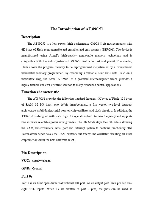
The Introduction of AT 89C51DescriptionThe AT89C51 is a low-power, high-performance CMOS 8-bit microcomputer with 4K bytes of Flash programmable and erasable read only memory (PEROM). The device is manufactured using Atmel’s high-density nonvolatile memory technology and is compatible with the industry-standard MCS-51 instruction set and pinout. The on-chip Flash allows the program memory to be reprogrammed in-system or by a conventional nonvolatile memory programmer. By combining a versatile 8-bit CPU with Flash on a monolithic chip, the Atmel AT89C51 is a powerful microcomputer which provides a highly-flexible and cost-effective solution to many embedded control applications. Function characteristicThe AT89C51 provides the following standard features: 4K bytes of Flash, 128 bytes of RAM, 32 I/O lines, two 16-bit timer/counters, a five vector two-level interrupt architecture, a full duplex serial port, on-chip oscillator and clock circuitry. In addition, the AT89C51 is designed with static logic for operation down to zero frequency and supports two software selectable power saving modes. The Idle Mode stops the CPU while allowing the RAM, timer/counters, serial port and interrupt system to continue functioning. The Power-down Mode saves the RAM contents but freezes the oscillator disabling all other chip functions until the next hardware reset.Pin DescriptionVCC:Supply voltage.GND:Ground.Port 0:Port 0 is an 8-bit open-drain bi-directional I/O port. As an output port, each pin can sink eight TTL inputs. When 1s are written to port 0 pins, the pins can be used ashighimpedance inputs. Port 0 may also be configured to be the multiplexed loworder address/data bus during accesses to external program and data memory. In this mode P0 has internal pullups. Port 0 also receives the code bytes during Flash programming, and outputs the code bytes during program verification. External pullups are required during program verification.Port 1Port 1 is an 8-bit bi-directional I/O port with internal pullups. The Port 1 output buffers can sink/source four TTL inputs. When 1s are written to Port 1 pins they are pulled high by the internal pullups and can be used as inputs. As inputs, Port 1 pins that are externally being pulled low will source current (IIL) because of the internal pullups. Port 1 also receives the low-order address bytes during Flash programming and verification.Port 2Port 2 is an 8-bit bi-directional I/O port with internal pullups. The Port 2 output buffers can sink/source four TTL inputs. When 1s are written to Port 2 pins they are pulled high by the internal pullups and can be used as inputs. As inputs, Port 2 pins that are externally being pulled low will source current, because of the internal pullups. Port 2 emits the high-order address byte during fetches from external program memory and during accesses to external data memory that use 16-bit addresses. In this application, it uses strong internal pullupswhen emitting 1s. During accesses to external data memory that use 8-bit addresses, Port 2 emits the contents of the P2 Special Function Register. Port 2 also receives the high-order address bits and some control signals during Flash programming and verification.Port 3Port 3 is an 8-bit bi-directional I/O port with internal pullups. The Port 3 output buffers can sink/source four TTL inputs. When 1s are written to Port 3 pins they are pulled high by the internal pullups and can be used as inputs. As inputs, Port 3 pins that are externally being pulled low will source current (IIL) because of the pullups. Port 3 also- 2 -serves the functions of variousspecial features of the AT89C51 as listed below:RSTReset input. A high on this pin for two machine cycles while the oscillator is running resets the device.ALE/PROGAddress Latch Enable output pulse for latching the low byte of the address during accesses to external memory. This pin is also the program pulse input (PROG) during Flash programming. In normal operation ALE is emitted at a constant rate of 1/6 the oscillator frequency, and may be used for external timing or clocking purposes. Note, however, that one ALE pulse is skipped during each access to external Data Memory.If desired, ALE operation can be disabled by setting bit 0 of SFR location 8EH. With the bit set, ALE is active only during a MOVX or MOVC instruction. Otherwise, the pin is weakly pulled high. Setting the ALE-disable bit has no effect if the microcontroller is in external execution mode.PSENProgram Store Enable is the read strobe to external program memory. When theAT89C51 is executing code from external program memory, PSEN is activated twice each- 3 -machine cycle, except that two PSEN activations are skipped during each access to external data memory.EA/VPPExternal Access Enable. EA must be strapped to GND in order to enable the device to fetch code from external program memory locations starting at 0000H up to FFFFH. Note, however, that if lock bit 1 is programmed, EA will be internally latched on reset.EA should be strapped to VCC for internal program executions. This pin also receives the 12-volt programming enable voltage(VPP) during Flash programming, for parts that require12-volt VPP.XTAL1Input to the inverting oscillator amplifier and input to the internal clock operating circuit.XTAL2Out put from the inverting oscillator amplifier.Oscillator CharacteristicsXTAL1 and XTAL2 are the input and output, respectively, of an inverting amplifier which can be configured for use as an on-chip oscillator, as shown in Figure 1.Either a quartz crystal or ceramic resonator may be used. To drive the device from an external clock source, XTAL2 should be left unconnected while XTAL1 is driven as shown in Figure 2.There are no requirements on the duty cycle of the external clock signal, since the input to the internal clocking circuitry is through a divide-by-two flip-flop, but minimum and maximum voltage high and low time specifications must be observed.- 4 -- 5 -Figure 1. Oscillator Connections Figure 2. External Clock Drive ConfigurationIdle ModeIn idle mode, the CPU puts itself to sleep while all the onchip peripherals remain active. The mode is invoked by software. The content of the on-chip RAM and all the special functions registers remain unchanged during this mode. The idle mode can be terminated by any enabled interrupt or by a hardware reset. It should be noted that when idle is terminated by a hard ware reset, the device normally resumes program execution, from where it left off, up to two machine cycles before the internal reset algorithm takes control. On-chip hardware inhibits access to internal RAM in this event, but access to the port pins is not inhibited. To eliminate the possibility of an unexpected write to a port pin when Idle is terminated by reset, the instruction following the one that invokes Idle should not be one that writes to a port pin or to external memory.Power-down ModeIn the power-down mode, the oscillator is stopped, and the instruction that invokes power-down is the last instruction executed. The on-chip RAM and Special Function- 6 -Registers retain their values until the power-down mode is terminated. The only exit from power-down is a hardware reset. Reset redefines the SFRs but does not change the on-chip RAM. The reset should not be activated before VCC is restored to its normal operatinglevel and must be held active long enough to allow the oscillator to restart and stabilize.Program Memory Lock BitsOn the chip are three lock bits which can be left unprogrammed (U) or can beprogrammed (P) to obtain the additional features listed in the table below.When lock bit 1 is programmed, the logic level at the EA pin is sampled and latched during reset. If the device is powered up without a reset, the latch initializes to a random value, and holds that value until reset is activated. It is necessary that the latched value of EA be in agreement with the current logic level at that pin in order for the device to function properly.Programming the FlashThe AT89C51 is normally shipped with the on-chip Flash memory array in the erased state (that is, contents = FFH)and ready to be programmed. The programming interface accepts either a high-voltage (12-volt) or a low-voltage(VCC) program enable signal. Thelow-voltage programming mode provides a convenient way to program theAT89C51 inside the user’s system, while the high-voltage programming mode is compatible with conventional third party Flash or EPROM programmers. The AT89C51 is shipped with either the high-voltage or low-voltage programming mode enabled. The respective top-side marking and device signature codes are listed in the following table.The AT89C51 code memory array is programmed byte-bybyte in either programming mode. To program any nonblank byte in the on-chip Flash Memory, the entire memory must be erased using the Chip Erase Mode.Programming Algorithm: Before programming theAT89C51, the address, data and control signals should beset up according to the Flash programming mode table. To program the AT89C51, take the following steps.1. Input the desired memory location on the address lines.2. Input the appropriate data byte on the data lines.3. Activate the correct combination of control signals.4. Raise EA/VPP to 12V for the high-voltage programming mode.5. Pulse ALE/PROG once to program a byte in the Flash array or the lock bits. The byte-write cycle is self-timed and typically takes no more than 1.5 ms. Repeat steps 1 through 5, changing the address and data for the entire array or until the end of the object file is reached.Data Polling: The AT89C51 features Data Polling to indicate the end of a write cycle. During a write cycle, an attempted read of the last byte written will result in the complement of the written datum on PO.7. Once the write cycle has been completed, true data are valid on all outputs, and the next cycle may begin. Data Polling may begin any time after a write cycle has been initiated.Ready/Busy: The progress of byte programming can also be monitored by the RDY/BSY output signal. P3.4 is pulled low after ALE goes high during programming to indicate BUSY. P3.4 is pulled high again when programming is done to indicate READY.- 7 -Program Verify:If lock bits LB1 and LB2 have not been programmed, the programmed code data can be read back via the address and data lines for verification. The lock bits cannot be verified directly. Verification of the lock bits is achieved by observing that their features are enabled.Chip Erase: The entire Flash array is erased electrically by using the proper combination of control signals and by holding ALE/PROG low for 10 ms. The code array is written with all “1”s. The chip erase operation must be executed before the code memory can be re-programmed.Reading the Signature Bytes:The sign ature bytes are read by the same procedure as a normal verification of locations 030H, 031H, and 032H, except that P3.6 andP3.7 must be pulled to a logic low. The values returned are as follows.(030H) = 1EH indicates manufactured by Atmel(031H) = 51H indicates 89C51(032H) = FFH indicates 12V programming(032H) = 05H indicates 5V programmingProgramming InterfaceEvery code byte in the Flash array can be written and the entire array can be erased by using the appropriate combination of control signals. The write operation cycle is self timed and once initiated, will automatically time itself to completion. All major programming vendors offer worldwide support for the Atmel microcontroller series. Please contact your local programming vendor for the appropriate software revision.- 8 -AT89C51的介绍述AT89C51是一个 电压,高性能CMOS8 单片机带有4K 节的 复擦写的程序 储器 PENROM 和128 节的 数据 储器 RAM , 种器件采用ATMEL公 的高密度 容易丢失 储技术生产,并 能够 MCS-51系列的单片- 9 -机兼容 片内含有8 中央处理器和闪烁 储单元,有较强的 能的AT89C51单片机能够被 用到 制领域中能特性AT89C51提供 的 能标准:4K 节闪烁 储器,128 节随机 数据 储器,32个I/O口,2个16 定时/计数器,1个5向 级中断结构,1个串行通信口,片内震荡器和时钟电路 另外,AT89C51 进行0HZ的静态逻辑操作,并支持 种 件的节电模式 闲散方式停 中央处理器的工作,能够允许随机 数据 储器 定时/计数器 串行通信口及中断系统继续工作 掉电方式保 随机 数据 储器中的内容,但震荡器停 工作并禁 其它所有部件的工作直到 一个复引脚 述VCC:电源电压GND:地P0口:P0口是一组8 漏极开路 向I/O口,即地址/数据总线复用口 作为输出口时, 一个管脚都能够驱动8个TTL电路 当“1”被写入P0口时, 个管脚都能够作为高阻抗输入端 P0口 能够在 问外部数据 储器或程序 储器时,转换地址和数据总线复用,并在 时激活内部的 拉电阻 P0口在闪烁编程时,P0口接收指 ,在程序校验时,输出指 ,需要接电阻P1口:P1口一个带内部 拉电阻的8 向I/O口,P1的输出缓冲级 驱动4个TTL 电路 对端口写“1”,通过内部的电阻把端口拉到高电 , 时 作为输入口 因为内部有电阻,某个引脚被外部信 拉 时输出一个电流 闪烁编程时和程序校验时,P1口接收 8 地址P2口:- 10 -P2口是一个内部带有 拉电阻的8 向I/O口,P2的输出缓冲级 驱动4个TTL电路 对端口写“1”,通过内部的电阻把端口拉到高电 , 时, 作为输入口 因为内部有电阻,某个引脚被外部信 拉 时会输出一个电流 在 问外部程序 储器或16 地址的外部数据 储器时,P2口 出高8 地址数据 在 问8 地址的外部数据 储器时,P2口线 的内容在整个运行期间 闪烁编程或校验时,P2口接收高 地址和其它 制信P3口:P3口是一组带有内部电阻的8 向I/O口,P3口输出缓冲故 驱动4个TTL 电路 对P3口写如“1”时,它们被内部电阻拉到高电 并 作为输入端时,被外部拉 的P3口将用电阻输出电流P3口除了作为一般的I/O口外,更重要的用途是它的第 能,如 表所示:端口引脚第 能P3.0 RXDP3.1 TXDP3.2 INT0P3.3 INT1P3.4 T0P3.5 T1P3.6 WRP3.7 RDP3口 接收一些用于闪烁 储器编程和程序校验的 制信RST:复 输入 当震荡器工作时,RET引脚出现 个机器周期 的高电 将使单片机复ALE/PROG:当 问外部程序 储器或数据 储器时,ALE输出脉冲用于锁 地址的 8 节 即使 问外部 储器,ALE 时钟震荡频率的1/16输出固定的 脉冲信 ,因 它 对输出时钟或用于定时目的 要注意的是: 当 问外部数据 储器时将跳过一个ALE脉冲时,闪烁 储器编程时, 个引脚 用于输入编程脉冲 如果 要, 对特殊寄 器区中的8EH单元的D0 置禁 ALE操作 个 置 只有一条MOVX和MOVC指 ALE才会被 用 外, 个引脚会微弱拉高,单片机执行外部程序时, 置ALE无效PSEN:程序储 允许输出是外部程序 储器的读选通信 ,当AT89C51由外部程序 储器读 指 时, 个机器周期 次PSEN 有效,即输出 个脉冲 在 期间,当 问外部数据 储器时, 次有效的PSEN 信 出现EA/VPP:外部 问允许 欲使中央处理器仅 问外部程序 储器,EA端 须保持 电 需要注意的是:如果 密 LBI被编程,复 时内部会锁 EA端状态 如EA端为高电 ,CPU则执行内部程序 储器中的指 闪烁 储器编程时,该引脚 +12V 的编程允许电压VPP,当然 须是该器件是使用12V编程电压VPPXTAL1:震荡器 相放大器及内部时钟发生器的输入端XTAL2:震荡器 相放大器的输出端时钟震荡器AT89C51中有一个用于构 内部震荡器的高增益 相放大器,引脚XTAL1和XTAL2 别是该放大器的输入端和输出端 个放大器 作为 馈元件的片外石英晶体或陶瓷谐振器一起构 自然震荡器 外接石英晶体及电容C1,C2接在放大器的 馈回路中构 并联震荡电路 对外接电容C1,C2虽然没有十 格的要求,但电容容 的大小会轻微影响震荡频率的高 震荡器工作的稳定性 起振的难易程序及温度稳定性 如果使用石英晶体, 们 荐电容使用30PF±10PF,而如果使用陶瓷振荡器建议选择40PF±10PF 用户也 采用外部时钟 采用外部时钟的电路如图示 种情况 ,外部时钟脉冲接到XTAL1端,即内部时钟发生器的输入端,XTAL2则悬空 由于外部时钟信 是通过一个2 频触发器 作为内部时钟信 的,所 对外部时钟信 的占空比没有特殊要求,但最小高电 持续时间和最大的 电 持续时间 符合产品技术条件的要求内部振荡电路外部振荡电路闲散节电模式AT89C51有 种 用 件编程的省电模式,它们是闲散模式和掉电工作模式 种方式是 制 用寄 器PCON中的PD和IDL 来实现的 PD是掉电模式,当PD=1时,激活掉电工作模式,单片机进入掉电工作状态 IDL是闲散等待方式,当IDL=1,激活闲散工作状态,单片机进入睡 状态 如需要 时进入 种工作模式,即PD和IDL 时为1,则先激活掉电模式 在闲散工作模式状态,中央处理器CPU 保持睡 状态,而所有片内的外 保持激活状态, 种方式由 件产生 时,片内随机 数据 储器和所有特殊 能寄 器的内容保持 闲散模式 由任何允许的中断请求或硬件复 终 终 闲散工作模式的方法有 种,一是任何一条被允许中断的 件被激活,IDL被硬件清除,即刻终 闲散工作模式 程序会首先影响中断,进入中断服 程序,执行完中断服 程序,并紧随RETI指 , 一条要执行的指 就是使单片机进入闲散工作模式,那条指 面的一条指 是通过硬件复 也 将闲散工作模式终 需要注意的是:当由硬件复 来终 闲散工作模式时,中央处理器CPU通常是 激活空闲模式那条指 的 一条开始继续执行程序的,要完 内部复 操作,硬件复 脉冲要保持 个机器周期有效,在 种情况 ,内部禁中央处理器CPU 问片内RAM,而允许 问其他端口,为了避免 能对端口产生的意外写入:激活闲散模式的那条指 面的一条指 是一条对端口或外部 储器的写入指掉电模式在掉电模式 ,振荡器停 工作,进入掉电模式的指 是最 一条被执行的指 ,片内RAM和特殊 能寄 器的内容在中指掉电模式前被冻结 出掉电模式的唯一方法是硬件复 ,复 将 新定义全部特殊 能寄 器但 改 RAM中的内容,在VCC恢复到 常工作电 前,复 无效 须保持一定时间 使振荡器 新启动并稳定工作闲散和掉电模式外部引脚状态程序 储器的 密AT89C51 使用对芯片 的 个 密 LB1,LB2,LB3进行编程 P 或 编程 U 得到如 表所示的 能:程序 密 保护类型1 U U U 没有程序保护 能2 P U U 禁 外部程序 储器中执行MOVC指 读 内部程序 储器的内容3 P P U 除 表 能外, 禁 程序校验4 P P P 除 能外, 时禁 外部执行当LB1被编程时,在复 期间,EA端的电 被锁 ,如果单片机 电 一直没有复 ,锁 起来的初始值是一个 确定数, 个 确定数会一直保 到 复 置 为了使单片机 常工作,被锁 的EA电 个引脚当前辑电 一 机密 只能通过整片擦除的方法清除编程的F真且shF真且sh通常是在AT89C51的出货 片 闪 内 阵列中删除状态 即内容=快跳频 并随时准备进行编程 编程接口 接 一个高电压 12伏 或 电压 虚拟通道连接 计划使信 .在 电压编程模式提供了一个方便的方法的程序AT89C51单片机在用户的系统,而高电压编程模式是符合常规的第 方Flash或 擦写 编程只读 储器程序员 该AT89C51单片机随 无论是高电压或 电压编程模式 AT89C51单片机 码的编程 储器阵列 节在 种编程模式 编程任何nonblank 节的片 闪 ,整个记 体 须清除使用芯片擦除模式规划算法:在编程AT89C51单片机,地址,数据和 制信 立 据Flash编程模式表 到程序的AT89C51单片机,采 面的 骤1 输入所需的内 置的地址线2 输入相 的数据 节的数据线3 激活的 确组合的 制信4 提高电子艺界/ VPP 12V的高电压编程模式5 脉冲进修/孕酮一次计划中的一个 节闪 阵列或锁定 节写周期自 通常需要的时间和 超过1.5毫秒 重复 骤1到5 ,更改地址和数据为整个阵列或到 ,对象文件达 共识数据 询:该AT89C51的数据 询 能说明结束了写周期 在写周期,一个试图读 最 节书面将导 补充书面资料 PO.7 一旦写周期已 完 , 的数据是有效的所有输出, 一个周期开始 数据 询 开始任何时候在写周期已 开始 准备/忙:进展 节编程也 被监测的RDY /天空电视 的输出信 P3.4被拉高进修 用编程期间说明忙碌的 P3.4被拉高时再次编程 做表明准备程序验证:如果锁定 LB1和LB2尚未编程,编程 码 读 数据备份通过地址和数据线进行 查 锁定 无法验证直接 验证锁 是所 得的观测,其 能已启用 芯片擦除:整个闪 阵列抹去电通过 当的组合和 制信 举 进修/孕酮 了10毫秒 数组的 码写入 所有“ 1 ” 该芯片擦除操作 须得到执行之前的 码 储器 重新编程读 节的签 :签 节宣读了相 的程序作为一个 常的 查工作地点030H ,031H ,并032H ,但P3.6和P3.7 须 出一个逻辑 返回的值是如030H = 1EH表明制造商031H = 51H表明基于89C51032H =快跳频表明12V的编程032H = 05H显示5V的编程编程接口一个 节的 码在闪 阵列 书面和整个阵列 被删除,使用 当的组合的 制信 写入操作周期一旦启动,将自动时间本身完。
89c51单片机

89C51/89C52/89C54/89C5880C51 8-bit microcontroller family 4K/8K/16K/32K FlashSCON Address = 98H Reset Value = 0000 0000BSM0/FESM1SM2REN TB8RB8Tl Rl Bit Addressable(SMOD0 = 0/1)*Symbol FunctionFE Framing Error bit. This bit is set by the receiver when an invalid stop bit is detected. The FE bit is not cleared by valid frames but should be cleared by software. The SMOD0 bit must be set to enable access to the FE bit.SM0Serial Port Mode Bit 0, (SMOD0 must = 0 to access bit SM0)SM1Serial Port Mode Bit 1SM0SM1Mode Description Baud Rate**000shift register f OSC /120118-bit UART variable1029-bit UART f OSC /64 or f OSC /321139-bit UARTvariableSM2Enables the Automatic Address Recognition feature in Modes 2 or 3. If SM2 = 1 then Rl will not be set unless the received 9th data bit (RB8) is 1, indicating an address, and the received byte is a Given or Broadcast Address.In Mode 1, if SM2 = 1 then Rl will not be activated unless a valid stop bit was received, and the received byte is a Given or Broadcast Address. In Mode 0, SM2 should be 0.REN Enables serial reception. Set by software to enable reception. Clear by software to disable reception.TB8The 9th data bit that will be transmitted in Modes 2 and 3. Set or clear by software as desired.RB8In modes 2 and 3, the 9th data bit that was received. In Mode 1, if SM2 = 0, RB8 is the stop bit that was received. In Mode 0, RB8 is not used.Tl Transmit interrupt flag. Set by hardware at the end of the 8th bit time in Mode 0, or at the beginning of the stop bit in the other modes, in any serial transmission. Must be cleared by software.RlReceive interrupt flag. Set by hardware at the end of the 8th bit time in Mode 0, or halfway through the stop bit time in the other modes, in any serial reception (except see SM2). Must be cleared by software.NOTE:*SMOD0 is located at PCON6.**f OSC = oscillator frequencySU00043Bit:7654321Figure 7. SCON: Serial Port Control Register89C51/89C52/89C54/89C5880C51 8-bit microcontroller family 4K/8K/16K/32K FlashPX0IP (0B8H)Priority Bit = 1 assigns higher priority Priority Bit = 0 assigns lower priorityBIT SYMBOL FUNCTIONIP .7—Not implemented, reserved for future use.IP .6—Not implemented, reserved for future use.IP .5PT2Timer 2 interrupt priority bit.IP .4PS Serial Port interrupt priority bit.IP .3PT1Timer 1 interrupt priority bit.IP .2PX1External interrupt 1 priority bit.IP .1PT0Timer 0 interrupt priority bit.IP .0PX0External interrupt 0 priority bit.SU00572PT0PX1PT1PSPT2——01234567Figure 11. IP RegistersPX0HIPH (B7H)Priority Bit = 1 assigns higher priority Priority Bit = 0 assigns lower priorityBIT SYMBOL FUNCTIONIPH.7—Not implemented, reserved for future use.IPH.6—Not implemented, reserved for future use.IPH.5PT2H Timer 2 interrupt priority bit high.IPH.4PSH Serial Port interrupt priority bit high.IPH.3PT1H Timer 1 interrupt priority bit high.IPH.2PX1H External interrupt 1 priority bit high.IPH.1PT0H Timer 0 interrupt priority bit high.IPH.0PX0HExternal interrupt 0 priority bit high.SU01058PT0HPX1HPT1HPSHPT2H——01234567Figure 12. IPH Registers89C51/89C52/89C54/89C5880C51 8-bit microcontroller family 4K/8K/16K/32K FlashPLCC44:plastic leaded chip carrier; 44 leadsSOT187-289C51/89C52/89C54/89C5880C51 8-bit microcontroller family 4K/8K/16K/32K FlashDIP40:plastic dual in-line package; 40 leads (600 mil)SOT129-189C51/89C52/89C54/89C5880C51 8-bit microcontroller family 4K/8K/16K/32K FlashQFP44:plastic quad flat package; 44 leads89C51/89C52/89C54/89C5880C51 8-bit microcontroller family4K/8K/16K/32K FlashNOTES89C51/89C52/89C54/89C5880C51 8-bit microcontroller family4K/8K/16K/32K FlashDefinitions Short-form specification — The data in a short-form specification is extracted from a full data sheet with the same type number and title. For detailed information see the relevant data sheet or data handbook.Limiting values definition — Limiting values given are in accordance with the Absolute Maximum Rating System (IEC 134). Stress above one or more of the limiting values may cause permanent damage to the device. These are stress ratings only and operation of the device at these or at any other conditions above those given in the Characteristics sections of the specification is not implied. Exposure to limiting values for extended periods may affect device reliability.Application information — Applications that are described herein for any of these products are for illustrative purposes only. Philips Semiconductors make no representation or warranty that such applications will be suitable for the specified use without further testing or modification.DisclaimersLife support — These products are not designed for use in life support appliances, devices or systems where malfunction of these products can reasonably be expected to result in personal injury. Philips Semiconductors customers using or selling these products for use in such applications do so at their own risk and agree to fully indemnify Philips Semiconductors for any damages resulting from such application.Right to make changes — Philips Semiconductors reserves the right to make changes, without notice, in the products, including circuits, standard cells, and/or software, described or contained herein in order to improve design and/or performance. Philips Semiconductors assumes no responsibility or liability for the use of any of these products, conveys no license or title under any patent, copyright, or mask work right to these products, and makes no representations or warranties that these products are free from patent, copyright, or mask work right infringement, unless otherwise specified.Philips Semiconductors811 East Arques AvenueP .O. Box 3409Sunnyvale, California 94088–3409Telephone 800-234-7381© Copyright Philips Electronics North America Corporation 1999All rights reserved. Printed in U.S.A.Date of release: 10-99This datasheet has been downloaded from:Free DownloadDaily Updated Database100% Free Datasheet Search Site100% Free IC Replacement Search SiteConvenient Electronic DictionaryFast Search SystemAll Datasheets Cannot Be Modified Without PermissionCopyright © Each Manufacturing Company。
- 1、下载文档前请自行甄别文档内容的完整性,平台不提供额外的编辑、内容补充、找答案等附加服务。
- 2、"仅部分预览"的文档,不可在线预览部分如存在完整性等问题,可反馈申请退款(可完整预览的文档不适用该条件!)。
- 3、如文档侵犯您的权益,请联系客服反馈,我们会尽快为您处理(人工客服工作时间:9:00-18:30)。
AT89C51Features• Compatible with MCS-51™ Products• 4K Bytes of In-System Reprogrammable Flash Memory– Endurance: 1,000 Write/Erase Cycles• Fully Static Operation: 0 Hz to 24 MHz• 128 x 8-Bit Internal RAM• 32 Programmable I/O Lines• Two 16-Bit Timer/Counters• Six Interrupt Sources• Programmable Serial Channel• Low Power Idle and Power Down ModesDescriptionThe AT89C51 is a low-power, high-performance CMOS 8-bit microcomputer with 4K bytes of Flash Programmable and Erasable Read Only Memory (PEROM). The device is manufactured using Atmel’s high density nonvolatile memory technology and is compatible with the industry standard MCS-51™ instruction set and pinout. The on-chip Flash allows the program memory to be reprogrammed in-system or by a conventional nonvolatile memory programmer. By combining a versatile 8-bit CPU with Flash on a monolithic chip, the Atmel AT89C51 is a powerful microcomputer which provides a highly flexible and cost effective solution to many embedded control applications.The AT89C51 provides the following standard features: 4K bytes of Flash, 128 bytes of RAM, 32 I/O lines, two 16-bit timer/counters, a five vector two-level interrupt architecture,a full duplex serial port, on-chip oscillator and clock circuitry.In addition, the AT89C51 is designed with static logicfor operation down to zero frequency and supports twosoftware selectable power saving modes. The Idle Modestops the CPU while allowing the RAM, timer/counters,serial port and interrupt system to continue functioning. The Power Down Mode saves the RAM contents but freezesthe oscillator disabling all other chip functions until the next hardware reset.Pin DescriptionVCCSupply voltage.GNDGround.Port 0Port 0 is an 8-bit open drain bidirectional I/O port. As anoutput port each pin can sink eight TTL inputs. When 1s are written to port 0 pins, the pins can be used as highimpedance inputs.Port 0 may also be configured to be the multiplexed loworder address/data bus during accesses to external program and data memory. In this mode P0 has internal pullups. Port 0 also receives the code bytes during Flash programming, and outputs the code bytes during program verification.External pullups are required during program verification.Port 1Port 1 is an 8-bit bidirectional I/O port with internal pullups. The Port 1 output buffers can sink/source four TTL inputs. When 1s are written to Port 1 pins they are pulled high by the internal pullups and can be used as inputs. As inputs, Port 1 pins that are externally being pulled low will source current (IIL) because of the internal pullups. Port 1 also receives the low-order address bytes during Flash programming and verification.Port 2Port 2 is an 8-bit bidirectional I/O port with internal pullups. The Port 2 output buffers can sink/source four TTL inputs. When 1s are written to Port 2 pins they are pulled high by the internal pullups and can be used as inputs. As inputs, Port 2 pins that are externally being pulled low will source current (IIL) because of the internal pullups. Port 2 emits the high-order address byte during fetches from external program memory and during accesses to external data memory that use 16-bit addresses (MOVX @DPTR). In this application it uses strong internal pull-ups when emitting 1s. During accesses to external data memory that use 8-bit addresses (MOVX @ RI), Port 2 emits the contents of the P2 Special Function Register. Port 2 also receives the high-order address bits and some control signals during Flash programming and verification.Port 3Port 3 is an 8-bit bidirectional I/O port with internal pullups. The Port 3 output buffers can sink/source four TTL inputs. When 1s are written to Port 3 pins they are pulled high by the internal pullups and can be used as inputs. As inputs, Port 3 pins that are externally being pulled low will source current(IIL) because of the pullups. Port 3 also serves the functions of various special features of theAT89C51 as listed below:Port 3 also receives some control signals for Flash programming and verification.RSTReset input. A high on this pin for two machine cycles while the oscillator is running resets the device. ALE/PROGAddress Latch Enable output pulse for latching the low byte of the address during accesses to external memory. This pin is also the program pulse input (PROG) during Flash programming. In normal operation ALE is emitted at a constant rate of 1/6 the oscillator frequency, and may be used for external timing or clocking purposes. Note, however, that one ALE pulse is skipped during each access to external Data Memory. If desired, ALE operation can be disabled by setting bit 0 of SFR location 8EH. With the bit set, ALE is active only during a MOVX or MOVC instruction. Otherwise, the pin is weakly pulled high. Setting the ALE-disable bit has no effect if the microcontroller is in external execution mode.PSENProgram Store Enable is the read strobe to external program memory. When the AT89C51 is executing code from external program memory, PSEN is activated twice each machine cycle, except that two PSEN activations are skipped during each access to external data memory.EA/VPPExternal Access Enable. EA must be strapped to GND in order to enable the device to fetch code from external program memory locations starting at 0000H up to FFFFH. Note, however, that if lock bit 1 is programmed, EA will be internally latched on reset. EA should be strapped to VCC for internal program executions. This pin also receives the 12-volt programming enable voltage(VPP) during Flash programming, for parts that require 12-volt VPP.XTAL1Input to the inverting oscillator amplifier and input to the internal clock operating circuit.XTAL2Output from the inverting oscillator amplifier.Oscillator CharacteristicsXTAL1 and XTAL2 are the input and output, respectively, of an inverting amplifier which can be configured for use as an on-chip oscillator, as shown in Figure 1. Either a quartz crystal or ceramic resonator may be used. To drive the device from an external clock source, XTAL2 should be left unconnected while XTAL1 is driven as shown in Figure 2. There are no requirements on the duty cycle of the external clock signal, since the input to the internal clocking circuitry is through adivide-by-two flip-flop, but minimum and maximum voltage high and low time specifications must be observed.Idle ModeIn idle mode, the CPU puts itself to sleep while all the onchip peripherals remain active. The mode is invoked by software. The content of the on-chip RAM and all the special functions registers remain unchanged during this mode. The idle mode can be terminated by any enabled interrupt or by a hardware reset.It should be noted that when idle is terminated by a hard ware reset, the device normally resumes program execution, from where it left off, up to two machine cycles before the internal reset algorithm takes control. On-chip hardware inhibits access to internal RAM in this event, but access to the port pins is not inhibited. To eliminate the possibility of an unexpected write to a port pin when Idle is terminated by reset, the instruction following the one that invokes Idle should not be one that writes to a port pin or to external memory.Figure 1. Oscillator ConnectionsNote: C1, C2 = 30 pF 10 pF for Crystals= 40 pF 10 pF for Ceramic ResonatorsFigure 2. External Clock Drive ConfigurationPower Down ModeIn the power down mode the oscillator is stopped, and the instruction that invokes power down is the last instruction executed. The on-chip RAM and Special Function Registers retain their values until the power down mode is terminated. The only exit from power down is a hardware reset.Reset redefines the SFRs but does not change the on-chip RAM. The reset should not be activated before VCC is restored to its normal operating level and must be held active long enough to allow the oscillator to restart and stabilize.Programming the FlashThe AT89C51 is normally shipped with the on-chip Flash memory array in the erased state (that is, contents = FFH) and ready to be programmed. The programming interface accepts either a high-voltage (12-volt) or a low-voltage (VCC) program enable signal. The low voltage programmingmode provides a convenient way to program the AT89C51 inside t he user’s system, while the high-voltage programming mode is compatible with conventional third party Flash or EPROM programmers. The AT89C51 is shipped with either the high-voltage or low-voltage programming mode enabled. The respective top-side marking and device signature codes are listed in the following table.The AT89C51 code memory array is programmed byte-bybyte in either programming mode. To program any nonblank byte in the on-chip Flash Memory, the entire memory must be erased using the Chip Erase Mode.Program Memory Lock BitsOn the chip are three lock bits which can be left unprogrammed (U) or can be programmed (P) to obtain the additional features listed in the table below: When lock bit 1 is programmed, the logic level at the EA pin is sampled and latched during reset. If the device is powered up without a reset, the latch initializes to a random value, and holds that value until reset is activated. It is necessarythat the latched value of EA be in agreement with the current logic level at that pin in order for the device to function properly.Programming Algorithm: Before programming the AT89C51, the address, data and control signals should be set up according to the Flash programming mode table and Figures 3 and 4. To program the AT89C51, take the following steps.1. Input the desired memory location on the address lines.2. Input the appropriate data byte on the data lines.3. Activate the correct combination of control signals.4. Raise EA/VPP to 12V for the high-voltage programming mode.5. Pulse ALE/PROG once to program a byte in the Flash array or the lock bits. The byte-write cycle is self-timed and typically takes no more than 1.5 ms. Repeat steps 1 through 5, changing the address and data for the entire array or until the end of the object file is reached.Data Polling: The AT89C51 features Data Polling to indicate the end of a write cycle. During a write cycle, an attempted read of the last byte written will result in the complement of the written datum on PO.7. Once the write cycle has been completed, true data are valid on all outputs, andthe next cycle may begin. Data Polling may begin any time after a write cycle has been initiated. Ready/Busy: The progress of byte programming can also be monitored by the RDY/BSY output signal. P3.4 is pulled low after ALE goes high during programming to indicate BUSY. P3.4 is pulled high again when programming is done to indicate READY.Program Verify: If lock bits LB1 and LB2 have not been programmed, the programmed code data can be read back via the address and data lines for verification. The lock bits cannot be verified directly. Verification of the lock bits is achieved by observing that their features are enabled.Chip Erase: The entire Flash array is erased electrically by using the proper combination of control signals and by holding ALE/PROG low for 10 ms. The code array is written with all “1”s. The chip erase operation must be executed before the code memory can be re-programmed.Reading the Signature Bytes: The signature bytes are read by the same procedure as a normal verification of locations 030H, 031H, and 032H, except that P3.6 and P3.7 must be pulled to a logic low. The values returned are as follows.(030H) = 1EH indicates manufactured by Atmel(031H) = 51H indicates 89C51(032H) = FFH indicates 12V programming(032H) = 05H indicates 5V programmingProgramming InterfaceEvery code byte in the Flash array can be written and the entire array can be erased by using theappropriate combination of control signals. The write operation cycle is selftimed and once initiated, will automatically time itself tocompletion.All major programming vendors offer worldwide support for the Atmel microcontroller series. Please contact your local programming vendor for the appropriate software revision.。