说明书_TPC1262H_硬件使用手册
HLC_中文操作手册

ELECTRONIC ASSEMBLY & TEST SYSTEMS DIVISION SALES & MARKETING DEPT. 8-2-1, KOKURYO-CHO, CHOFU-SHI, TOKYO 182-8655, JAPAN PHONE: 81-3-3480-3371 FAX: 81-3-3488-1971
i
HLC 操作手册目录
Rev00
3-15 退出编辑程序 ...................................................... 3-38
第4章 贴片模拟·················································································································4-1
4-1 启动贴片模拟··········································································································· 4-1 4-2 打开文件·················································································································· 4-2 4-3 测量生产时间··········································································································· 4-3 4-4 过程窗口·················································································································· 4-4 4-5 显示切换·················································································································· 4-5 4-6 选项 ························································································································· 4-6 4-7 保存文件·················································································································· 4-7 4-8 退出贴片模拟··········································································································· 4-7
2012_1262Hi_发布资料_V1.0

1.产品规格(红色字体标注:与原1262H不同)2.接口定义1262Hi引脚定义:1262Hi功能拨码和终端匹配电阻:拨码说明:● 将第1、2拨码开关拨置ON状态,第3拨码开关拨置OFF状态,表示串口通讯方式为RS485。
● 将第1、2拨码开关拨置OFF状态,第3拨码开关拨置ON状态,表示串口通讯方式为RS232。
● RS485_TR表示串口在485通讯方式下的终端电阻,拨置ON状态为有终端电阻,OFF为无终端电阻。
默认设置:COM2:第1,2开关ON,第3,4开关OFF。
COM4:只支持485方式,拨码取消3.变更说明4.组态软件附:名词解释5分钟取5分钟才刷一次数据到SD 卡,A.TFAT功能:TFAT(Transaction-safe FAT),是微软为安全传输提供的FAT文件系统。
TFAT使用特殊机制来保护FAT表及文件的机制,来避免操作过程中的意外中断而带来的数据丢失。
比如由于断电导致的文件系统崩溃(这种情况会导致CESVR丢失文件读写到一半(这种情况会导致MCGS启动、运行过程中死机,而一旦重新下载工程,又会恢复正常)。
B.铁电功能:使用铁电晶体芯片存储数据的功能。
他可以像RAM那样密集访问(其读写寿命为10的14次方,每毫秒写入一次可上电的情况下保持数据。
MCGS 7.5将利用此器件在TPC断电器件保留初始值,然后在系统上电时恢复初始值。
C.SD卡功能:SD卡是Nand芯片和ECC硬件校验芯片的结合,通过硬件来保证纠错效果,目前实测达到上亿次操作,未发现EC 多个电平以存储多位数据)来降低了存储容量的单价。
MCGS 7.5将使用SD卡存储MCGS历史存盘数据,这样可以确保核心板上写入,保证整个系统可靠性。
5。
方式为RS232。
,OFF为无终端电阻。
低于5NAND0002)向前兼容错效果,目前实测达到上亿次操作,未发现ECC错误。
同时通过MLC技术(在一个位置存储储MCGS历史存盘数据,这样可以确保核心板上的Nand芯片只在极少情况下(工程下载时)(其读写寿命为10的14次方,每毫秒写入一次可以坚持10年以上),又可以像Nand一样在不然后在系统上电时恢复初始值。
ltc1265高效降压dc dc转换器示波器用户手册说明书
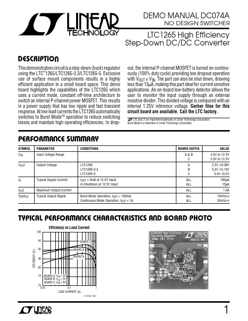
1SYMBOL PARAMETER CONDITIONSBOARD SUFFIXVALUE V IN Input Voltage Range A & B 3.5V to 12.5V C 5.0V to 12.5V V OUTOutput VoltageLTC1265A 2.5V ±0.06V LTC1265-3.3B 3.3V ±0.10V LTC1265-5C 5.0V ±0.2VI Q Typical Supply Current I OUT = 0mA at 12.5V Input ALL 160µA In Shutdown at 12.5V InputALL 15µA I OUT Maximum Output Current ALL 1.0A V RIPPLETypical Output RippleBurst Mode Operation, I OUT= 100mA ALL 70mV P-P Continuous Mode Operation, I OUT = 1A ALL30mVP-PStep-Down DC/DC ConverterDESCRIPTIOUThis demonstration circuit is a step-down (buck) regulator using the LTC ®1265/LTC1265-3.3/LTC1265-5. Exclusive use of surface mount components results in a highly efficient application in a small board space. This demo board highlights the capabilities of the LTC1265 which uses a current mode, constant off-time architecture to switch an internal P-channel power MOSFET. This results in a power supply that has low ripple and fast transient response. At low load currents the LTC1265 automatically switches to Burst Mode TM operation to reduce switching losses and maintain high operating efficiencies. In drop-out, the internal P-channel MOSFET is turned on continu-ously (100% duty cycle) providing low dropout operation with V OUT ≅ V IN . The part can also be shut down, drawing less than 15µA, making this part ideal for current sensitive applications. An on-board low-battery detector allows the user to monitor the input supply through an external resistive divider. This divided voltage is compared with an internal 1.25V reference voltage. Gerber files for this circuit board are available. Call the LTC factory.TYPICAL PERFOR A CE CHARACTERISTICS A D BOARD PHOTOU UW LOAD CURRENT (A)0.0170E F F I C I E N C Y (%)758085901000.11DC074A • TA0195Efficiency vs Load CurrentBurst Mode is a trademark of Linear Technology Corporation.PERFOR A CE SU ARYU W WW2DEMO MANUAL DC074ASYMBOL PARAMETERCONDITIONSBOARD SUFFIXVALUE ∆V OUTTypical Load Regulation0mA < I OUT < 1A, V IN = 10V A 30mV 0mA < I OUT < 1A, V IN = 10V B 50mV 0mA < I OUT < 1A, V IN = 10VC 70mV V IH Shutdown Pin High Minimum Voltage at Pin 10 for Device to Be in Shutdown ALL 1.2V V IL Shutdown Pin Low Maximum Voltage at Pin 10 for Device to Be in ActiveALL 0.6V I QLow-Battery Trip PointALL1.25 ±0.1VPERFOR A CE SU ARYU W WWS PACKAGE14-LEAD PLASTIC SOIC *ADJ OUTPUT VERSIONSPWR V IN V IN LB OUT LB IN C T I TH SENSE –SW PWR V IN PGND SGND SHDN NC (V FB *) SENSE +LTC1265CS LTC1265CS-3.3LTC1265CS-5V OUT µF LTC1265 LTC1265-3.3 LTC1265-5PACKAGE A D SCHE ATIC DIAGRA SU W WPARTS LISTREFERENCE DESIGNATOR QUANTITYPART NUMBER DESCRIPTIONVENDOR TELEPHONE C11VJ1206A392KXAT Cap, Mono Chip, 3900pF, 50V, 10%Vitramon (203) 268-6261C21VJ1206U103MXAT Cap, Mono Chip, 0.01µF, 25V, 10%Vitramon C31VJ1206U104MXXAT Cap, Mono Chip, 0.1µF, 25V, 10%Vitramon C41VJ1206A101KXAT Cap, Mono Chip, 100pF, 50V, 10%Vitramon C51VJ1206A181JXAT Cap, Mono Chip, 180pF, 50V, 5%: Board AVitramon VJ1206A151JXAT Cap, Mono Chip, 150pF, 50V, 5% : Board B & C C61593D686X0020E2W Tantalum Cap, 68µF, 20V, 20%Sprague (207) 324-4140C71593D107X0010D2W Tantalum Cap, 100µF, 10V, 20%Sprague D11MBRS130LT3Schottky DiodeMotorola (602) 244-3558L11LPT4545-200Inductor, 20µH : Board A & B Dale(605) 665-9301LPT4545-330Inductor, 33µH : Board CFigure 1.3DEMO MANUAL DC074APARTS LISTREFERENCE DESIGNATOR QUANTITY PART NUMBER DESCRIPTION VENDOR TELEPHONE R1 1WSL2010-0.10.1Ω 1% 0.5W Resistor Dale (605) 665-9301R2 1CRCW1206499J 499Ω 5% Chip Resistor Dale R3 1CRCW1206223J 22k 5% Chip Resistor Dale RFB1, RFB2 1CRCW1206343J 34k 5% Chip Resistor: Board A Dale U11LTC1265CS Board A IC LTC(408) 432-1900LTC1265CS-3.3Board B IC LTC1265CS-5Board C ICQUICK START GUIDEThis demonstration board is easy to set up to evaluate the performance of the LTC1265. Please follow the procedure outline below for proper operation.•Connect the input power supply to the V IN and GND terminals.•The LB OUT pin is a current sinking pin. When the LB IN pin goes below 1.25V the LB OUT pin will sink 1mA of current.•The LB IN pin is the low battery detector input pin.Normally, its input comes from the input voltagethrough a resistive divider network (see LOW BAT-TERY DETECTOR).•Connect the load between the V OUT and GND terminals.•Refer to Figure 4 for proper arrangement of measure-ment equipment setup•The SHDN pin is pulled down to ground by R3. To put the part in shutdown, connect a voltage greater than 1.2V to this pin.OPERATIOUcurrent limit and excellent line and load regulation. The constant off-time adds to this list simplicity (neither an oscillator nor ramp compensation are required), inherent 100% duty cycle in dropout, and constant inductor ripple current.Because the off-time is constant, the operating frequency changes with input voltage. For example, in an LTC1265-3.3 application the frequency will double when V IN is increased from 4.7V to 8V with V OUT at 3.3V. To maximize the efficiency over a wide current range, loss reducing circuit techniques must be carefully applied. Because of the MOSFET gate charge, switching the gate from V IN to ground ends up as additional input current from V IN ,decreasing efficiency. At low output currents this loss term dominates. This is the principal reason that the LTC1265 changes to Burst Mode operation as the output current drops.The circuit shown in Figure 1 operates from input voltages of 3.5V to 12.5V. For Board A, the output voltage is set to 2.5V by the resistive dividers, RFB1 and RFB2. For Board A and Board B, the circuit is optimized at input voltage of 5V while Board C is optimized at a 9V input voltage. For all boards, the LTC1265 is operating at a frequency of 200kHz when at their respective optimized input voltage and the LTC1265 is operating in continuous mode.This demonstration unit is intended for the evaluation of the LTC1265 switching regulator IC and was not designed for any other purposes.OPERATIONThe LTC1265 switching regulator uses the constant off-time, current mode architecture shown in Figure 2.Current mode operation was judged to be mandatory for its well-known advantages of clean start-up, accurate4DEMO MANUAL DC074AOPERATIOUThe continuous mode operation is as follows: the internal P-channel MOSFET switch is turned on at the end of the off-time and turned off when the inductor current has ramped up to the current comparator threshold. During the off-time the catch diode D1 turns on. At the end of the constant off-time, the P-channel MOSFET is again turned on and the cycle repeats.LTC1265 Burst Mode is automatically invoked when the current required by the load is less than the minimum current supplied by the continuous operation. During Burst Mode operation the output voltage is regulated via a hysteretic comparator which, when tripped, shuts down the MOSFET driver and much of the control circuitry to conserve DC supply current. From the time the compara-tor trips until the lower comparator threshold is reached,the load current is completely supplied by a charge stored in the output capacitor. When the output capacitor dis-charges to the lower threshold, the main loop again briefly turns on at a low current level to recharge the capacitor.This cycle repeats at a progressively slower rate as the output current is reduced.LOW-BATTERY DETECTORThe low-battery indicator senses the input voltage through an external resistive divider. This divided voltage connects to the (–) input of a voltage comparator (Pin 4) which is compared with a 1.25V reference voltage. With the current going into pin 4 being negligible, the following expression is used for setting the trip limit:V LB_TRIP = 1.251 +R4R3))Figure 2. LTC1265 Block DiagramFigure 3. Low-Battery ComparatorV FBADJUSTABLE VERSIONV DC074A • F035DEMO MANUAL DC074AOPERATIOUHOW TO MEASURE VOLTAGE REGULATIONWhen trying to measure voltage regulation remember that all measurements must be taken at the point of regulation. This point is where the LTC1265’s control loop looks for the information to keep the output voltage constant. This information occurs between Pin 7 and Pin 11 of the LTC1265. These points correspond to the output terminals of the demonstration board. Test leads should be attached to these terminals. Measurements should not be taken at the end of test leads at the load . Refer to Figure 4 for proper monitoring equipment configuration.This applies to line regulation (input to output voltage regulation) as well as load regulation tests. In doing line regulation tests always look at the input voltage across the input terminals.For the purposes of these tests the demonstration circuit should be fed from a regulated DC bench supply, so additional variation on the DC input does not add an error to the regulation measurements.The technique used to measure the ripple is also impor-tant. Here is a list of things to do and not to do when using a scope probe:1.DO NOT USE THE GROUND LEADS/CLIPS THAT ARE ATTACHED TO THE SCOPE PROBE!2.DO ATTACH THE SHIELD OF THE PROBE BODY TO THE NEGATIVE SIDE OF THE OUTPUT CAPACITOR!DO NOT USE WIRE!3.DO PUT THE TIP OF THE SCOPE PROBE DIRECTLY ON THE POSITIVE TERMINAL OF THE OUTPUT CAPACITOR.4.DO NOT USE A PROBE WHOSE BODY IS NOT COMPLETELY SHIELDED.Any unshielded lead, such as a ground lead on a scope probe, acts as an antenna for the switching noise in the supply. Therefore any use of a ground lead will invalidate the measurement.Be extremely careful to ensure that other sources of noise do not invalidate the measurement. Noise from the 60Hz power line that feeds the bench power supply poweringDC074A • F04RIPPLE MEASUREMENTFor the purpose of measuring output ripple it is best to measure directly across the output terminals.As in the regulation tests the supply must be fed from a regulated DC source so that ripple on the input to the circuit under test does not add to the output ripple,causing errors in the measurement.Figure 4. Proper Measurement Setupthe LTC1265 demonstration board can cause errors in the measurement. This noise (especially spikes) can propa-gate through the bench supply and appear on the groundFigure 5. Scope Probe and Typical Measurement SetupDEMO MANUAL DC074Aof the demonstration unit. If this is a problem, a battery canbe used to power the unit for ripple tests.Also be wary of ground loops. The input DC supply shouldfloat and the only ground should be that of the scopeprobe. Never float the oscilloscope as it may present asafety hazard.An alternate technique is to take a 50Ω or 75Ω piece ofcoax and solder the leads directly to the output capacitor.Keep the shield over the center conductor for as great adistance as possible. The center conductor can pick up stray radiation when it is not shielded, so minimize thelength of exposed center conductor. The other end of thecoax should have a BNC connector for attaching to theoscilloscope.CHECKING TRANSIENT RESPONSESwitching regulators take several cycles to respond to astep in DC (resistive) load current. When a load stepoccurs, V OUT shifts by an amount equal to ∆I LOAD× ESR, where ESR is the effective series resistance of C OUT.∆I LOAD also begins to charge or discharge C OUT until the regulator loop adapts to the current change and returnsV OUT to its steady-state value. During this recovery time V OUT can be monitored for overshoot or ringing which would indicate a stability problem. The external compo-nents shown in the Figure 1 circuit will prove adequate for most applications.A second, more severe transient is caused by switching inloads with large (>1µF) supply bypass capacitors. Thedischarged bypass capacitors are effectively put in parallelwith C OUT, causing a rapid drop in V OUT. No regulator can deliver enough current to prevent this problem if the load switch resistance is low and it is driven quickly. The only solution is to limit the rise time of the switch drive so that the load rise time is limited to approximately 25 × C LOAD. Thus a 10µF capacitor would require a 250µs rise time, limiting the charging current to about 200mA.COMPONENTSComponents selection can be very critical in switching power supply applications. This section discusses some of the guidelines with selecting the different components. The LTC1265 data sheet details more specific selection criteria for most of the external components surrounding the IC. Be sure to refer to the data sheet if changes to this demo circuit are anticipated.CapacitorsThe most common component uncertainty with switching power supplies involves capacitors. In this circuit (refer to Figure 1) C6 and C7 are all specially developed low ESR, high ripple-current tantalum capacitors specifically designed for use in switching power supplies. ESR or Equivalent Series Resistance is the parasitic series resis-tance in the capacitor. Very often this resistance is the limiting element in reducing ripple at the output or input of the supply. Standard wet electrolytics may cause the feedback loop to be unstable (this means your power supply becomes an oscillator). They may also cause poor transient response or have a limited operating life. Standard parts normally do not have an ESR specification at high frequencies (100kHz) so, although you may find a part that works to your satisfaction in a prototype, the same part may not work consistently in production. Furthermore, surface mount versions of wet electrolytics are not space efficient, and they may have high ESR and limited lifetimes.Normal tantalums are not recommended for use in these applications (most notably the low cost ones) as they do not have the ability to take the large peak currents that are required for the application. Tantalums have a failure mechanism whereby they become a low value resistance or short. Wet electrolytics rarely short; they usually fail by going high impedance if over-stressed. Very few tantalum manufacturers have the ability to make capacitors for power applications.There are some tantalums, such as those used in this design, that are specifically designed for switching power supplies. They are much smaller than wet electro-lytic capacitors and are surface mountable but they do cost more.One other choice that fits between wet electrolytics and tantalums is organic semiconductor type capacitors (OS-CON) that are specifically made for power supply applications. They are very low ESR and are ≈1/2 the size of an equivalent wet electrolytic.OPERATIOU67DEMO MANUAL DC074AInformation furnished by Linear Technology Corporation is believed to be accurate and reliable.However, no responsibility is assumed for its use. Linear Technology Corporation makes no represen-tation that the interconnection of its circuits as described herein will not infringe on existing patent rights.InductorTo most engineers, inductors are the least familiar compo-nent in a switching power supply. This is unfortunate because the most flexible component in the system is the inductor. The size, shape, efficiency, form factor and cost are variables that can be traded off against one another.The only fixed requirement of the inductor used with the LTC1265 is that it must be able to support the output DC current and still maintain its inductance value.Although the inductor used in the demo board is from Dale, there are a wide variety of inductors available from other manufacturers. Sumida’s CDR 74B, CD75, CDR105B and CDR125 series are suitable for this demo board.In addition, Coilcraft’s DO3316 series and Coiltronics CTX series are also suitable in this demo board. However,re-characterizing the circuit for efficiency is necessary if any of the alternate inductors are used in place of the existing one.There are many inductors that will work in this circuit. Each inductor design will have a different physical size, different loss characteristics as well as different stray field patterns.All of these items must be considered to optimize a design.Because of the aforementioned variations in design and cost of inductor, we suggest you contact some of the inductor manufacturers in Table 1 and discuss your needs with them. Very often, a standard low cost solution which will meet your needs is on the shelf.Sense ResistorThe current sense resistor specified in the component list is manufactured by Dale. Alternate resistor sources include International Resistive Company and the SL, SP series by KRL/Bantry.Schottky DiodeThe catch diode carries load current during the off-time.The average diode current is therefore dependent on the P-channel switch duty cycle. At high input voltages the diode conducts most of the time. As V IN approaches V OUT the diode conducts only a small fraction of the time. The most stressful condition for the diode is when the output is short-circuited. Under this condition the diode must safely handle I PEAK at close to 100% duty cycle. A fastOPERATIOUswitching diode must also be used to optimize efficiency.Schottky diodes are a good choice for low forward drop and fast switching times. Most LTC1265 circuits will be well served by a MBRS130LT3 Schottky ponent ManufacturersBesides those components that are used on the demon-stration board, other components may also be used.Below is a partial list of the manufacturers whose compo-nents you can use for the switching regulator. Using components, other than the ones on the demonstration board, requires re-characterizing the circuit for efficiency.Table 1. Inductor ManufacturerMANUFACTURER PART NUMBERS CoilcraftD03316 Series1102 Silver Lake Road Cary, Illinois(Phone) 708-639-6400(Fax) 708-639-1469Coiltronics InternationalEcono-Pac 6000 Park of Commerce Blvd.Octa-PacBoca Raton, FL 33487(Phone) 407-241-7876(Fax) 407-241-9339Dale Electronics Inc.LPT4545E. Highway 50P.O. Box 180Yankton, SD 57078-0180(Phone) 605-665-9301(Fax) 605-665-1627Sumida Electric Co. Ltd.CD 74B Series 5999 New Wilke Rd., Suite #110CD 75 Series Rolling Meadows, IL 60008CDR105B(Phone) 708-956-0666(Fax) 708-956-0702Table 2. Capacitor ManufacturersMANUFACTURER PART NUMBERS AVX Corporation TPS SeriesP.O. Box 887Myrtle Beach, S.C. 29578(Phone) 803-448-9411(Fax) 803-448-1943Sanyo Video Components OS-CON Series2001 Sanyo Avenue San Diego, CA 92071(Phone) 619-661-6322(Fax) 619-661-1055Sprague593D Series678 Main Street Sanford, ME 04073(Phone) 207-324-4140(Fax) 207-324-72238DEMO MANUAL DC074A Linear Technology Corporation1630 McCarthy Blvd., Milpitas, CA 95035-7487(408) 432-1900 qFAX : (408) 434-0507 qTELEX : 499-3977© PCB LAYOUT A D FIL WUComponent Side Solder MaskSolder Side Solder MaskPC FAB DRAWI GUSYMBOLA B DIAMETER 0.094 0.018 NUMBEROF HOLES7 4 11TOTAL HOLES DC074A • PCB01Component SideSolder SideComponent Side Silkscreen。
FLUKE123/124 使用手册

服务中心
欲安排一家授权的服务中心,请与我们在全球网(World Wide Web)上的地址联络:
1
测试仪的使用 ................................................................................................................. 7
本章的目的..................................................................................................................... 7 给测试接通电源.............................................................................................................. 7 将测试仪复位 ................................................................................................................. 8 改变背衬光..................................................................................................................... 9 视屏判读 ........................................................................................................................ 10 菜单的选择..................................................................................................................... 11 测量接口 ........................................................................................................................ 12 用连通和检视(Connect-and-View™)显示未知信号.................................................... 13 进行测量 ........................................................................................................................ 14 锁定视屏 ........................................................................................................................ 16
RPT1266型继电保护测试系统使用说明书.doc

TP—1200微机继电保护测试仪使用说明书武汉拓普特电力自动化有限公司ﻬ前言继电保护测试装置是保证电力系统安全可靠运行的一种重要测试工具。
随着现代电力系统规模的不断扩大,对电力系统运行和管理的可靠性、高效性要求的不断提高,继电保护人员的测试工作变得更加频繁和复杂。
在计算机技术、微电子技术、电力电子技术飞速发展的今天,应用最新技术成果不断推出新型高性能继电保护测试仪是技术进步的必然趋势,也是时代赋予我们的责任。
TP-1200微机继电保护测试仪是在参照中华人民共和国电力行业标准《继电保护微机型试验装置技术条件》(DL/T 624 ─1997)的基础上,广泛听取用户意见,总结目前国内同类产品优缺点,充分使用现代先进的微电子技术和器件实现的一种新型小型化微机继电保护测试仪.它采用可单机独立运行,亦可联接其它电脑运行的先进结构,主机内置高性能工控机和高速数字信号处理器,真16位DAC模块、新型模块式高保真大功率功放,自带TFT真彩色LCD显示器和嵌入式微机键盘。
既可以单机独立操作,也可以连接笔记本电脑操作.操作功能强大,体积小,精度高。
既具有大型测试仪优越的性能、先进的功能,又具有小型测试仪小巧灵活、操作简便、可靠性高等优点,性能价格比高。
是继保工作者得心应手的好工具.ﻬ目录第一章继电保护测试仪说明 (5)1.1主要技术特点 (5)1.2主要技术指标 (6)1.3面板说明 (9)1.4硬件结构………………………………………………………101.5仪器的操作使用 (11)1.6注意事项………………………………………………………13第二章继电保护测试仪使用方法.................................15 2.1递变试验×7 (15)2.2递变试验×12 ………………………………………………202.3状态序列 (24)2.4谐波试验 (27)2.5整组试验………………………………………………………322.6差动保护试验.........................................................37 2.7频率试验 (43)2.8同期试验 (46)2.9电流—时间特性试验…………………………………………49 2.10电压-时间特性试验…………………………………………522.11故障再现………………………………………………………552.12距离保护试验.........................................................642.13零序保护试验 (69)2.14阻抗特性试验 (73)附录1:试验方法.........................................................78附录2:差动保护知识 (87)附录3:配置清单 (9)1附录4:售后服务 (92)ﻬ第一章继电保护测试仪说明1.1 主要技术特点微机型继电保护测试仪其主要特点表现为:经典的Windows XP操作界面,人机界面友好,操作简便快捷,为了方便用户使用,定义了大量键盘快捷键,使得操作“一键到位”;●高性能的嵌入式工业控制计算机和8。
VC26H多功能过程校验仪说明书_中文(0.0)

多功能过程校验仪声明:本手册适用于HART型和基本型的多功能过程校验仪仪表。
与HART相关的操作仅适用于HART型。
手册内所有的解释和范例是以HART型型作说明的。
1引言多功能过程校验仪(以下简称校验仪)是一个由电池/适配器供电,能测量和输出电参数和物理参数的手持便携式仪器(见表1)。
表 1. 输出和测量功能一览表除表1所列的功能以外,校验仪还具有下列特性:▪任何功能状态都可直接进入HART功能(仅限HART型)。
▪测量和输出可同时工作。
测量信息与输出信息分屏显示。
▪热电偶(TC)输入/输出端子及校验仪内部具有自动参考节点温度补偿。
▪手动步进输出及自动步进和斜波电流输出。
▪任何操作下的室温监视▪测量/输出温度监视功能▪测量/输出mA%显示▪测量滤波功能▪测量手动保持功能▪压力输出显示值的自动保持功能2与我们联系欲订购部件、寻求操作上的协助或取得最靠近您的经销商或维修中心的地点,请打电话,或请探访公司网址:(见说明书封底)3标准配置以下所列的项目均包含在您的校验仪内,如果您发现校验仪有损坏或缺少一些东西,应立即与购买单位联系。
欲订购更换零件或备件,请参见本手册15.3所列的用户可更换的备件清单。
▪测试表笔(H000000-00) 1付▪工业测试导线(H000001-00) 1付▪工业测试导线(H000002-00) 1付▪钩式测试表笔(H000004-00) 1付▪鳄鱼夹(H010000-00) 1付▪鳄鱼夹(H010007-00) 1付▪热电偶转接头(H200000-00) 1个▪使用说明书 1本▪产品合格证明书 1份▪保险管(100mA/250V) 2只▪保险管(50mA/250V) 2只▪5号碱性电池 4节▪布包 1个4安全信息用户应按照本说明书的指示使用校验仪,否则校验仪所提供的保护措施可能会受到损坏。
对于没有按照所给的安全警示信息进行操”指出可能对用户构成危险的情况或行为;“小心”指出可能对校验仪或被测试设备造成损坏的情况或行为。
威尔海温控器产品说明书
温控器产品说明书深圳市威尔海电子有限公司电话:0755-2953 9385 传真:*************技术支持:田工①安装开口尺寸:②接线图:电源接线柱1和2 : 制冷输出接线柱1和3 : 化霜输出接线柱1和4: 风机输出接线柱5和6: 接电源接线柱7和8 接化霜温度传感器接线柱9和10: 接制冷温度传感器锁定开关: 将1或2拨到ON的位置,可将已经设定好的控制参数锁定。
指示灯状态说明:WORK指示灯为工作指示灯,闪烁表示制冷延时,长亮表示制冷工作。
SET指示灯为设置指示灯,长亮表示在设置状态。
..◆设定控制温度:在待机状态下按SET键一次进入控制温度设置,按▲或▼键调整,按住▲或▼键三秒不放进入快速调整模式.再按SET键一次回到待机状态.设置控制参数:按住SET键三秒不放进入控制参数设置,按▲或▼键选择要调整的菜单,再按SET键一次进入相应的控制参数设置状态,按▲或▼键调整需要修改的控制参数,调整好后按RST键退出,或系统延时5秒退出菜单代码说明:菜单代码详细说明 解释 单位D 回差 开机和停机之间的温度差℃LS 设置下限 控制温度可设定的最小值℃HS 设置上限 控制温度可设定的最大值℃CA 温度较正 ℃PT 延时启动 最小开停机时间间隔 分钟DC 化霜周期 小时DT 化霜时间 分钟DL 化霜滴水时间 分钟DE 化霜停止温度 ℃DP 化霜时显示设置 00:显示NTC1温度01:显示NTC2温度 FD 风机工作模式 00:与压缩机同启同停01:一直工作,化霜时除外制冷控制:当测量温度值≥控制温度+回差时,启动输出,继电器吸合;当测量温度<控制温度时,关闭输出,继电器断开。
设置举例: 控制温度为25度,回差设为5, 那么当测量温度低于25度时继电器断开,关闭输出.当温度高于或等于30度时再接通继电器,启动输出◆回差功能:回差设置限定了开机和停机之间的最大温度差。
◆回差设定:按"SET"键不放超过3秒,进入菜单显示,用“▲”或"▼"键调至屏幕出现"D"代码时,按"SET" 键显示回差设定值,再按“▲”或"▼"键调整参数.◆温度校正功能:当测量温度与标准温度有偏差时,可使用温度校正功能,使机器的测量值与标准温度一致,校正后的温度=校正前的温度值+校正值(校正值可以为正数、负数和0)。
Omron LC2H数字计数器产品说明书
Product types1. Panel mounting type1) One-touch installation typePanel mounting type One-touch installation typePanel mounting type Installation frame typePC board mounting typeFeatures1. 8.7 mm .343 inch Character Height (previously 7 mm)Easy-to-read character height increased from 7 mm to 8.7 mm .276 inch to .343 inch .2. Plenty of Digits3. Counting Speed Switchable between 2 kHz and 30 Hz4. Panel Mounting Type Features2 Installation MethodsComes with very easy one-touch installation type and also installation frame type that uses the bracket on the timer/counter. Choose a method that suits the application.5. Battery Replacement Easy on EnvironmentT o replace battery simply remove body for the one-touch installation type, and remove battery lid for the installation frame type.6. Screw Terminals Designed for SafetyBuilt in finger protection.7. Panel Covers Replacable (Standard color is ash gray.)Change the panel design by replacing with a black panel cover.8. Conforms to IP66 ProtectiveConstruction (Only installation frame type.) (Front panel surface)9. Input Methods1) Non-voltage input method 2) Voltage input method3) Free voltage input method10. Backlight Type Added to Series and Now 2-color Switchable (green/red)Easy viewing even in dark places and switchable between green and red (Voltage input type).11. Compliant with UL, c-UL and CE.RoHS Directive compatibility information/Product chart2) Installation frame typeSpecificationsNotes)1.The value given for battery life is calculated based on continuous operation (count input signal ON/OFF = 1:1), therefore, this value is not guaranteed.Also, battery life is decreased 30% when operation is continuous with 2 kHz count inputting in 2 kHz mode.2.Operation is at 25 Hz when using 24 V AC.3.Only for installation frame type.Applicable standardPart names1. Front reset buttonThis button resets the count value. It does not work when the lock switch is ON. Be aware that battery life willdecrease if this switch is used frequently.2. Lock switch (Refer to chart on right.)Disable the front reset button.Note)T urn ON at the LCD side (reset disabled) andOFF at the terminal block side (reset enabled).3. Count speed switch (Refer to chart on right.)Use this switch to switch the count speed between 30 Hz and 2 kHz. (On the non-voltage and voltage input types, 30 Hz is on the LCD side and 2 kHz is on the terminal block side. Fixed at 30 Hz for free voltage input type.)Note)Y ou must press the front reset button when youchange the count speed switch setting.Confirm, however, that the Lock Switch is OFF (front switches operable).Notes)1.❇Default setting when shipped.2.Make the switch setting before installing to panel.Dimensions1. Panel mounting type • External dimensions1) One-touch installation typemm inchGeneral tolerance: ±1.0 ±.039• Panel installation diagramNote)When installing to a 4.5 mm .177 inch thick panel, remove the rubber spacerfirst.When installing the one-touch installation type model, make sure that the installation spring does not pinch the rubber gasket.T o prevent the installation spring from pinching the rubber gasket:1. Set the rubber gasket on both ends of the installation spring (left and right).2. Confirm that the installation spring is not pinching the rubber gasket, and then insert and fix the installation spring in place from therear of the timer unit.• Terminal layout and wiring diagrams2) Installation frame type• Panel mounting diagramMounting screwsMounting frame • Panel cut-out dimensionsThe standard panel cut-out is shown below.Use the mounting frame (ATH3803) and the rubber packing (ATH3804).(Only installation frame type.)• For connected installation (sealed installation) (Only installation frame type.)Notes)1. Suitable installation panel thickness is 1 to 4.5 mm .039 to .177 inch .2. Waterproofing will be lost when installing repeatedly (sealed installation).A=(1.890×n-.098)0+.0390Input methodNotes)1.2 and 4. (The input and reset circuits are functionally insulated.)2.When using transistor (T r) input, use the right as a guide. (Collector withstand voltage Q 50 V , leakage current < 1 µA)3.Be aware that the application of voltage that exceeds the voltage range of the H level to the count input terminal, and the application of voltage to the reset input terminal, can cause damage to the internal elements.2. PC board mounting type • External dimensions• Terminal layout and wiring diagramsGeneral tolerance: ±1.0 ±.039 mm inchPC board pattern (BOTTOM VIEW)General tolerance: ±0.1 ±.004Note: The AXS212811K is recommended as a compatible connection socket.0.3.012±.004Q -E , }-w , e -t and S -F are connected internally.An external power supply is required.Connection sockets 28 pin DIP terminalNotes)1.Do not reverse the polarities when connecting the DC voltage for the backlight.2.2 and 4. (The input and reset circuits are functionally insulated.)3.When using transistor (T r) input, use the right as a guide. (Collector withstand voltage Q 50 V , leakage current < 1 µA)4.Be aware that the application of voltage that exceeds the voltage range of the H level to the count input terminal, and the application of voltage to the reset input terminal, can cause damage to the internal elements.Explanation of operation1. Counting takes place when the count input signal is ON.2. Counting resumes again when the count value reaches 99999999 (full scale value) and then returns to “0” with a new count input.3. No measurement takes place when a reset is input.1) When reset is ON, resetting takes place and the count becomes “0”.2) Press the front reset button when you want to reset manually (only panel installation type).Note)Be aware that battery life will decrease if thecount input or reset input are left ON.Note) ❇Count becomes “1” when the reset input is turned OFF while the count signal is being input.Cautions for use1. Non-voltage input typeFor both panel mounting and PC board mounting types1) Never apply voltage to the non-voltage input type. This will damage the internal elements. Also, since there is a possibility of erroneous operation, do not connect in parallel the inputs of a non-voltage input type and another counter from a single input signal.2) Since the current flow is very small from the count input and reset input terminals (1 and 3 on the panel mounting type and terminals e to t and S to F on the PC board mounting type) please use relays and switches with high contact reliability.3) When inputting with an open collector of a transistor, use a transistor for small signals in which ICBO is 1 µA or less and always input with no voltage.4) When wiring, try to keep all the input lines to the count and reset inputs as short as possible and avoid running them together with high voltage and power transmission lines or in a power conduit. Also, malfunctions might occur if thefloating capacitance of these wires exceeds 500 pF (10 m 32.808 ft. for parallel wires of 2 mm2). When using 2 kHz mode, use with a wiring floating capacitance of 120 pF (3 m 9.843 ft. for parallel wires of 2 mm2). In particular, when using shielded wiring, be careful of the capacitance between wires.PC board mounting type1) For external power supply use manganese dioxide or lithium batteries (CR type: 3V).2) Always reset after external power is applied and confirm that the display reads “0”.3) Make the wiring from the battery to the counter unit as short as absolutely possible. Also, be careful of polarity.4) Calculate battery life with the following formula.t = A/It: battery life [h]I: LC2H current consumption [mA]A: battery capacity until minimumoperation voltage is reached [mAh] 5) Hand solder to the lead terminal. Do not dip solder. With the tip of the soldering iron at 300°C 572°F perform soldering within 3 seconds (for 30 to 60 W soldering iron).2. Voltage input type1) Be aware that applying more than 30 V DC to count input terminals 1 and 2, and reset input terminals 3 and 4 will cause damage to the internal elements.2) For external resetting use H level(application of 4.5 to 30 V DC) betweenreset terminals 3 and 4 of the rearterminals. In this case, connect + toterminal 3 and – to terminal 4. This isthe valid polarity; therefore, the counterwill not work if reversed.3) When wiring, try to keep all the inputlines to the count and reset inputs asshort as possible and avoid running themtogether with high voltage and powertransmission lines or in a power conduit.Also, malfunctions might occur if thefloating capacitance of these wiresexceeds 500 pF (10 m 32.808 ft. forparallel wires of 2 mm2).3. Free voltage input type1) Use count input terminals 1 and 2 forfree voltage input and reset terminals 3and 4 for non-voltage input.2) Be aware that the application ofvoltage that exceeds the voltage range ofthe H level to the count input terminal,and the application of voltage to the resetinput terminal, can cause damage to theinternal elements.3) Since the current flow is very smallfrom reset input terminal 3, please userelays and switches with high contactreliability.4) When inputting a reset with an opencollector of a transistor, use a transistorfor small signals in which ICBO is 1 µA orless and always input with no voltage.5) T o reset externally, short reset inputterminals 3 and 4 on the rear.6) Input uses a high impedance circuit;therefore, erroneous operation may occurif the influence of induction voltage ispresent. If you plan to use wiring for theinput signal that is 10 m or longer (wirecapacitance 120 pF/m at normaltemperature), we recommend the use ofa CR filter or the connection of a bleederresistor.4. How to reset multiple panelmounting type counters all at once(input is the same for count)Non-voltage input typeNotes)e the following as a guide for choosingtransistors used for input (Tr).Leakage current < 1 µAe as small a diode (D) as possible in theforward voltage so that the voltage betweenterminals 3 and 4 during reset input meetsthe standard value (0.5 V).( At IF = 20 µA, forward voltage 0.1 andhigher.)Voltage input typeNote)Make sure that H (reset ON) level is at least 4.5V.5. Backlight luminanceT o prevent varying luminance amongbacklights when using multiple Backlighttypes, please use the same backlightpower supply.6. Environment for use1) Ambient conditions• Overvoltage category II, pollution level 2• Indoor use• Acceptable temperature and humidityrange: –10 to +55°C, 35 to 85%RH (withno condensation at 20°C)• Under 2000 m elevation2) Use the main unit in a location thatmatches the following conditions.• There is minimal dust and no corrosivegas.• There is no combustible or explosivegas.• There is no mechanical vibration orimpacts.• There is no exposure to direct sunlight.• Located away from large-volumeelectromagnetic switches and powerlines with large electrical currents.3) Connect a breaker that conforms toEN60947-1 or EN60947-3 to the voltageinput section.4) Applied voltage should be protectedwith an overcurrent protection device(example: T 1A, 250 V AC time lag fuse)that conforms to the EN/IEC standards.(Free voltage input type)。
tpc-h教师实验指导书
TPC-H通用微机接口实验系统教师用实验指导书清华同方教学仪器设备公司2002年11月目录一、概述 (65)二、安装 (66)三、实验台结构:(见上页) (62)1、I/O地址译码电路 (62)2、总线插孔 (62)3、时钟电路 (62)4、逻辑电平开关电路 (62)5、LED显示电路 (63)6、七段数码管显示电路 (63)7、单脉冲电路 (64)8、逻辑笔 (64)9、继电器及驱动电路 (64)10、复位电路 (64)11、接口集成电路 (65)12、跳线开关(JP) (65)13、+5V电源插针 (65)14、通用集成电路插座 (65)15、数字电路实验区 (65)16、接线端子 (65)17、50线总线插座信号安排 (66)18、直流电源开关(K1)和存储器地址选择开关(K2) (66)19、使用外加直流电源注意事项: (66)四、接口实验部分: (67)实验一 I/O地址译码 (67)实验二简单并行接口 (68)实验三可编程定时器/计数器 (71)实验四、可编程并行接口(一) (73)实验五七段数码管 (75)实验六继电器控制 (78)实验七竞赛抢答器 (81)实验八交通灯控制实验 (83)实验九中断 (85)实验十可编程并行接口(二) (88)实验十一数/模转换器 (91)实验十二模/数转换器 (94)实验十三数字录音机 (97)实验十四串行通讯 (101)实验十五DMA传送 (104)实验十六集成电路测试 (107)实验十七电子琴 (110)实验十八 8250串行通讯实验 (113)实验十九步进电机控制实验 (116)实验二十小直流电机转速控制实验 (120)实验二十一键盘显示控制器实验 (123)实验二十二存储器读写实验 (137)一、概述八十年代以来,国内大中专院校很多专业都相继开设了“微机原理及应用”方面的课程,讲授内容主要是8位机(Z80),实验设备多采用TP801单板机。
LCM1-1262A LoRaWAN 终端模块说明书
LCM1-1262A LoRaWAN终端模块说明书V2.2 LCM1-1262A LoRaWAN终端模块说明书版本V2.2LCM1-1262A LoRaWAN终端模块说明书V2.2一、产品说明LoRa联盟是2015年3月Semtech牵头成立的开放的、非盈利的组织.联盟发布一个基于开源的MAC层协议的低功耗广域网。
标准:LoRaWAN协议标准。
网络拓扑:星形结构。
网络构成:LoRa模块、网关(Gateway或称基站)、Server(包括Network Server,Network control,Application Server)。
LoRaWAN把LoRa模块分为A/B/C三类.、本产品使用SX1262作为射频芯片,搭建一款低功耗单片机来实现LORAWAN来进行数据的收发操作。
本产品支持全频段,315M、470M、868M、915M。
1.1技术参数类别指标名称无线模块无线射频调制方式LoRaTM扩频频率范围150-960MHz发射功率5dBm~22dBm接收灵敏度-148dBm(SF=12,BW=10.4K)传输速率扩频因子(SF)和带宽(BW)设置传输距离4000-6000米天线连接外置SMA天线、弹簧天线数据接口数据接口TTL电平串口信号TxD,RxD串口速率1200~115200bps 串口校验None,Even,Odd 数据位8LoRaWAN支持模式Class A/Class C功耗输入电压 3.3V最大发射电流≤105mA(20dBm)最大接收电流<5mA休眠电流<1.5uA工作环境工作温度-40℃~85℃外观尺寸长*宽*高38*20*4(mm)LCM1-1262A LoRaWAN终端模块说明书V2.2 1.2模块尺寸图1.3模块引脚定义无线数传模块提供了大量的外部接口供给客户进行二次开发,如只使用串口进行透传,可只保留所需对应焊盘,方便用户封装和使用,具体的引脚如下表:标识功能备注1VCC 3.3V2GND电源地3RXD串口接收口,接用户TX4TXD串口发送口,接客户RX5SWIM MCU芯片程序烧入,可做二次开发6RST复位脚,低电平复位7VCC 3.3V8GND电源地LCM1-1262A LoRaWAN终端模块说明书V2.29~20 24~31I/O足够的包括SPI,UART,ADC等各类功能接口,帮助进行二次开发,如有需要请联系21GND模块地22ANT天线23GND模块地二、LoRaWAN模式介绍LoRaWAN分成3种工作模式,分别为Class A,Class B,Class C2.1Class A模式主要用于定时主动上报,平时处理休眠状态,需要上报数据时,才会起动发送机制。