曼码编码-译码芯片3d7523
基于AVR单片机的曼彻斯特编解码及其应用_王建国
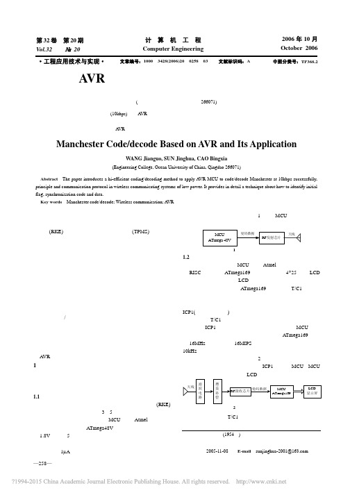
—258— 基于A VR 单片机的曼彻斯特编解码及其应用王建国,孙敬华,曹丙霞(中国海洋大学工程学院,青岛 266071)摘 要:提出了一种在较高通信速率(10kbps)下用A VR 单片机软件实现曼彻斯特码编解码的方法。
介绍了小功率无线传输系统的工作原理和通信协议。
详细阐述了用软件识别同步时钟、起始符、同步头和数据的技术方法。
关键词:曼彻斯特编解码;无线通信;A VR 单片机Manchester Code/decode Based on A VR and Its ApplicationWANG Jianguo, SUN Jinghua, CAO Bingxia(Engineering College, Ocean University of China, Qingdao 266071)【Abstract 】The paper introduces a hi-efficient coding/decoding method to apply A VR MCU to code/decode Manchester at 10kbps successfully,principle and communication protocol in wireless communicating systems of low power. It provides in detail a technique about how to identify initial flag, synchronization code and data.【Key words 】Manchester code/decode; Wireless communication; A VR计 算 机 工 程Computer Engineering 第32卷 第20期Vol.32 № 20 2006年10月October 2006·工程应用技术与实现·文章编号:1000—3428(2006)20—0258—03文献标识码:A 中图分类号:TP368.2随着无线通信芯片技术的发展,越来越多的便携式或电池供电的无线传输设备进入人们日常生活中。
曼彻斯特编码和解码的FPGA电路设计

Keyword: ManchesterCodeDifferentialManchester CodeFPGA
第一章
1.1
曼彻斯特编码是一种自同步的编码方式,也就是说其时钟同步信号就隐藏在数据波形中。在曼彻斯特编码中,每一位的中间有一跳变,位中间的跳变既作为时钟信号,又作为数据信号:从高电平到低电平的跳变表示“0”,从低电平到高电平的跳变表示“1”。还有一种是差分曼彻斯特编码,每位中间的跳变仅仅提供时钟定时,而用每位开始时有跳变为“0”,无跳变为“1”。由于曼彻斯特码既能提供足够的定时分量,又无直流漂移,编码过程相对简单,因而曼彻斯特码被广泛应用于数据传输、局域网以及测井技术等领域。本课题设计了一种利用曼彻斯特编码实现数据传输的通信系统。本文的主要工作就是研究曼彻斯特编解码器及差分曼彻斯特编解码器的设计及实现。
2.2
曼彻斯特码是通过电平的跳变来对二进制数据“0”和“1”进行编码的,对于何种电平跳变对应何种数据,实际上有两种不同的数据约定:第一种约定是由G. E. Thomas,Andrew S. Tanenbaum等人在1949年提出的,它规定“0”是由低到高的电平跳变表示,“1”是由高到低的电平跳变;第二种约定则是在IEEE 802.4(令牌总线)以及IEEE 802.3(以太网)中规定,按照这样的说法,由低到高的电平跳变表示“1”,由高到低的电平跳变表示“0”。在实际工程上,这两种约定在一定范围内均有应用。为了便于描述,若无特殊说明,本篇论文中的曼彻斯特码的编码规则均采用第二种约定,即从低电平跳变到高电平表示“1”,从高电平跳变到低电平表示“0”。
学习型编解码芯片组成的遥控装置

1.3 由eV1527和TDH6300组成的卷帘门遥控电路 1、电路组成 发射电路:
由控制指令按键K1、K2、二极管VD1、VD2、编码芯片 Ev1527和无线发射模块F05B组成。电阻R1=680Ω,电容 C1=0.1μF,R1和C1组成电源滤波电路。R2为芯片振荡电路 外接电阻,电源为VCC=9V的电池。
到的密码与存储器内的密码进行核对,因为已经过编码学习, TDH6300芯片内部存储器存有eV1527的密码,于是解码芯 片将解码后的控制指令送数据输出端8~11脚,8、9脚电平 依次为1和0,10及11脚没有使用。可见,控制指令成功地 通过无线收发电路从eV1527的8、7脚传输到TDH6300的8、 9脚。
工作电压:3~13V 待机电流:1μA 工作电流:0.5mA 芯片工作频率:80kHz 解码芯片TDH6300主要电学参数如下 工作电压:2~5.5V 待机电流:<3μA
1.2 编码学习的电路和操作步骤 1、编码学习的电路 编码芯片eV1527和解码芯片TDH6300组成的遥控电路包 电路, 也是正常工作时的遥控电路。发射电路如下
四个按键用来发出控制指令(例如控制汽车左转、右转、前 进、后退等)。
1.2 编码学习的电路和操作步骤 1、编码学习的电路 接收方电路如下图所示
无线接收模块解调后的信号经TDH6300的13脚进入解码芯片 进行密码识别并对控制指令进行解码。编码学习时,解码所得 密码将被存入TDH6300片内的E2PROM存储器内。
1.3 由eV1527和TDH6300组成的卷帘门遥控电路 1、电路组成 接收电路由无线接收模块J05C、解码芯片TDH6300、学习 按键K3和执行电路组成。
执行电路由继电器J1、J2、三极管VT1、VT2、发光二极管 VD3及单相交流电机组成。J1、J2均为一常开一常闭触点的继 电器,J1-1和J1-2分别为继电器J1的常开及常闭触点,J2-1和J2-2 分别为继电器J2的常开及常闭触点。
ADI ADAU1777音频编译码器(CODEC)数字处理方案

ADAU1777是一种具有四个输入和两个输出的编解码器,其包含数字处理引擎,用于执行滤波,电平控制,信号电平监视和混频。
从模拟输入到DSP内核到模拟输出的路径都针对低延迟进行了优化,是消除耳机噪声的理想选择。
虽然只启动几个无源元件,晶振和EEPROM,ADAU1777却提供了一个完整的耳机解决方案。
ADAU1777主要特性•可编程音频处理引擎•快速(高达768kHz)和慢速处理路径•Biquad过滤器,限制器,音量控制和混音•低延迟,24位ADC和DAC•102dB SNR(通过带有A加权滤波器的PGA和ADC)•108dB组合SNR(通过DAC和带A加权滤波器的耳机)•串口采样率从8kHz~192kHz•5μs模拟到模拟延迟•4个单端模拟输入,可配置为麦克风或线路输入•双立体声数字麦克风输入•立体声模拟音频输出,单端或差分,可配置为线路输出或耳机驱动器•PLL支持8MHz~27MHz的任何输入时钟速率•全双工,异步采样率转换器(ASRC)•电源•1.8V~3.3V模拟和数字输入/输出•数字信号处理(DSP)核心1.1V~1.8V•低电量•I2C和SPI控制接口,可从I2C EEPROM自启动•7个多用途(MPx)引脚,用于数字控制和输出ADAU1777应用•降噪手持设备,耳机和耳脉•蓝牙主动降噪(ANC)手持设备,耳机和耳脉•个人导航设备•数码相机和摄像机图1 ADAU1777功能框图ADI ADAU1777音频编译码器(CODEC)数字处理方案评估板EVAL-ADAU1777Z该评估板可完全访问ADAU1777上的所有模拟和数字输入/输出。
ADAU1777内核由ADI 公司的SigmaStudio 软件控制,该软件通过USB 连接与电路板连接。
EVAL-ADAU1777Z 可以由单个AAA 电池,USB 总线或单个3.8V~5.5V 电源供电; 任何这些电源都可调节到电路板上所需的电压。
印刷电路板(PCB )采用4层设计,在内层上具有单个接地平面和单个电源平面。
一种节省PLC输出口的编码译码方法

一种节省PLC输出口的编码译码方法
干耀国;杨前明
【期刊名称】《机电工程》
【年(卷),期】1994(000)004
【摘要】本文介绍了一种采用软件编码硬件译码的方法,达到节省可编程序控制器(PLC)用于设备运行状态显示输出口的目的。
【总页数】2页(P44-45)
【作者】干耀国;杨前明
【作者单位】不详;不详
【正文语种】中文
【中图分类】TM571.61
【相关文献】
1.一种新型光电轴角编码器译码方法研究 [J], 陈兴林;刘杨;吕恒毅
2.基于编码译码的PLC控制器输出口节能方法研究 [J], 张建根
3.微机实现光学全息编码和译码的一种新方法 [J], 柏永林;王冰
4.关于卷积码编码和译码的一种新方法 [J], 姚尹雄
5.一种节省PLCI/O点数的编码选控方法 [J], 汪雄海;嵇建飞;张利华;方晓琴
因版权原因,仅展示原文概要,查看原文内容请购买。
移运通信中迭代译码及其相关技术的研究和应用

移运通信中迭代译码及其相关技术的研究和应用
一. 引言
1.1 任务背景
1.2 任务目标
二. 迭代译码的基本概念和原理
2.1 译码的定义
2.2 迭代译码的概念
2.3 迭代译码的基本原理
三. 迭代译码的相关技术
3.1 Turbo码
3.1.1 Turbo码的基本原理
3.1.2 Turbo码的译码算法
3.2 低密度奇偶校验码(LDPC码)
3.2.1 LDPC码的原理
3.2.2 LDPC码的译码算法
四. 迭代译码的优势和应用
4.1 优势
4.2 应用领域
4.2.1 无线通信系统
4.2.2 光纤通信系统
4.2.3 卫星通信系统
五. 迭代译码技术的研究进展
5.1 迭代译码的改进方法
5.2 迭代译码算法的优化
5.3 迭代译码技术的未来发展方向
六. 结论
6.1 总结迭代译码的研究和应用
6.2 展望迭代译码技术的未来发展
七. 致谢
参考文献:(参考文献顺序列表)
注意:以上为示例,实际写作时需更具题目要求进行创作。
turbo码迭代译码
turbo码迭代译码Turbo码迭代译码引言:在现代通信系统中,为了提高通信系统的可靠性和传输速率,译码技术起着至关重要的作用。
Turbo码作为一种强大的编码和译码技术,被广泛应用于无线通信、卫星通信、数字电视等领域。
本文将重点介绍Turbo码的迭代译码原理及其应用。
一、Turbo码的基本原理Turbo码是一种串扰译码技术,它利用了两个编码器和一个交织器构成的编码器结构。
Turbo码的编码过程是将待发送的信息分别经过两个编码器,然后通过交织器进行交织,最终输出编码后的信号。
Turbo码的解码过程是一种迭代译码算法,通过将接收到的码字经过一个迭代译码器,然后再次通过交织器交织,最终得到译码后的信息。
二、Turbo码迭代译码原理Turbo码的迭代译码原理是基于迭代译码算法的。
迭代译码算法主要分为两个步骤:译码和交织。
在译码步骤中,输入接收到的码字,经过一次迭代译码器的译码过程,得到译码后的输出,然后将该输出通过交织器交织。
在交织步骤中,将交织后的输出输入到第二个迭代译码器进行译码,再次得到译码后的输出,然后再次通过交织器交织。
经过多次迭代,直到满足译码器的停止准则,得到最终的译码结果。
三、Turbo码迭代译码的优势Turbo码迭代译码相比于传统的译码算法具有以下优势:1. 更好的纠错性能:Turbo码迭代译码通过多次迭代,可以显著提高译码的纠错性能。
相比于传统的译码算法,Turbo码迭代译码可以在高信噪比下实现接近信道容量的性能。
2. 更低的译码延迟:Turbo码迭代译码的译码延迟相对较低,可以满足实时通信系统的要求。
3. 更好的抗干扰性能:Turbo码迭代译码通过迭代译码算法的优化,可以提高系统对多径衰落、多用户干扰等干扰源的抗干扰性能。
四、Turbo码迭代译码的应用Turbo码迭代译码广泛应用于无线通信、卫星通信、数字电视等领域。
在无线通信领域,Turbo码迭代译码被用于增强移动通信系统的抗干扰性能和提高系统容量;在卫星通信领域,Turbo码迭代译码被用于提高卫星通信系统的可靠性和传输速率;在数字电视领域,Turbo码迭代译码被用于提高数字电视信号的接收质量和抗干扰性能。
在各个领域中常用芯片汇总 (2)

在各个领域中常用芯片汇总1.音频pcm编码DA转换芯片cirrus logic的cs4344,cs4334,4334是老封装,据说已经停产,4344封装比较小,非常好用。
还有菲利谱的8211等。
2.音频放大芯片4558,833,此二芯片都是双运放。
为什么不用324等运放个人觉得应该是对音频的频率响应比较好。
3.74HC244和245,由于244是单向a=b的所以只是单向驱动。
而245是用于数据总线等双向驱动选择。
同时245的封装走线非常适合数据总线,它按照顺序d7-d0。
4.373和374,地址锁存器,一个电平触发,一个沿触发。
373用在单片机p0地址锁存,当然是扩展外部ram的时候用到62256。
374有时候也用在锁数码管内容显示。
5.max232和max202,有些为了节约成本就用max202,主要是驱动能力的限制。
6.网络接口变压器。
需要注意差分信号的等长和尽量短的规则。
7.amd29系列的flash,有bottom型和top型,主要区别是loader区域设置在哪里?bottom型的在开始地址空间,top型号的在末尾地址空间,我感觉有点反,但实际就是这么命名的。
8.164,它是一个串并转换芯片,可以把串行信号变为并行信号,控制数码管显示可以用到。
9.sdram,ddrram,在设计时候通常会在数据地址总线上加22,33的电阻,据说是为了阻抗匹配,对于这点我理论基础学到过,但实际上没什么深刻理解。
10.网卡控制芯片ax88796,rtl8019as,dm9000ae当然这些都是用在isa总线上的。
11.24位AD:CS5532,LPC2413效果还可以12.仪表运放:ITL114,不过据说功耗有点大13.音频功放:一般用LM36814.音量控制IC. PT2257/9.15.PCM双向解/编码 ADC/DAC CW6691.16.2.4G双工通讯 RF IC CC250017.24位AD:CS5532,LPC2413效果还可以18.仪表运放:ITL114,不过据说功耗有点大19.音频功放:一般用LM36820.音量控制IC. PT2257/9.21.PCM双向解/编码 ADC/DAC CW6691.cat809,max809,这些是电源监控芯片,当低于某一电压以后比如 3.07v等出现一个100ms的低电平,实现复位功能。
- 1、下载文档前请自行甄别文档内容的完整性,平台不提供额外的编辑、内容补充、找答案等附加服务。
- 2、"仅部分预览"的文档,不可在线预览部分如存在完整性等问题,可反馈申请退款(可完整预览的文档不适用该条件!)。
- 3、如文档侵犯您的权益,请联系客服反馈,我们会尽快为您处理(人工客服工作时间:9:00-18:30)。
datadelay devices, inc.3FEATURESPACKAGES• All-silicon, low-power CMOS technology• Encoder and decoder function independently • Encoder has buffered clock output• TTL/CMOS compatible inputs and outputs • Vapor phase, IR and wave solderable • Low ground bounce noise• Maximum data rate: 50 MBaud • Data rate range: ±15% • Lock-in time: 1 bit1413 12 11 10 9 1 2 3 4 5 6 CI CEN COUT DIN RESB VDD CBUF LOOP TXENB DOUTB TXB 3D7523D-xxx SOIC (.150)N RX 87GNDTXFUNCTIONAL DESCRIPTIONPIN DESCRIPTIONSEncoder:CIN Clock Input DIN Data Input RESB Reset CEN Clock buffer enable TXENB Transmit enable CBUF Buffered clock TX,TXB Transmitted signalDecoder: RX Received Signal COUT Recovered Clock DOUTB Recovered DataCommon:LOOP Loop enableVDD +5 VoltsGND GroundThe 3D7523 is a monolithic CMOS Manchester Encoder/Decoder combo chip. The device uses bi-phase-level encoding to embed a clock signal into a data stream for transmission across a communications link. In this encoding mode, a logic one is represented by a high-to-low transition in the center of the bit cell, while a logic zero is represented by a low-to-high transition.The Manchester encoder combines the clock (CIN) and data (DIN) into a single bi-phase-level signal (TX). An inverted version of this signal (TXB) is also available. The data baud rate (in MBaud) is equal to the input clockfrequency (in MHz). A replica of the clock input is also available (CBUF).The encoder may be reset by setting the RESB input low; otherwise, it should be left high. The TX and TXB signals may be disabled (high-Z) bysetting TXENB high. Similarly, CBUF may be disabled by setting CEN low.Under most operating conditions, TX and TXB are always enabled, andCBUF is not used. With this in mind, the 3D7523 provides internal pull-down resistors on CEN and TXENB, so that most users can leave these inputs uncommitted.The Manchester decoder accepts the embedded-clock signal at the RX input. The recovered clock anddata signals are presented on COUT and DOUTB, respectively, with the data signal inverted. Theoperating baud rate (in MBaud) is specified by the dash number of the device. The input baud rate may vary by as much as ±15% from the nominal device baud rate without compromising the integrity of the information received.Because the decoder is not PLL-based, it does not require a long preamble in order to lock onto thereceived signal. Rather, the device requires at most one bit cell before the data presented at the output is valid. This is extremely useful in cases where the information arrives in bursts and the input is otherwise turned off.Normally, the encoder and decoder function independently. However, if the LOOP input is set high, the encoded TX signal is fed back internally into the decoder and the RX input is ignored. This feature is useful for diagnostics. The LOOP input has an internal pull-down resistor and may be left uncommitted if this feature is not needed. 2007 Data Delay DevicesTABLE 1: PART NUMBER SPECIFICATIONSPART DECODER BAUD RATE (MBaud) NUMBER Nominal Minimum Maximum3D7523D-0.5 0.50 0.43 0.57 3D7523D-1 1.00 0.85 1.15 3D7523D-5 5.00 4.25 5.75 3D7523D-10 10.00 8.50 11.50 3D7523D-20 20.00 17.00 23.00 3D7523D-25 25.00 21.25 28.75 3D7523D-50 50.00 42.50 57.50NOTE:Any baud rate between 0.5 and 50 MBaud not shown is also available at no extra cost.APPLICATION NOTESENCODERThe encoder presents at its outputs the true and the complimented encoded data. The High-to-Low time skew of the selected data output should be budgeted by the user, as it relates to his application, to satisfactorily estimate thedistortion of the transmitted data stream. Such an estimate is very useful in determining the The Manchester encoder subsystem samples the data input at the rising edge of the input clock. The sampled data is used in conjunction with the clock rising and falling edges to generate the by-phase level Manchester code.The encoder employs the timing of the clockrising and falling edges (duty cycle) to implement the required coding scheme, as shown in Figure 1. To reduce the difference between the output data high time and low time, it is essential that the deviation of the input clock duty cycle from 50/50 be minimized.functionality and margins of the data link, if a Manchester decoder is used to decode the received data.RESET (RESB)CLOCK (CIN)DATA (DIN)(TX)(TXB)Figure 1: Timing Diagram (Encoder)(Left high for normal operation)APPLICATION NOTES (CONT’D)DECODERto one over twice the baud rate . Otherwise, the input is presented at the clock output unchanged, shifted in time. Therefore, the clock duty cycle is strongly dependent on the baud rate, as this will affect the clock-high duration.The Manchester decoder subsystem samples the input at precise pre-selected intervals to retrieve the data and to recover the clock from thereceived data stream. Its architecture comprises finely tuned delay elements and proprietarycircuitry which, in conjunction with other circuits, implement the data decoding and clock recovery function.The clock output falling edge is not operated on by the clock recovery circuitry. It, therefore, preserves more accurately the clock frequency information embedded in the transmitted data. It can therefore be used, if desired, to retrieve clock frequency information.Typically, the encoded data transmitted from a source arrives at the decoder corrupted. Such corruption of the received data manifests itself as jitter and/or pulse width distortion at the decoder input. The instantaneous deviations fromnominal Baud Rate and/or Pulse Width (high or low) adversely impact the data extraction and clock recovery function if their published limits are exceeded. See Table 4, Allowed Baud Rate/Duty Cycle. The decoder, being a self-timed device, is tolerant of frequency modulation (jitter) present in the input data stream, provided that the input data pulse width variations remain within the allowable ranges.INPUT SIGNAL CHARACTERISTICSThe 3D7523 inputs are TTL compatible. The user should assure him/herself that the 1.5 volt TTL threshold is used when referring to all timing, especially to the input clock duty cycle (encoder) and the received data (decoder).POWER SUPPLY ANDTEMPERATURE CONSIDERATIONSCMOS integrated circuitry is strongly dependent on power supply and temperature. Themonolithic 3D7523 Manchester encoder/decoder utilizes novel and innovative compensationcircuitry to minimize timing variations induced by fluctuations in power supply and/or temperature. Nevertheless, optimum performance is achieved by providing a stable power supply and a clean ground plane, and by placing a bypass capacitor (0.1uf typically) as close to the device as possible.The decoder presents at its outputs the decoded data (inverted) and the recovered clock. The decoded data is valid at the rising edge of the clock.The clock recovery function operates in two modes dictated by the input data stream bit sequence. When a data bit is succeeded by its inverse, the clock recovery circuit is engaged and forces the clock output low for a time equalCLOCK (CLK)(RX)Figure 2: Timing Diagram (Decoder)DECODEDENCODED DATA (DATB)DEVICE SPECIFICATIONSTABLE 2: ABSOLUTE MAXIMUM RATINGSUNITSNOTESPARAMETER SYMBOL MIN MAXDC Supply Voltage V DD -0.3 7.0 VV DD+0.3 VInput Pin Voltage V IN -0.325C Input Pin Current I IN -10 10 mAStorage Temperature T STRG -55 150 C10sec Lead Temperature T LEAD300 CTABLE 3: DC ELECTRICAL CHARACTERISTICS(-40C to 85C, 4.75V to 5.25V)UNITS NOTESMAXMINPARAMETER SYMBOLmA Static Supply Current* I DD 5High Level Input Voltage V IH 2.0 VLow Level Input Voltage V IL0.8VHigh Level Input Current I IH 1.0µA V IH = V DD Low Level Input Current I IL 1.0µA V IL = 0VV DD = 4.75V High Level Output Current I OH-4.0mAV OH = 2.4V Low Level Output Current I OL 4.0 mAV DD = 4.75VV OL = 0.4V Output Rise & Fall Time T R & T F 2 ns C LD = 5 pf*I DD(Dynamic) = 2 * C LD * V DD * F Input Capacitance = 10 pf typical where: C LD = Average capacitance load/pin (pf) Output Load Capacitance (C LD) = 25 pf maxF = Input frequency (GHz)TABLE 4: AC ELECTRICAL CHARACTERISTICS(-40C to 85C, 4.75V to 5.25V, except as noted)PARAMETER SYMBOL MIN TYP MAX UNITS NOTES Input Baud Rate (Encoder) f BN50MBaud Clock Frequency f C50MHzData set-up to clock rising t DS 3.5 nsData hold from clock rising t DH 0 nsTX High-Low time skew t1H - t1L -3.5 3.5 ns 1 TXB High-Low time skew t2H - t2L -2.0 2.0 ns 1 TX - TXB High/Low time skew t1H - t2L -3.0 3.0 ns 1 Nominal Input Baud Rate (Decoder) f BN 5 50MBaudAllowed Input Baud Rate Deviation f B -0.15f BN MBaud 0C to 70Cf BN 0.1525C, 5.00V Allowed Input Baud Rate Deviation f B -0.05f BN MBaud 4.75V to 5.25Vf BN 0.05Allowed Input Baud Rate Deviation f B -0.03f BN MBaud -55C to 125Cf BN 0.034.75V to5.25V Allowed Input Duty Cycle 42.5%57.550.0Bit Cell Time tc1000/f B nsInput Data Edge to Clock Falling Edge t CL0.75tc nsClock Width Low t CWL500/f BN ns ±2ns or 5% Clock Falling Edge to Data Transition t CD 3.0 4.0 5.0 nsNotes: 1: Assumes a 50% duty cycle clock inputAUTOMATED TESTING - MONOLITHIC PRODUCTSTEST CONDITIONSINPUT: OUTPUT:Ambient Temperature: 25o C ± 3oC R load : 10K Ω ± 10%Supply Voltage (Vcc): 5.0V ± 0.1V C load : 5pf± 10% Input Pulse: High = 3.0V ± 0.1V Threshold: 1.5V (Rising & Falling) Low = 0.0V ± 0.1V Source Impedance: 50Ω Max. 10K Ω470Ω5pfDevice Under Test Digital Scope Rise/Fall Time: 3.0 ns Max. (measuredbetween 0.6V and 2.4V ) Pulse Width: PW IN = 1/(2*BAUD)Period: PER IN = 1/BAUDNOTE: The above conditions are for test only and do not in any way restrict the operation of the device.OUT TRIGIN TRIGFigure 3: Test SetupDEVICE UNDER TEST (DUT)DIGITAL SCOPEWAVEFORMGENERATOROUT INCOMPUTERSYSTEMPRINTERFigure 4: Timing Diagramt PLHt PHLPER INPW INt RISEt FALL0.6V0.6V1.5V 1.5V2.4V 2.4V 1.5V1.5VV IHV ILV OHV OLINPUT SIGNALOUTPUT SIGNAL。