Thermally activated luminescence in InN nanowires
高功率密度激发荧光材料的反常热猝灭效应
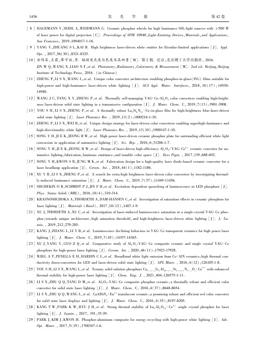
1456㊀发㊀㊀光㊀㊀学㊀㊀报第42卷[8]HAGEMANN V,SEIDL A,WEIDMANN G.Ceramic phosphor wheels for high luminance SSL-light sources with>500Wof laser power for digital projection[C].Proceedings of SPIE10940,Light-Emitting Devices,Materials,and Applications, San Francisco,2019:1094017-1-16.[9]YANG Y,ZHUANG S L,KAI B.High brightness laser-driven white emitter for Etendue-limited applications[J].Appl.Opt.,2017,56(30):8321-8325.[10]金伟其,王霞,廖宁放,等.辐射度光度与色度及其测量[M].第2版.北京:北京理工大学出版社,2016.JIN W Q,WANG X,LIAO N F,et al.Photometry,Radiometry,Colorimetry&Measurement[M].2nd ed.Beijing:Beijing Institute of Technology Press,2016.(in Chinese)[11]ZHENG P,LI S X,WANG L,et al.Unique color converter architecture enabling phosphor-in-glass(PiG)films suitable forhigh-power and high-luminance laser-driven white lighting[J].ACS Appl.Mater.Interfaces,2018,10(17):14930-14940.㊀[12]WANG J C,TANG X Y,ZHENG P,et al.Thermally self-managing YAGʒCe-Al2O3color converters enabling high-bright-ness laser-driven solid state lighting in a transmissive configuration[J].J.Mater.Chem.C,2019,7(13):3901-3908.[13]YOU S H,LI S X,ZHENG P,et al.A thermally robust La3Si6N11ʒCe-in-glass film for high-brightness blue-laser-drivensolid state lighting[J].Laser Photonics Rev.,2019,13(2):1800216-1-10.[14]ZHENG P,LI S X,WEI R,et al.Unique design strategy for laser-driven color converters enabling superhigh-luminance andhigh-directionality white light[J].Laser Photonics Rev.,2019,13(10):1900147-1-10.[15]SONG Y H,JI E K,JEONG B W,et al.High power laser-driven ceramic phosphor plate for outstanding efficient white lightconversion in application of automotive lighting[J].Sci.Rep.,2016,6:31206-1-7.[16]SONG Y H,JI E K,JEONG B W,et al.Design of laser-driven high-efficiency Al2O3/YAGʒCe3+ceramic converter for au-tomotive lighting:fabrication,luminous emittance,and tunable color space[J].Dyes Pigm.,2017,139:688-692. [17]SONG Y H,KWON S B,JUNG M K,et al.Fabrication design for a high-quality laser diode-based ceramic converter for alaser headlamp application[J].Ceram.Int.,2018,44(1):1182-1186.[18]XU Y R,LI S X,ZHENG P,et al.A search for extra-high brightness laser-driven color converters by investigating thermal-ly-induced luminance saturation[J].J.Mater.Chem.C,2019,7(37):11449-11456.[19]SHCHEKIN O B,SCHMIDT P J,JIN F H,et al.Excitation dependent quenching of luminescence in LED phosphors[J].Phys.Status Solidi(RRL),2016,10(4):310-314.[20]KRASNOSHCHOKA A,THORSETH A,DAM-HANSEN C,et al.Investigation of saturation effects in ceramic phosphors forlaser lighting[J].Materials(Basel),2017,10(12):1407-1-9.[21]XU J,THORSETH A,XU C,et al.Investigation of laser-induced luminescence saturation in a single-crystal YAGʒCe phos-phor:towards unique architecture,high saturation threshold,and high-brightness laser-driven white lighting[J].J.Lu-min.,2019,212:279-285.[22]KANG J,ZHANG L,LI Y B,et al.Luminescence declining behaviors in YAGʒCe transparent ceramics for high power laserlighting[J].J.Mater.Chem.C,2019,7(45):14357-14365.[23]XU J,YANG Y,GUO Z Q,et parative study of Al2O3-YAGʒCe composite ceramic and single crystal YAGʒCephosphors for high-power laser lighting[J].Ceram.Int.,2020,46(11):17923-17928.[24]WIEG A T,PENILLA E H,HARDIN C L,et al.Broadband white light emission from CeʒAlN ceramics:high thermal con-ductivity down-converters for LED and laser-driven solid state lighting[J].APL Mater.,2016,4(12):126105-1-8.[25]YOU S H,LI S X,WANG L,et al.Ternary solid solution phosphors Ca1-x-y Li x Al10-x-y Si1+x+y N3-y O yʒCe3+with enhancedthermal stability for high-power laser lighting[J].Chem.Eng.J.,2021,404:126575-1-11.[26]LI S X,ZHU Q Q,TANG D M,et al.Al2O3-YAGʒCe composite phosphor ceramic:a thermally robust and efficient colorconverter for solid state laser lighting[J].J.Mater.Chem.C,2016,4(37):8648-8654.[27]LI S X,ZHU Q Q,WANG L,et al.CaAlSiN3ʒEu2+translucent ceramic:a promising robust and efficient red color converterfor solid state laser displays and lighting[J].J.Mater.Chem.C,2016,4(35):8197-8205.[28]KANG T W,PARK K W,RYU J H,et al.Strong thermal stability of Lu3Al5O12ʒCe3+single crystal phosphor for laserlighting[J].J.Lumin.,2017,191:35-39.[29]PARK J,KIM J,KWON H.Phosphor-aluminum composite for energy recycling with high-power white lighting[J].Adv.Opt.Mater.,2017,5(19):1700347-1-6.㊀第10期郑㊀鹏,等:Ce 3+和Eu 2+掺杂荧光材料的光猝灭机理研究进展1457㊀[30]LENEF A,KELSO J,ZHENG Y,et al .Radiance limits of ceramic phosphors under high excitation fluxes [C].Proceedings of SPIE 8841,Current Developments in Lens Design and Optical Engineering ⅩⅣ,San Diego ,2013:884107-1-20.[31]LENEF A,RAUKAS M,WANG J,et al .Phosphor performance under high intensity excitation by InGaN laser diodes [J].ECS J.Solid State Sci.Technol .,2020,9(1):016019-1-16.[32]JANSEN T,BÖHNISCH D,JÜSTEL T.On the photoluminescence linearity of Eu 2+based LED phosphors upon high excita-tion density [J].ECS J.Solid State Sci.Technol .,2016,5(6):R91-R97.[33]VAN DER HEGGEN D,JOOS J J,SMET P F.Importance of evaluating the intensity dependency of the quantum efficien-cy:impact on LEDs and persistent phosphors [J].ACS Photonics ,2018,5(11):4529-4537.[34]BICANIC K T,LI X Y,SABATINI R P,et al .Design of phosphor white light systems for high-power applications [J].ACS Photonics ,2016,3(12):2243-2248.[35]SIJBOM H F,JOOS J J,MARTIN L I D J,et al .Luminescent behavior of the K 2SiF 6ʒMn 4+red phosphor at high fluxes and at the microscopic level [J].ECS J.Solid State Sci.Technol .,2015,5(1):R3040-R3048.[36]NITTA M,NAGAO N,NOMURA Y,et al .High-brightness red-emitting phosphor La 3(Si,Al)6(O,N)11ʒCe 3+for next-generation solid-state light sources [J].ACS Appl.Mater.Interfaces ,2020,12(28):31652-31658.[37]ZHENG P,LI S X,TAKEDA T,et al .Unraveling the luminescence quenching of phosphors under high-power-density exci-tation [J].Acta Mater .,2021,209:116813.[38]BRIL A.On the saturation of fluorescence with cathode-ray excitation [J].Physica ,1949,15(3-4):361-379.[39]DE LEEUW D M,HOOFT G W T.Method for the analysis of saturation effects of cathodoluminescence in phosphors;ap-plied to Zn 2SiO 4ʒMn and Y 3Al 5O 12ʒTb [J].J.Lumin .,1983,28(3):275-300.[40]JACOBS R R,KRUPKE W F,WEBER M J.Measurement of excited-state-absorption loss for Ce 3+in Y 3Al 5O 12and impli-cations for tunable 5d ң4f rare-earth lasers [J].Appl.Phys.Lett .,1978,33(5):410-412.[41]MINISCALCO W J,PELLEGRINO J M,YEN W M.Measurements of excited-state absorption in Ce 3+ʒYAG [J].J.Appl.Phys .,1978,49(12):6109-6111.[42]OWEN J F,DORAIN P B,KOBAYASI T.Excited-state absorption in Eu +2ʒCaF 2and Ce +3ʒYAG single crystals at 298and 77K [J].J.Appl.Phys .,1981,52(3):1216-1223.[43]HAMILTON D S,GAYEN S K,POGATSHNIK G J,et al .Optical-absorption and photoionization measurements from the excited states of Ce 3+ʒY 3Al 5O 12[J].Phys.Rev .B,1989,39(13):8807-8815.[44]LAWSON J K,PAYNE S A.Excited-state absorption of Eu 2+-doped materials [J].Phys.Rev .B,1993,47(21):14003-14010.[45]AUZEL F.Upconversion and anti-Stokes processes with f and d ions in solids [J].Chem.Rev .,2004,104(1):139-174.[46]VAN DER HEGGEN D,JOOS J J,BURBANO D C R,et al .Counting the photons:determining the absolute storage capacity ofpersistent phosphors [J].Materials (Basel ),2017,10(8):867-1-13.[47]STRUCK C W,FONGER W H.Unified model of the temperature quenching of narrow-line and broad-band emissions [J].J.Lumin .,1975,10(1):1-30.[48]BLEIJENBERG K C,BLASSE G.QMSCC calculations on thermal quenching of model phosphor systems [J].J.Solid State Chem .,1979,28(3):303-307.[49]DORENBOS P.Thermal quenching of Eu 2+5d-4f luminescence in inorganic compounds [J].J.Phys .:Condens.Mat-ter .,2005,17(50):8103-8111.[50]UEDA J,DORENBOS P,BOS A J J,et al .Insight into the thermal quenching mechanism for Y 3Al 5O 12ʒCe 3+through ther-moluminescence excitation spectroscopy [J].J.Phys.Chem .C,2015,119(44):25003-25008.[51]BACHMANN V,RONDA C,MEIJERINK A.Temperature quenching of yellow Ce 3+luminescence in YAGʒCe [J].Chem.Mater .,2009,21(10):2077-2084.郑鹏(1991-),男,安徽亳州人,博士研究生,2014年于北京科技大学获得硕士学位,主要从事激光照明与显示用荧光材料的研究㊂E-mail:zheng_peng@foxmail.com解荣军(1969-),男,江苏镇江人,博士,教授,1998年于中国科学院上海硅酸盐研究所获得博士学位,主要从事稀土发光材料㊁量子点和发光器件的研究㊂E-mail:rjxie@第42卷㊀第10期2021年10月发㊀光㊀学㊀报CHINESE JOURNAL OF LUMINESCENCEVol.42No.10Oct.,2021文章编号:1000-7032(2021)10-1458-24㊀㊀收稿日期:2021-06-02;修订日期:2021-07-01㊀㊀基金项目:国家自然科学基金(61975070,51902143,61971207);江苏省高校优势学科建设项目(PAPD);江苏省重点研发项目(BE2018062,BE2019033);江苏省自然科学基金(BK20191467);江苏省国际科技合作项目(BZ2019063,BZ2020045,BZ2020030);徐州市技术创新专项(KC19250,KC20201,KC20244);江苏省研究生科研与实践创新计划项目(SJCX21_1137)资助Supported by National Natural Science Foundation of China(61975070,51902143,61971207);Priority Academic Program Devel-opment of Jiangsu Higher Education Institutions (PAPD );Key Research and Development Project of Jiangsu Province (BE2018062,BE2019033);Natural Science Foundation of Jiangsu Province(BK20191467);International S&T Cooperation Pro-gram of Jiangsu Province (BZ2019063,BZ2020045,BZ2020030);Special Project for Technology Innovation of Xuzhou City (KC19250,KC20201,KC20244);Postgraduate Research &Practice Innovation Program of Jiangsu Province(SJCX21_1137)高功率密度激发荧光材料的反常热猝灭效应张曦月1,张㊀乐1∗,孙炳恒2,马跃龙1,3,康㊀健1,侯㊀晨1,姜本学2∗,刘永福4∗,陈㊀浩1(1.江苏师范大学物理与电子工程学院,江苏省先进激光材料与器件重点实验室,江苏徐州㊀221116;2.中国科学院上海光学精密机械研究所,上海㊀201800;3.江苏大学机械工程学院,江苏镇江㊀212013;㊀4.中国科学院宁波材料技术与工程研究所,浙江宁波㊀315201)摘要:荧光转换材料普遍存在的发光强度随温度升高而降低的热猝灭现象严重影响了器件的性能,限制了其在高功率发光二极管(LED)/激光二极管(LD)照明中的应用㊂然而,部分荧光材料却会出现随着温度升高发光强度增大的现象,即反常热猝灭效应㊂反常热猝灭作为提升发光材料及其器件应用性能的有效途径得到了广泛研究㊂本文总结了目前反常热猝灭效应在发光领域的研究现状及应用,阐述了发光反常热猝灭的机理,并对其未来发展趋势进行了展望,以期开发出具有更优反常热猝灭特性的新型发光材料,满足高效高功率LED /LD 照明器件的应用需求㊂关㊀键㊀词:高功率密度;LED /LD 照明;热猝灭现象;反常热猝灭效应中图分类号:O482.31㊀㊀㊀文献标识码:A㊀㊀㊀DOI :10.37188/CJL.20210202Abnormal Thermal Quenching Effect ofHigh Power Density Excited Fluorescent MaterialsZHANG Xi-yue 1,ZHANG Le 1∗,SUN Bing-heng 2,MA Yue-long 1,3,KANG Jian 1,HOU Chen 1,JIANG Ben-xue 2∗,LIU Yong-fu 4∗,CHEN Hao 1(1.Jiangsu Key Laboratory of Advanced Laser Materials and Devices ,School of Physics Electronic Engineering ,Jiangsu Normal University ,Xuzhou 221116,China ;2.Shanghai Institute of Optics Fine Mechanics ,Chinese Academy of Sciences ,Shanghai 201800,China ;3.School of Mechanical Engineering ,Jiangsu University ,Zhenjiang 212013,China ;4.Ningbo Institute of Materials Technology &Engineering ,Chinese Academy of Sciences ,Ningbo 315201,China )∗Corresponding Authors ,E-mail :zhangle @ ;jiangsic @ ;liuyongfu @Abstract :Thermal quenching is a phenomenon that the luminescence intensity of fluorescent con-version materials decreases with the increase of temperature,and it seriously affects the performance of the devices and limits the applications in high power LED /LD lighting.However,the lumines-cence intensity of some fluorescent materials often increases with the rise of temperature,which is named as the abnormal thermal quenching effect.As an effective way to improve the performance ofluminescent materials and devices,the abnormal thermal quenching effect has been widely studied.㊀第10期张曦月,等:高功率密度激发荧光材料的反常热猝灭效应1459㊀In this paper,the research status and application of fluorescent materials with abnormal thermal quenching effect was reviewed,the mechanism of abnormal thermal quenching effect was illustrated, and its future development trend was prospected.This review will help to develop new luminescent materials with better abnormal thermal quenching characteristics to meet the application requirements of high efficiency and high power LED/LD lighting devices.Key words:high power density;LED/LD lighting;thermal quenching phenomenon;abnormal thermal quenching effect1㊀引㊀㊀言白光发光二极管(Light emitting diodes,LED)作为第四代照明光源,在固态照明与显示领域已经得到了长时间的发展与应用[1-13]㊂相比LED,基于激光二极管(Laser diode,LD)芯片的照明技术因其体积小㊁亮度高㊁照射距离远等优点在高功率照明㊁显示和光通讯等众多领域具有广泛的应用前景[14-17]㊂目前,蓝光芯片搭配黄色荧光材料是白光LED/LD的主流实现方案[18],荧光材料作为LD器件的主要组成部分,其性能直接决定了照明器件的品质㊂然而,在激光照明等应用场景中,高功率密度激发会引起荧光材料温度上升,导致发光离子的激发态电子非辐射分布增加[1,19],在150~200ħ的范围内发射强度降低至其初始状态60%~70%以下,即产生显著的热猝灭(Ther-mal quenching,TQ)现象㊂高功率密度激发下温度上升带来的热猝灭行为严重影响着LED/LD用荧光材料的服役稳定性,包括发光强度降低㊁色度漂移㊁发光饱和等一系列问题,从而导致目前已有荧光材料的商业应用受到限制[20]㊂因此,解决荧光材料的热猝灭问题,寻找和开发在高功率密度激发下拥有更优耐热特性的荧光材料以缓解高功率密度激发下热效应带来的不利影响,将成为新的研究热点㊂反常热猝灭效应,即在一定温度范围内,随着工作温度上升,荧光材料的发射强度保持不变或逐渐增加的发光现象㊂在高功率密度激发下,荧光材料的反常热猝灭效应有利于提高材料的发光量子效率和热稳定性,避免由于光转换过程中积累的热量带来的荧光材料运行温度不断升高,最终引起激光照明器件的发光强度达到峰值,并开始骤降的问题;亦可以缓解由于功率增加造成的色光比例改变,导致色温㊁色坐标㊁显色指数发生显著变化的问题,提升高功率密度激发下荧光材料的发光品质㊂自从2017年Kim等[13]发现了一种在200ħ温度下仍能保持室温发射强度100%的蓝光Na3Sc2(PO4)3ʒ0.03Eu2+荧光粉,反常热猝灭荧光材料便受到了广泛关注㊂在高功率密度激发下出现反常热猝灭效应㊁保持优越的发光性能的荧光材料无疑具有非常光明的发展前景㊂本文从材料组分掺杂改性㊁复合结构设计方面概述了近年来反常热猝灭效应机理的研究进展,对几种典型的反常热猝灭体系的结构㊁发光性质及其实际应用进行了详细介绍,并讨论了目前本领域研究中存在的问题及发展趋势,以期可以采用新的方法与角度更好地理解高功率密度激发下荧光材料的反常热猝灭效应,设计开发出新型的无热猝灭或负热猝灭的高效荧光材料,满足其在高功率密度激发照明与显示等领域的应用㊂2㊀反常热猝灭效应机理相关研究一般来说,热猝灭现象与高温工作状态下激活离子激发态和基态能级间的交叉弛豫㊁热离化等过程密切相关[19,21-22]㊂研究表明,较大的电离能(激活剂离子的发射能级和导带底之间的能量差)㊁较大的热猝灭活化能㊁较宽的禁带宽度等条件下更容易抑制热猝灭现象,减少无辐射跃迁过程[23-24]㊂科研人员对于缓解热猝灭效应做出的诸多努力催生了荧光材料中反常热猝灭效应的发现,有效改善了高功率密度激发下荧光材料的发光性能㊂全面分析荧光材料的电子结构和光学性质有助于认识热猝灭现象的形成机制,更深入理解反常热猝灭效应的作用机理,并指导开发热猝灭性能更加良好的新型荧光材料㊂结合存在反常热猝灭效应荧光材料的相关文献报道,增强反常热猝灭效应的工作主要围绕材料组分设计(掺杂改性)和复合结构设计两个途径开展㊂因此,本文对反常热猝灭机理的解释将按照以上两个方面进行归纳总结㊂1460㊀发㊀㊀光㊀㊀学㊀㊀报第42卷2.1㊀荧光材料组分设计目前LED /LD 用稀土荧光材料主要是使用稀土发光离子中属于非禁戒的f-d 电子跃迁的激活剂,包括Eu 2+㊁Ce 3+和Yb 2+㊂由于其5d 轨道裸露在4f 电子层外,极易受到外部环境的影响,因此通过调节基质的晶体结构可以实现荧光材料性能的调节和优化[25]㊂对稀土荧光材料进行离子掺杂或原子取代调整其化学结构组分,调控影响其热稳定性的关键参数,利用不同的作用机制实现反常热猝灭效应㊂目前通过荧光材料组分设计实现反常热猝灭效应的机制可以分为下述5种㊂2.1.1㊀缺陷能级到发光中心激发能级的能量转移对于下转移或下转换发光,其过程是在短波激发下,发光离子的基态电子跃迁至激发态,随后跃迁至基态并产生长波发射㊂然而,在高功率密度激发特别是激光照明应用中,过高的工作温度与过强的激发光泵浦密度使得处于激发态能级的电子二次跃迁至导带上,随后以无辐射跃迁的形式回到基态,造成热猝灭现象㊂图1为荧光材料中典型的缺陷能级向发光中心激发能级能量传递示意图㊂在低温范围内,通过在荧光材料中引入缺陷作为陷阱能级,部分电子被诱导捕获并存储在陷阱能级里㊂热刺激后,被捕获电子从陷阱能级跃出,随后通过导带转移到发光离子的激发态能级从而实现发光过程㊂因此,电子被陷阱能级俘获与电子从陷阱解俘的过程达到动态平衡,此时便出现零猝灭甚至负猝灭现象[26]㊂从陷阱到发光中心发生了有效的能量转移,形式上为发光离子提供了额外的激发能,从图1㊀缺陷能级向发光中心激发能级的能量传递示意图Fig.1㊀Schematic diagram of energy transfer from defect levelto excitation level of emission center而产生更强的发光㊂因此,陷阱能级的深度和浓度成为影响反常热猝灭效应的关键㊂在荧光材料中,充当电子陷阱的缺陷能级可以通过以下方式引入:(1)离子非等价取代引入缺陷作为电子陷阱晶格内部离子半径相近的情况下易发生非等价取代,即高价离子取代低价离子形成正缺陷,或低价离子取代高价离子形成负缺陷㊂而非等价的格点取代导致的电荷不平衡会诱导带电属性相反的缺陷产生,增加电子陷阱深度和数量,在热激活下充当陷阱的晶格缺陷释放载流子,抑制热猝灭现象的出现㊂北京科技大学夏志国教授团队[23]采用Eu 2+离子取代K +离子产生正缺陷Eu ㊃K ,加之制备过程中存在的V ㊃㊃O ,都会诱导负缺陷Vᶄk 的产生,合成的K 2BaCa(PO 4)2ʒ3%Eu 2+蓝光荧光粉在275ħ时TQ 为零㊂如图2所示,结合PBE0杂化泛函的密度泛函(DFT)计算得到的缺陷转变能级与热释光谱的测量结果,推测在零热猝灭的初始上升阶段所涉及的缺陷最有可能是基体材料中的氧空位㊂氧空位作为导带的电子陷阱中心捕获电子,通过能量传递补偿热猝灭效应㊂之后,该团队[27]将Li +掺杂进NaAlSiO 4ʒEu实现了量子效率(QE)的提高㊁光致发光(PL)特性的可调谐和热稳定性的提升,当N ѲASOʒy Li,Eu 中(Ѳ表示V NA )y =0.15时,在150ħ时仍能保持室温条件下94.6%㊂DFT 计算结果表明,Li 倾向的占位为Li Al -2Li VNa ,Li 含量越多,发光热稳定性越高㊂这是由于Li 的相关陷阱(如位于V Na 格点的Li)受热释放出更多电子与Eu 2+重组,传递至Eu 2+的5d 激发态能级㊂兰州大学王育华教授团队[28]采用Eu 2+离子取代K +离子,Sc 3+离子取代Hf 4+离子形成缺陷Eu ㊃K 和ScᶄHf ,进而分别诱导产生负空位缺陷Vᶄk 和正空位缺陷V ㊃㊃O 以保持电中性㊂合成的近紫外和蓝光激发绿光荧光粉K 2HfSi 3O 9ʒ2%Eu 2+,6%Sc 3+在200ħ时仍不存在发光损耗㊂结合25~250ħ的热释光谱和衰减曲线分析,陷阱能级的存在使其与Eu 2+的5d 能级之间发生能量转移㊂之后,该团队[29]采用Ce 3+离子不等价取代Li 2CaSi 2N 4的Ca 2+格点,产生Ce ㊃Ca 和VᵡCa 缺陷㊂合成的Li 2CaSi 2N 4ʒCe 3+荧光粉在200ħ时零热猝㊀第10期张曦月,等:高功率密度激发荧光材料的反常热猝灭效应1461㊀图2㊀(a)KBCPʒ3%Eu 2+的热释光曲线;(b)DFT 计算KBCP 中V K2,3和V O1,2的热力学转变能级示意图[23]㊂Fig.2㊀(a)TL curve and its deconvolutions of KBCPʒ3%Eu 2+.(b)Schematic representation of calculated thermodynamiccharge transition levels for V K2,3and V O1,2in KBCP using the DFT-PBE0method [23].灭㊂在150ħ时,Li 2CaSi 2N 4ʒ0.05Ce 3+在507nm 和557nm 处的发射峰仍然保持初始强度的95%和104%,表现出良好的热稳定性㊂昆明理工大学邱建备教授团队[30]通过在Sr 3SiO 5ʒEu 2+中引入Tm 3+占据Sr 2+格点,Tm 3+的引入产生了一种具有更深陷阱深度的缺陷结构,可以有效地捕获载流子,从而抑制了非辐射过程中声子形式的能量损失㊂热扰动产生的载流子补偿了热猝灭行为,在120ħ内仍零猝灭㊂西北农林科技大学周文明教授团队[31]采用Eu 3+离子取代Ca 2+离子的格点,不平衡的电荷取代导致了空位缺陷(VᵡCa )缺陷和间隙缺陷(Oᵡi )的产生,晶格缺陷作为电子陷阱受热释放载流子,补偿了热猝灭效应㊂合成的红色荧光粉Ca 2InSbO 6ʒEu 3+在207ħ时的发射强度是27ħ时的1.1倍㊂因此,采取非等价取代引入缺陷作为电子陷阱是一种有效的方法㊂然而,过高的非等价取代浓度会对晶格结构产生不利影响㊂同时,缺陷浓度增大也将不可避免地会造成发光湮灭,反而达不到捕获电荷的效果㊂(2)阳离子无序化增加陷阱的深度和数量通过引入阳离子取代晶格中部分初始阳离子的格位,实现一定程度的阳离子无序化,实际上改变了平均离子半径,以调整晶格应变㊂引入阳离子无序化不仅会导致材料结构刚性的变化,通过破坏晶格振动来抑制无辐射过程,而且导致作为电子陷阱的缺陷数量和深度增加㊂在有序化合物中,有序度可以用来表征不同原子在晶格格点中的优先占位情况㊂在固溶体A 1-xB x 中,有序度η根据以下公式计算[32-33]:η=O CC A A -O CC B A =O CC B B -O CC AB ,(1)O CC A A ㊁O CC B A ㊁O CC B B 和O CC AB 表示A 原子和B 原子分别占据A 格点或B 格点㊂刘泉林教授团队[33]计算了在(Ba 1-x Sr x )2SiO 4ʒEu 2+中Sr 2+取代Ba 2+的阳离子有序度,当x 为0.5时,其在150ħ时的发射光强度仍保持在90%以上㊂中国台湾大学刘如熹教授团队[34]通过Ca 0.55Ba 0.45组合取代Sr 1.98Si 5N 8ʒEu 0.02中的Sr 2+,在一定程度上引入阳离子创造无序环境,在25~200ħ工作温度范围内,发光强度增加了20%~26%㊂在此基础上,Kim 等[35]通过在固溶体荧光粉Lu 2.8Ca 0.1Ce 0.1Al 1.8Ba 0.2Al 2.7Si 0.3O 12中掺杂Ba 2+部分取代Al 3+引入阳离子无序效应,将其发光强度提升至商用LuAG ʒCe 3+(Lu 3Al 5O 12ʒCe 3+)的116%㊂引入阳离子无序化可以增加陷阱的深度和数量,有效抑制无辐射过程㊂相比异价离子取代,同价离子取代的浓度可相对较高㊂然而,当引入的阳离子与晶格中初始阳离子半径差值超过一定值时会在晶格中产生杂相,且原子占位的优先级往往不易调控㊂此外,引入阳离子无序化在产生电子陷阱的同时有可能对晶格结构刚性产生负面影响㊂因此,该方法研究相对较少㊂(3)特定温度下的结构相变形成空位等缺陷当阳离子无序化增大到一定阶段时,晶格将产生结构相变㊂随着温度的升高,荧光材料从有序到无序的相变带来的结构差异导致电导率㊁发射强度和缺陷数量都发生变化,从而影响荧光材1462㊀发㊀㊀光㊀㊀学㊀㊀报第42卷料的性能㊂2017年,Kim等[13]将Eu2+离子掺入蓝光荧光粉合成了Na3Sc2(PO4)3ʒ0.03Eu2+,温度升高使得Na+无序化导致了α相ңβ相ңγ相的相变,增加了阳离子空位缺陷,从而形成了作为电子捕获中心的缺陷能级的产生,在200ħ时实现了零猝灭㊂这一过程可通过方程式2Na++Eu2+ңEu㊃Na+VᶄNa进行简单描述㊂这有利于能量从包含电子空穴对的陷阱到Eu2+5d能级的转移,从而补偿非辐射跃迁引起的发射损失,在温度上升时维持发射强度,展示出了零猝灭的性质㊂电子陷阱的深度可以通过如下公式估计:E=T M/500,(2)其中E代表激活能,即陷阱深度,单位为eV;T M代表热释光曲线中峰值对应的温度,单位为K[36]㊂随后,天津理工大学王达健教授团队[37]也对Na3Sc2(PO4)3ʒEu2+荧光材料中出现反常热猝灭效应进行了研究,也得到了升温过程导致相变㊁抑制无辐射跃迁过程的结论㊂荧光材料在特定温度下的结构相变有助于形成空位等缺陷,结构差异会导致作为电子陷阱的缺陷数量增加,有效补偿热猝灭效应㊂然而,研究特定温度下荧光材料的相变对其发光性能的影响相对较少,且研究的材料体系相对单一㊂目前,由于涉及缺陷态的热猝灭现象往往难以通过实验手段进行微观层面上的深度研究,而理论计算可以作为一种深入了解和分析缺陷的辅助手段㊂苏州大学孙洪涛教授团队[38]采用DFT 计算分析了(C9NH20)2SnBr4晶体的能级情况,发现引入Br1和/或Br2空位会在带隙中产生缺陷能级,而单独引入C9NH20空位则不会,这直接导致了在270nm激发下,在-268~25ħ的温度区间内仅加入溴源的(C9NH20)2SnBr4单晶出现负猝灭现象,在25~50ħ的温度区间内热猝灭现象也有明显改善㊂该材料仅在11ħ的室温下即可制备,且展现出优异的抗热猝灭性能,具有较好的应用前景㊂近期,瑞典Linderälv等[39]借助第一性原理计算得到了Ce与氧空位间电荷转移的最低能量路径,从理论层面研究了CeʒYAG中氧空位作为深度缺陷态参与发光热猝灭的复合机制㊂基于密度泛函理论的第一性原理计算可以弥补实验的不足,但是由于稀土离子4f电子具有开壳层特征,当其共掺杂入荧光材料中,会大大增加理论模拟的计算量,因此往往需要经验模型辅助,这导致理论计算存在一定的局限性㊂2.1.2㊀提升晶格结构刚性来抑制无辐射跃迁过程荧光材料的结构刚性是判断材料晶格骨架结构是否稳定的有效指标,尤其是在高功率密度激发下,高结构刚性和晶格对称性的荧光材料有利于降低晶格振动频率,抑制无辐射衰减过程,减少声子损耗㊂影响发光材料的晶格刚性主要包括晶格联通程度㊁化学键健能等㊂此外,依据 尺寸匹配原则 以及 泡利经验式I=1-exp(-Δx2/4) (Δx为泡利电负性差)[40],选取与所替换离子半径差在15%以内并且与氧原子间具有更强键能以及共价性的离子,可有效提升晶格排列紧实程度,抑制极端服役条件下由热量引发的晶格振动,缓解无辐射跃迁效应,提升发光材料的热稳定性能,这使得其在高功率密度激发下往往易出现反常热猝灭效应㊂通过实验和DFT计算得到的德拜温度(ΘD)可以作为衡量晶体结构刚性的关键参数[41-43],荧光材料的高德拜温度对应于低晶格振动频率和小斯托克斯位移[12],这往往会降低无辐射跃迁的可能性,因此德拜温度可以帮助衡量和筛选猝灭性能相对较好的基质材料㊂通过准谐德拜模型可以得到德拜温度(ΘD),可由公式(3)和(4)计算得到[44-45]:ΘD=h kB(6π2V1/2n)1/3f(σ)B s M,(3) f(σ)={32231+σ1-2σ()3/2+131+σ1-σ()3/2[]-1}1/3,(4)其中k B和h分别表示简化后的波尔兹曼常数和普朗克常数,M为原胞的相对分子质量,B s为晶体的绝热体弹模量,n是每个原胞中包含的原子数, V表示原胞的体积,σ是泊松比㊂Brgoch等[46]指出,荧光材料中多面体连通度高的晶格可以有效限制振动自由度,降低声子参与的无辐射弛豫过程,这使得这类荧光材料通常具有良好的猝灭特性㊂基于此,荧光材料中石榴石型㊁UCr4C4型和β-K2SO4型都是结构刚性较优异的结构㊂(1)石榴石型石榴石型矿物结构原型属于立方晶系,空间㊀第10期张曦月,等:高功率密度激发荧光材料的反常热猝灭效应1463㊀群为Ia 3d ㊂其一般公式是A 3B 2C 3O 12,其中A ㊁B 和C 是位于不同对称位置的阳离子㊂A 原子占据了8配位十二面体的24(c)格点,B 原子占据了6配位八面体的16(a)格点,C 原子占据了四配位四面体的24(d)格点㊂每个八面体与6个四面体相连,而每个四面体通过公共角与4个[AlO 6]八面体相连[47-50]㊂正是由于三种不同阳离子格位的存在,使得掺Ce 3+的石榴石可以通过不同阳离子的替代灵活地调整和优化特定应用场景下所需的发光性能㊂作为石榴石的主要体系,YAG 的德拜温度高达726K,这大大降低了无辐射跃迁的概率,也使其保持了较高的量子产率,从而使其在激光领域作为增益介质的基质材料具有广泛应用[51-52]㊂该结构的典型应用将在3.1部分介绍㊂(2)β-K 2SO 4型β-K 2SO 4矿物结构原型属于正交晶系,空间群为Pnam [53]㊂典型的两类包括正硅酸盐A 2SiO 4型(A =Sr,Ba)ʒEu(Eu 取代Sr 或Ba 位)和磷酸盐AB PO 4型(A 是一价阳离子如Na +,K +;B 是二价阳离子如Ca 2+,Sr 2+,Ba 2+)[43,54-55]㊂在AB PO 4型磷酸盐体系中,随着A ㊁B 离子半径的变化而有所不同,其结构也会有所不同(橄榄石结构㊁钾芒硝结构等)㊂针对该体系,苏州大学黄彦林教授团队[54]的研究表明NaSrPO 4的热猝灭温度相较KBaPO 4低了200ħ,作者认为KBaPO 4和NaSrPO 4不同的热稳定性是由于在NaSrPO 4中Eu 2+占据多个Sr 2+格位导致分布在整个晶格上的 高度无序环境 中,而KBaPO 4ʒEu 2+离子单一格位在晶格中具有较高的 有序态 ㊂β-K 2SO 4矿物结构的典型应用将在3.2部分介绍㊂(3)UCr 4C 4型UCr 4C 4矿物结构原型属于四方晶系,空间群为I 4/m ,Cr 和C 相连形成CrC 4四面体,四面体相连构成骨架,U 离子填充在四面体之间㊂其化合物通式可写为Me (A ,B )4X 4,其中Me 为碱金属或碱土金属离子,A 和B 为配位离子㊂[AX 4]和[BX 4]四面体通过共边或共顶点连接形成[001]方向的vierer 环,Me 离子位于其形成的环状结构中,其格位具有高度对称性且致密度k =(AB/X )=1,因此拥有较强的结构刚性[25,56]㊂例如Sr-LiAl 3N 4ʒEu 2+(95%@227ħ)和RbLi(Li 3SiO 4)2ʒEu 2+(103%@150ħ),它们都属于UCr 4C 4型结构[11,57]㊂该结构的典型应用将在3.3部分介绍㊂除上述体系的荧光材料外,科研人员在其他体系中也进行了诸多研究㊂图3㊀(a)石榴石矿物结构模型[58];(b)UCr 4C 4矿物结构模型[59];(c)K 2SO 4矿物结构模型[23]㊂Fig.3㊀(a)Garnet mineral structure model [58].(b)UCr 4C 4mineral structure model [59].(c)K 2SO 4mineral structure model [23].。
热释光

热释光的测量系统组成
热释光测定装置构成 加热系统--电热盘 光测量 记录及数据处理系统光电倍增管 热信号为记录仪的x轴,热释光对温度 的反应强度为Y轴
光测量由探测、转换和记录三部分组成
光打到阴极,光子转换成电子(光电材料的 作用)
电子到达阳极,在阳极产生电子脉冲
阳极输出的信号通过脉冲放大器和甄别器把 选择出来的脉冲输入光子率表
在暗室红光中破碎并分选石英单矿物 样品磨至150 目左右 30%氟硅酸(20 mபைடு நூலகம்/g)溶蚀6 d 溶蚀长石颗粒 每个样品制10 片,每片的样品量为4mg 左
右 在暗室中用90Srβ源对样品进行不同剂量
的辐照 辐照完后在暗室中放置4 个星期, 然后进行
释光测定
测定过程
加热速度2K/ s 测定的光波波长范围300 —1000nm , 每
热释光的应用
热释光测年法范围 5000年到50000年 甚至50万年
采集样品
采样前用热释光剂量仪放在取样品的位 置上(几个月到一年)
测出一年的平均辐射剂量
获用闪烁计数器测定取样点的平均辐射 剂量(几分钟即可)
采样用不透光钢筒挤压取样,并密封 保证样品不受高温、各种光线的辐射
样品处理
(TL) – A radiometric dating technique
in which the amount of light energy released
when heating a sample
the amount of light energy is measured as an indicator of the time since it was last heated to a critical temperature
液压支架用防冻液的研制

第4期 收稿日期:2020-11-25作者简介:蔡淑红(1987—),女,河北迁安人,硕士,工程师,从事精细化学品的研发与检测工作。
液压支架用防冻液的研制蔡淑红,王 峰,石 晶,商 轶,侯锦锋,谭凯锋,刘波涛(中国船舶重工集团公司第七一八研究所,河北邯郸 056027)摘要:液压支架用防冻液作为液压支架系统内的传动介质,利用液体的压力或动能来传递能量。
本文通过对抗冻剂、抗磨剂和防腐防锈剂的筛选制备了一种液压支架用防冻液,有机酸盐、二元酸、三唑类添加剂和抗磨剂含量分别为0.2%,0.2%,0.02%和1%时,润滑性PB值可达556N,其它性能指标达到了MT76-2011的指标要求。
关键词:液压支架用防冻液;抗冻剂;抗磨剂;防腐防锈剂中图分类号:TE626.38 文献标识码:A 文章编号:1008-021X(2021)04-0015-02TheDevelopmentoftheAntifreezeUsedinHydraulicSupportCaiShuhong,WangFeng,Shijing,ShangYi,HouJinfeng,TanKaifeng,LiuBotao(The718thResearchInstituteofCSIC,Handan 056027China)Abstract:Asthetransmissionmediuminthehydraulicsupportsystem,theantifreezeusedinthehydraulicsupportusesthepressureorkineticenergyoftheliquidtotransmitenergy.Inthispaper,akindofantifreezeusedinthehydraulicsupportwaspreparedbyscreeningtheantifreeze,antiwearagent,anticorrosiveandantirustagent.Whenthecontentoforganicacidsalt,dibasicacid,threeazoleadditivesandantiwearagentwas0.2%,0.2%,0.02%and1%respectively,thePBvaluecouldreach556N,andotherperformancesofthefluidcouldmeetthestandardofMT76-2011.Keywords:theantifreezeusedinhydraulicsupport;antifreeze;antiwearagent;anticorrosiveandantirustagent 液压支架是靠液体压力进行工作的支护设备,在煤矿开采过程中可以保障工人的安全和各项工作的正常运行。
一种Y_型延迟荧光分子及其蓝光和绿光OLED_应用

第 45 卷第 1 期2024年 1 月Vol.45 No.1Jan., 2024发光学报CHINESE JOURNAL OF LUMINESCENCE一种Y型延迟荧光分子及其蓝光和绿光OLED应用孙静1,2*,樊志杰1,杜纪宽1,董海亮1,2,王华1,2*(1. 太原理工大学新材料界面科学与工程教育部重点实验室,山西太原 030024;2. 山西浙大新材料与化工研究院,山西太原 030024)摘要:以噻吨酮作为受体、3,6⁃(二咔唑基)三咔唑作为给体设计合成了一种具有延迟荧光特性的Y型分子(TX⁃TCz)。
模拟计算表明化合物HOMO和LUMO能级完全分离且在苯环上存在较小的重叠,有助于获得小的S1和T1的能级差ΔE ST。
随着溶剂极性的增加,化合物发射峰发生明显的红移且由于电荷转移态和局域激发态的共存产生了双峰发射。
在纯膜中TX⁃TCz的发射峰位于513 nm,量子产率为11.5%。
基于低温下荧光和磷光发射峰,计算得到化合物的ΔE ST为0.03 eV,并且检测到µs级的寿命,说明化合物具有延迟荧光发射。
与此同时,化合物展示了良好的热稳定性能和电化学性能,有助于制备高性能OLED器件。
其在掺杂浓度为5%(wt)的器件中展示了良好的蓝光性能,发射峰位于463 nm,最大外量子效率为1.53%;在非掺杂器件中展示了良好的绿光发射(522 nm),最大外量子效率达到1.81%。
关键词:OLED; Y型分子;蓝光/绿光;延迟荧光中图分类号:O625.6; TN383 文献标识码:A DOI: 10.37188/CJL.20230261A Y-type Delayed Fluorescence Emitter for Blue and Green OLEDsSUN Jing1,2*, FAN Zhijie1, DU Jikuan1, DONG Hailiang1,2, WANG Hua1,2*(1. Key Laboratory of Interface Science and Engineering in Advanced Materials, Ministry of Education,Taiyuan University of Technology, Taiyuan 030024, China;2. Shanxi-Zheda Institute of Advanced Materials and Chemical Engineering, Taiyuan 030024, China)* Corresponding Authors, E-mail: sunjing@; wanghua001@ Abstract:A novel Y-type emitter (TX-TCz) with delayed fluorescence characteristic was designed and synthesized using thioxanthone group as the acceptor and 6-(9H-carbazol-9-yl)-9H-3,9'-bicarbazole moiety as the donor. Theo⁃retical calculations showed the prominent separation of HOMO and LUMO levels with only a small overlap on the ben⁃zene ring, which helped to achieve the small energy band gap ΔE ST between the S1 and T1. With the increasing polari⁃ties of solvents, the emission peaks of TX-TCz exhibited an obvious red shift and dual emission peaks generated be⁃cause of the coexistence of charge transfer state and locally excited state. In the pure film, the emission peak of TX-TCz was located at 513 nm with the photoluminescence quantum yields (PLQY) of 11.5%. According to the fluores⁃cence and phosphorescence emission at low temperature, ΔE ST of 0.03 eV between S1 and T1 was calculated, at the same time µs magnitude lifetime was also detected. It indicated that TX-TCz had the considerable delayed fluores⁃cence characteristic. In addition, TX-TCz had good thermal stability and electrochemical properties, which was help⁃ful for the preparation of high-performance OLED devices. In the doped devices with the doping concentration of 5%(wt), TX-TCz showed excellent blue light performance with the emission peak at 463 nm and the maximum external quantum efficiency (EQE) of 1.53%. In the non-doped device, good green emission at 522 nm was obtained with a maximum EQE of 1.81%Key words:OLED; Y-type structure; blue/green light; delayed fluorescence文章编号: 1000-7032(2024)01-0078-08收稿日期:2023⁃10⁃27;修订日期:2023⁃11⁃15基金项目:国家自然科学基金(62074109,6207031407)Supported by National Natural Science Foundation of China(62074109,6207031407)第 1 期孙静,等:一种Y型延迟荧光分子及其蓝光和绿光OLED应用1 引 言有机电致发光器件(Organic light emitting di⁃odes,OLEDs)具有轻薄美观、对比度高、环境友好等优点,在柔性照明和显示领域展示了广阔的应用前景[1-4]。
抗肿瘤肽露那辛研究进展

抗肿瘤肽露那辛研究进展
陈琛
【期刊名称】《中国生化药物杂志》
【年(卷),期】2010(31)4
【摘要】露那辛(Lunasin)是一个从大豆、大麦、小麦、苋菜、中草药种子和其它植物源种子分离纯化得到的含43个氨基酸,相对分子质量为4800的非常有前景的抗肿瘤多肽.Lunasin多肽羧基端有9个天冬氨酸(Asp);结构中包含细胞黏附基序"Arg-Gly-Asp";Lunasin中的螺旋结构可能是染色体结合蛋白的保守区.目前已经研究证实Lunasin肽具有抗炎和抗癌活性.此文综述了Lunasin的发现、特性、生物药效、来源及在植物中的舍量,以期为Lunasin的研究提供参考.
【总页数】4页(P281-284)
【作者】陈琛
【作者单位】陕西理工学院,陕西省资源生物重点实验室,陕西,汉中,723000
【正文语种】中文
【中图分类】R979.1;R285
【相关文献】
1.露那辛功能肽的研究进展 [J], 张中义;邵文科;闫溢哲;柴颖
2.大豆活性肽露那辛的研究进展 [J], 孙晓燕;张志国
3.文化冲突与身份认同危机——《露辛达·布雷福特》中露辛达和斯蒂芬母子悲剧命运根源的解读 [J], 周明珠
4.从女性主义和后殖民主义的话语融合角度看《露辛达·布雷福特》--“他者”话语
在露辛达身上的交汇 [J], 赵姗
5.文化冲突与身份认同危机——《露辛达·布雷福特》中露辛达和斯蒂芬母子悲剧命运根源的解读 [J], 周明珠
因版权原因,仅展示原文概要,查看原文内容请购买。
石墨烯修饰的电化学免疫传感器在肿瘤标志物检测中的应用_曾莉

肿 瘤 标 志 物 是 指 在 肿 瘤 的 发 生 和 增 殖 过 程 中 ,由 肿 瘤 细 胞 本 身 所 产 生 的 或 者 是 由 机 体 对 肿 瘤 细 胞 反 应 而 产 生 的 ,反 映 肿 瘤 存 在 和 生 长 的 一 类 物 质 。 其 在 肿 瘤 普 查 、诊 断 、判 断 预 后 、评 价疗效和高危人群随访观察等方面都具有较大的实用价值。 目前检测方法主要有放 射 免 疫 分 析 法、免 疫 放 射 分 析 法、酶 标 记免疫分析法、化学免 疫 发 光 分 析 法、时 间 分 辨 荧 光 免 疫 分 析 法、蛋白芯片检测法,这 些 方 法 存 在 灵 敏 度 低、特 异 度 低、放 射 性损害、反应条件严 格、操 作 繁 琐、分 析 困 难 等 不 足,限 制 其 在 临床的进一步应用。发展高灵敏的免疫分析技术对于肿瘤标 志物的检测有至关重要的意义。电化学免疫传感器利用抗原 和 抗 体 间 的 高 度 特 异 性 结 合 ,将 免 疫 分 析 法 和 电 化 学 传 感 器 相 结合,具有灵敏度高,分 析 速 度 快,操 作 简 便、价 格 低 廉 及 选 择 性好等优点,被广泛应用于临床诊断领域。其中石墨烯由于 其 独特的二维结构、优良的电化学性能、制备方法多样化、成本 低 廉、适合于规模化制备、可用于固定抗体等优点,为电化学免 疫 传感器性能的提高提供了一种全新方法。本文简单介绍了石 墨烯的特点、制备方法,重 点 综 述 了 近 年 来 石 墨 烯 修 饰 的 电 化 学 免 疫 传 感 器 在 肿 瘤 标 志 物 检 测 的 研 究 及 应 用 ,并 对 目 前 存 在 的问题及发展前景进行展望。 1 石 墨 烯 特 点 及 制 备 1.1 石墨烯 自 2004 年 Man大 学 的 Geim 等 首 次 用 机 械 剥 离 法 获 得 了 单 层 石 墨 烯 后 ,其 独 特 的 结 构 和 电 化 学 性 能 就 一 直 备受瞩目。石墨烯是 由 碳 原 子 以 sp2 杂 化 紧 密 连 接 包 裹 的 六 角晶体 结 构 构 成 的 单 原 子 层,是 现 今 已 知 的 最 薄 的 二 维 材 料 。 [1-2] 石 墨 烯 大 的 比 表 面 积(理 论 表 面 积2 630m2/g)和 极 强 的电导能 力 (64 ms/cm)可 以 保 证 对 待 测 物 的 高 效 吸 附 及 负 载 ,提 高 基 于 石 墨 烯 修 饰 的 电 化 学 免 疫 传 感 器 的 灵 敏 度 及 信 噪 比。此外,石墨烯还具有大的电位窗口、低电荷传递电阻、快 速 电 子 传 递 速 率 等 独 特 的 电 化 学 性 质 ,可 作 为 电 极 的 理 想 材 料 并 广 泛 应 用 于 电 化 学 传 感 器 新 领 域 。 [3-4] 1.2 石墨烯的制备 石 墨 烯 类 材 料 包 括 石 墨 烯、氧 化 石 墨 烯 和还原氧化石墨烯等。现今制备石墨烯的方法层出不穷:氧 化 石 墨 还 原 法 、外 延 生 长 法 、电 化 学 方 法 、电 弧 法 、有 机 合 成 法 、金 属表面生长法、氧化减薄石墨片法、肼还原石墨烯法、乙氧钠 裂 解法和切割碳纳米 管 法 等[5]。 在 生 物 医 学 领 域 研 究 较 多 的 通 常为功能化的石墨 烯、氧 化 石 墨 烯。 因 为 其 表 面 带 有 羟 基、羧 基等功能化基团,可改善石墨烯的分散性、水溶性及稳定性 等, 并 可 以 通 过 酰 化 反 应 、酯 化 反 应 等 将 其 他 基 团 或 生 物 分 子 修 饰 到氧化石 墨 烯 表 面[6]。 目 前 主 要 利 用 Hummers法 制 得 氧 化 石墨后,将氧化石墨经 高 温 或 者 超 声 处 理,在 其 层 间 产 生 巨 大 能 量 而 剥 落 形 成 氧 化 石 墨 稀 片 。 由 于 超 声 作 用 剥 离 程 度 高 ,而
一种含近红外荧光粉的荧光薄膜及应用[发明专利]
![一种含近红外荧光粉的荧光薄膜及应用[发明专利]](https://img.taocdn.com/s3/m/2e7d3ea6767f5acfa0c7cd56.png)
专利名称:一种含近红外荧光粉的荧光薄膜及应用专利类型:发明专利
发明人:王乐,冯小惠,张宏,魏然,王富强,潘贵明
申请号:CN201910053502.3
申请日:20190121
公开号:CN109749741A
公开日:
20190514
专利内容由知识产权出版社提供
摘要:本发公开了一种含近红外荧光粉的荧光薄膜及应用,包括:按照化学式中各元素的计量比称量并混合均匀后,在马弗炉中煅烧,冷却并破碎研磨,经退火工序后研磨、过筛,制得
LiEu(MoO):Nd近红外荧光粉;将近红外荧光粉与玻璃粉混合均匀,加入有机胶料搅拌至凝胶状,加热固化成型后于马弗炉中煅烧,得到荧光薄膜。
此荧光薄膜可被紫外及可见光激发,发光范围为1656‑1166nm。
该方法制备的近红外荧光薄膜发光性能优异,可用以制备太阳能电池,可以将部分太阳能电池无法利用的太阳光谱转化成波长1166nm以内的近红外光被太阳能电池应用,提高太阳能电池的转化效率。
申请人:中国计量大学
地址:310018 浙江省杭州市江干经济开发区学源街258号
国籍:CN
代理机构:杭州求是专利事务所有限公司
代理人:陈升华
更多信息请下载全文后查看。
拉曼光谱法在快速筛查紫杉醇脂质体制剂中的应用

拉曼光谱法在快速筛查紫杉醇脂质体制剂中的应用目的应用拉曼光谱法建立定性鉴别模型,实现紫杉醇脂质体制剂的现场快速筛查。
方法隔包装采集注射用紫杉醇脂质体的拉曼光谱,使用主成分分析(PCA)算法去除包装的干扰信号,提取紫杉醇脂质体的拉曼信号,用经典最小二乘(CLS)建立定性鉴别模型。
对模型进行正向验证和反向验证确定判别的阈值,模型输出的相关系数值同阈值比较进行定性判定。
使用外标法实现方法在三种仪器上的转移。
结果排除玻璃包装的干扰提取的光谱与直接测量的光谱相关系数达0.9744,建立的紫杉醇脂質体定性模型,判断阈值为0.85,正向验证(脂质体制剂)和反向验证(脂质体膜成分和紫杉醇)结果均为通过。
通过使用传递光谱和峰位检索,方法能够在便携式拉曼光谱仪、傅里叶拉曼光谱仪和显微成像拉曼光谱仪上实现转移。
结论本研究所建立的快速筛查方法可满足抗癌类贵重药品的现场和实验室快速筛查,为监管和公安打假提供一种科学有效的手段。
[Abstract] Objective To realize the rapid screening on site,Raman spectroscopy was applied to establish an identification model of paclitaxel liposome preparation. Methods Raman spectra of the whole paclitaxel liposome product with package were first collected,and principal component analysis(PCA)algorithm was then used to extract paclitaxelliposome signals from the identified signals. Classic least squares (CLS)algorithm was used to established the identification model. The threshold was determined by the positive validation and negative challenge tests,and identification results would be get by compare the the correlation coefficients with the threshold. External standard method was utilized to realize the model transfer on three different kinds of Raman spectrometer. Results The correlation coefficient between the extracted spectrum and directly-measured spectrum was 0.9744. The paclitaxelliposome identification model was built with a threshold of 0.85,and results of both positive validation and negative challenge tests were all passed. Model transfer results also indicated that with the use of transfer spectra and peak search,the method established could be used on portable Raman,microscope imaging Raman and FT-Raman spectroscopes. Conclusion The Raman method established in this study could realize expensive anticarcinogen both on-site non-invasively and laboratory use,which can provide a scientific and efficient means for regulation and crackdown on counterfeit expensive medicine.[Key words] Raman spectroscopy;Classic least squares algorithm;Paclitaxel liposome;Counterfeit medicines公安机关公布的假药案件中,假冒抗癌类药物日渐猖獗。
- 1、下载文档前请自行甄别文档内容的完整性,平台不提供额外的编辑、内容补充、找答案等附加服务。
- 2、"仅部分预览"的文档,不可在线预览部分如存在完整性等问题,可反馈申请退款(可完整预览的文档不适用该条件!)。
- 3、如文档侵犯您的权益,请联系客服反馈,我们会尽快为您处理(人工客服工作时间:9:00-18:30)。
Thermally activated luminescence in InN nanowiresSowmya Kolli a ,Chandra Shekhar Pendyala b ,Mahendra Sunkara b ,c ,Jacek Jasinski c ,Bruce Alphenaar a ,naDepartment of Electrical and Computer Engineering,University of Louisville,Louisville,KY 40292,USA bDepartment of Chemical Engineering,University of Louisville,Louisville,KY 40292,USA cConn Center for Renewable Energy Research,University of Louisville,Louisville,KY 40292,USAa r t i c l e i n f oArticle history:Received 14December 2012Received in revised form 13March 2013Accepted 25March 2013Available online 2April 2013Keywords:Indium nitride NanowiresThermal activationa b s t r a c tThe photoluminescence from InN nanowires is known to decrease in magnitude with increasing temperature up to 300K.Here it is shown that the luminescence reappears at higher temperatures,and continues to increase in intensity with increasing temperature up to 600K.The high temperature luminescence has similar features as the low temperature spectrum,however the magnitude of the high temperature peaks show activated temperature dependence not observed at low temperatures.This suggests that the high temperature luminescence is due to the thermal excitation of charge from long-lived trap states into the conduction band where it then relaxes radiatively.&2013Elsevier B.V.All rights reserved.1.IntroductionIndium nitride nanowires show promise for near-infrared photovoltaic and sensing applications due to their relatively low energy band-gap [1].An ongoing challenge is the prevalence of midgap states in the nanowires [2]due to nitrogen de ficiencies and surface defects.The photoluminescence (PL)spectrum of indium nitride nanowires shows a peak near 0.7eV which has been ascribed to electron –hole recombination across the band-bap [3].Additional transitions are also observed below the band edge at 0.5eV [5]and 0.62eV [4]that have been attributed to LO-phonon replica and recombination of degenerate electrons with holes trapped in low lying states [6]respectively.In addition,Hall Effect measurements [7]show that the surface carrier concentra-tion increases exponentially above room temperature,due to thermal activation from electron trap states lying just below the conduction band edge.Evidence for these shallow lying states has not been observed optically since the energies are well below the range of standard near-IR spectroscopy techniques.Nevertheless,their presence can in fluence optical absorption ef ficiencies and opto-electronic device operation.Thermal luminescence techni-ques have been used to probe such shallow defect states in other material systems,such as ZnS [8]and CdTe [9].Here,photoluminescence of indium nitride nanowires is reported for measurements made both above and below room temperature.At cryogenic temperatures,the photoluminescencedecreases with increasing temperature,as has been reported in the literature [10].After reaching a minimum value near room temperature,the PL signal reappears with increasing temperature,showing activated temperature dependence up to 600K.Surpris-ingly,the luminescence peak positions measured at high tempera-tures are very similar to those observed at low temperatures.The peak positions are also unin fluenced by surface passivation.This suggests that the high temperature luminescence is due to thermal excitation from long-lived electron trap states into the conduction band,where radiative recombination can occur.2.ExperimentalThe InN nanowires used in this study were grown by a reactive vapor transport process [11].A boron nitride crucible is filled with In metal and loaded on top of a ceramic heater.A quartz substrate rinsed in ethyl alcohol is then mounted on top of the crucible.Prior to growth,the In metal is cleaned with HCL to ensure synthesis of oxide free InN nanowires.The heater temperature is raised to 5501C under a flow of Ar gas,after which NH 3is introduced at a rate of 310sccm.The reactor pressure is main-tained at 1–2Torr.The growth time is typically 2h.The reactor is then adiabatically cooled to room temperature in the ammonia atmosphere.The resulting nanowires grow along c -crystallo-graphic direction and have an average diameter about 50nm and are a few microns long as shown in Fig.1(a).Energy dispersive X-ray spectroscopy (EDS)analysis indicates the presence of In andContents lists available at SciVerse ScienceDirectjournal homepage:/locate/jluminJournal of Luminescence0022-2313/$-see front matter &2013Elsevier B.V.All rights reserved./10.1016/j.jlumin.2013.03.041nCorresponding author.Tel.:+15028521554.E-mail address:brucea@ (B.Alphenaar).Journal of Luminescence 141(2013)162–165N only,while the XRD measurements shows peaks corresponding to InN (shown in Supplementary material ).The photoluminescence is measured with a Renishaw RL633spectrometer having an InGaAs detector and using 5mW excita-tion from a HeNe laser emitting at 633nm.As-grown nanowires are removed from the substrate and deposited onto a closed LINKAM THMS 600temperature control stage which uses a combination of a heating element and liquid nitrogen cooling to allow for temperature control between 100K and 600K.Prior to each scan the temperature is stabilized for 10–15min to allow the sample temperature to equilibrate.The laser spot is ≈1μm in diameter so that the luminescence is detected from approximately 3–4nanowires per measurement.3.Results and discussionFig.2(a)shows the photoluminescence spectrum measured for five different temperatures between room temperature and 90K.Two main peaks are observed at 0.62eV and 0.67eV.The higher energy peak has been ascribed to the band-to-band transition while the lower energy peak is thought to be caused by the recombination of electrons with holes occupying deep level states [4].As shown in the inset of Fig.3(a),the magnitude of the signal increases with decreasing temperature,in agreement with the temperature dependence for the PL reported in the literature [12].Fig.2(b)shows the PL spectrum measured for five different temperatures above 300K.Once again,two main peaks are observed in the photoluminescence whose positions are virtually unchanged from those observed at low temperature.The magni-tude of the 0.62eV peak increases more rapidly with increasing temperature than the 0.67eV peak,making the spectrum more heavily weighted toward lower energies.Indium nitride is known to have a high concentration of mobile carriers at its surface [13],and it is possible that excitation of the plasma formed by these carriers is the source of the high temperature photoluminescence.Chen et al.observed an increase in the electro-luminescence [14]of indium nitride nanowires above room tempera-ture,and attributed this to the light emitted by the electrically excited electron plasma at the nanowire surface.In this case,the high temperature electroluminescence spectrum broadens and shifts to higher energy as the temperature increases.This agrees with the expectation that the surface plasma resonance frequency should increase as the carrier concentration on the surface increases with increasing temperature.In contrast,the luminescence spectrum thatwe observe becomes somewhat sharper with increasing temperature and the peak positions remain constant.To explore the role of the surface carriers on the luminescence,indium nitride nanowires were passivated with a standard sulfur surface treatment [15].First,to remove the native oxide layer on the surface,as-grown samples are treated with HCl,followed by a DI water rinse.The samples are then annealed in vacuum at 2401C for 2h,and then dipped into (NH 4)2S X solution for one hour.Finally,thesamplesFig.1.(a)SEM image of an InN nanowire array on a quartz substrate.(b)[2110]high-resolution TEM image of an InN nanowire showing the c -axis growth direction and a high density of basal stacking faults.Inset:bright-field TEM micrograph of an InN nanowire.P L I n t e n s i t y (t o t a l c o u n t s / 103)P L I n t e n s i t y (t o t a l c o u n t s / 103)51510Energy (eV)Fig.2.Photoluminescence spectra of as-synthesized InN nanowires (a)measured from 90K to 300K,and (b)measured from 300K to 643K.S.Kolli et al./Journal of Luminescence 141(2013)162–165163are annealed again in vacuum at 3301C for 2h.It has been demon-strated that this process results in a reduction in the carrier concen-tration on the surface of the sample as evidenced by a decrease in surface Fermi level [15].This should result in a shift in the lumines-cence spectrum due to plasma emission.Photoluminescence measurements of the surface passivated sam-ples are shown in Fig.3(a)and (b)for temperature below and above 300K,respectively.The main difference between the passivated and non-passivated samples is that the PL signal increases in magnitude following passivation.This shows that the passivation reduces non-radiative recombination pathways,and increases the luminescenceef ficiency.However,there is no shift in peak position as would be expected for a change in the plasma carrier concentration [16].This result strongly suggests that the luminescence we observe is not due to plasma luminescence.Additional measurements made on TiO 2coated InN nanowires (Supplementary material ),also show that the surface layer does not have a strong in fluence on the high temperature luminescence spectrum.In the inset of Fig.3(b),the peak luminescence intensity is plotted on a log scale as a function of 1/T for temperatures ranging from 300K to 600K.The PL intensity is well described by an activated tempera-ture dependence,with an activation energy E act ¼0.26eV.Both passivated and non-passivated samples show similar temperature dependence and activation energy.This suggests that thermal charge excitation is involved in the high temperature luminescence.An energy diagram for the proposed mechanism is shown in Fig.4.Incident light excites electron/hole pairs above the band-gap.A percentage of the electrons relax into long-lived mid-gap states approximately 0.26eV below the conduction band edge (indicated as E T ).Because there is no optically allowed recombination path available,relaxation from E T to the ground state occurs slowly,and does not produce any light.Above room temperature,the charge from E T can be thermally excited into the conduction band.Once in the conduction band,radiative recombination becomes the dominant relaxation path.If the population of thermally generated charge is greater than the loss in radiative recombination due to phonon assisted relaxation,an increase in light with increasing temperature occurs.This model predicts that the luminescence peak positions will be independent of the temperature,since the same optical transitions occur at both low and high temperature.The transition at 0.62eV grows most quickly with increasing temperature because thermal activation occurs preferentially into the lowest energy states.This causes the narrowing of the spectrum around low energies at higher temperature.Although the precise source of the E T states is not known,it appears to be due to a bulk defect,since it is not in fluenced by surface modi fication.These bulk defects most likely have the same origin as the shallow electron trap states identi fied through Hall measurements.4.ConclusionIn conclusion,the high temperature photoluminescence of InN nanowires reveals the contribution of shallow electron trap states,lying approximately 0.26eV below the conduction band.Surface passivation increases the luminescence intensity,but does not modify the spectral features,showing that surface carriers or defects are not the primary source for the luminescence.The strong high temperature luminescence signal suggests that a large percentage of excited carriers are captured by these defects,thus limiting luminescence ef ficiencies at low temperature.AcknowledgmentsThe authors thank Dr.Vidhya Chakrapani for providing the original motivation for this work.B.A acknowledges support from the National Science Foundation NSF-DMR-0906961and M.S and S.K.acknowledge support from the Department of Energy DE-EE0003206.Facilities support provided by the Conn Center for Renewable Energy Research.Appendix A.Supporting informationSupplementary data associated with this article can be found in the online version at /10.1016/j.jlumin.2013.03.041.P L I n t e n s i t y (t o t a l c o u n t s / 103)P L I n t e n s i t y (t o t a l c o u n t s / 103)51010200.70.8Energy (eV)Fig. 3.(a)Photoluminescence spectra of passivated (solid)and non-passivated (dashed)nanowire samples at 193K.Inset:Photoluminescence peak height versus inverse temperature from 90K to 300K.(b)Photoluminescence spectra of passivated (solid)and non-passivated (dashed)nanowire samples at 523K.Inset:Photoluminescence peak height versus inverse temperature from 300K to 600K.Fig.4.Model for the observed luminescence:(a)some of the photo excited carriers are captured by long-lived trapped states close to the conduction band edge.(b)At high temperature,the trapped charge is thermally excited into the conduction band where it can radiatively recombine.S.Kolli et al./Journal of Luminescence 141(2013)162–165164References[1]J.Wu,W.Walukiewicz,K.M.Yu,J.W.Ager,E.E.Haller,H.Lu,W.J.Schaff,Y.Saito,Y.Nanishi,Appl.Phys.Lett.80(21)(2002)3967.[2]M.Lei,X.L.Fu,H.J.Yang,Y.G.Wang,Y.B.Zhang,Y.T.Huang,L.Zhang,Mater.Lett.73(2012)166.[3]J.Toma Stoica,Raffaella Meijers,Thomas Calarco,Eli Richter,Sutter,Hans Lueth,Nano Lett.6(7)(2006)1541.[4]T.V.Shubina,D.S.Plotnikov,A.Vasson,J.Leymarie,rsson,P.O.Holtz,B.Monemar,H.Lu,W.J.Schaff,P.S.Kop'ev,J.Crystal Growth288(2)(2006)230.[5]A.A.Klochikhin,V.Y.Davydov,V.V.Emtsev,A.V.Sakharov,V.A.Kapitonov,B.A.Andreev,H.Lu,W.J.Schaff,Phys.Rev.B71(19)(2005).[6]A.A.Klochikhin,V.Y.Davydov,V.V.Emtsev,A.V.Sakharov,V.A.Kapitonov,B.A.Andreev,H.Lu,W.J.Schaff,Phys.Status Solidi B—Basic Solid State Phys.242(4)(2005)R33.[7]H.Dai,D.B.Haddad,R.Naik,C.Morgan,V.M.Naik,J.S.Thakur,G.W.Auner,L.E.Wenger,H.Lu,W.J.Schaff Mater.,Res.Soc.Symp.Proc.798(2004)Y12.7.1.[8]W.Chen,Z.G.Wang,Z.J.Lin,L.Y.Lin,J.Appl.Phys.82(6)(1997)3111.[9]S.P.Wang,S.Westcott,W.Chen,J.Phys.Chem.B106(43)(2002)11203.[10]Junqiao Wu,J.Appl.Phys.106(1)(2009).[11]S.Vaddiraju, A.Mohite, A.Chin,M.Meyyappan,G.Sumanasekera, B.W.Alphenaar,M.K.Sunkara,Nano Lett.5(8)(2005)1625.[12]J.Wu,W.Walukiewicz,W.Shan,K.M.Yu,J.W.Ager,S.X.Li,E.E.Haller,H.Lu,W.J.Schaff,J.Appl.Phys.94(7)(2003)4457.[13]J.Wu,W.Walukiewicz,W.Shan,K.M.Yu,J.W.Ager,E.E.Haller,H.Lu,W.J.Schaff,Phys.Rev.B66(20)(2002).[14]J.Chen,G.Cheng,E.Stern,M.A.Reed,P.Avouris,Nano Lett.7(8)(2007)2276.[15]L.R.Bailey,T.D.Veal,C.E.Kendrick,S.M.Durbin,C.F.McConville,Appl.Phys.Lett.95(19)(2009).[16]M.Luther,K.Jain,Trevor Ewers,A.Paul Alivisatos,Nat.Mater.10(5)(2011)361.S.Kolli et al./Journal of Luminescence141(2013)162–165165。