评估板套件
MTP58-FTxx-T1 热敏微打评估板用户手册说明书
广州致远电子有限公司类别内容关键词 MTP58-FTxx-T1、评估板、热敏、微打、58mm摘 要广州致远电子有限公司推出了多款微打产品,该产品功能完善,支持三十多条常用ESC/POS 指令,配备多款产品评估板,方便用户测试评估,使用户快速完成产品开发,占领市场。
本文主要介绍MTP58-FTxx-T1评估板修订历史版本日期原因V1.00 2011/05/06创建文档销售与服务网络(一)广州周立功单片机发展有限公司地址:广州市天河北路689号光大银行大厦12楼F4邮编:510630电话:(020)38730916 38730917 38730972 38730976 38730977传真:(020)38730925网址:广州专卖店地址:广州市天河区新赛格电子城203-204室电话:(020)87578634 87569917传真:(020)87578842 南京周立功地址:南京市珠江路280号珠江大厦1501室电话:(025) 68123901 68123902传真:(025) 68123900北京周立功地址:北京市海淀区知春路113号银网中心A座1207-1208室(中发电子市场斜对面)电话:(010)62536178 62536179 82628073传真:(010)82614433 重庆周立功地址:重庆市石桥铺科园一路二号大西洋国际大厦(赛格电子市场)1611室电话:(023)68796438 68796439传真:(023)68796439杭州周立功地址:杭州市天目山路217号江南电子大厦502室电话:(0571)28139611 28139612 2813961328139615 28139616 28139618传真:(0571)28139621 成都周立功地址:成都市一环路南二段1号数码同人港401室(磨子桥立交西北角)电话:(028)85439836 85437446传真:(028)85437896深圳周立功地址:深圳市深南中路 2070号电子科技大厦C座4楼D室电话:(0755)83781788(5线)传真:(0755)83793285 武汉周立功地址:武汉市洪山区广埠屯珞瑜路158号12128室(华中电脑数码市场)电话:(027)87168497 87168297 87168397传真:(027)87163755上海周立功地址:上海市北京东路668号科技京城东座7E室电话:(021)53083452 53083453 53083496 传真:(021)53083491 西安办事处地址:西安市长安北路54号太平洋大厦1201室电话:(029)87881296 83063000 87881295传真:(029)87880865销售与服务网络(二)广州致远电子有限公司地址:广州市天河区车陂路黄洲工业区3栋2楼邮编:510660传真:(020)38601859网址:(嵌入式系统事业部)(工控网络事业部)(楼宇自动化事业部)技术支持:CAN-bus:电话:(020)22644381 22644382 22644253 邮箱:****************************iCAN及数据采集:电话:(020)28872344 22644373 邮箱:*********************MiniARM:电话:(020)28872684 28267813邮箱:******************************以太网:电话:(020)22644380 22644385邮箱:*********************************无线通讯:电话:(020) 22644386邮箱:*************************串行通讯:电话:(020)28267800 22644385 邮箱:***********************编程器:电话:(020)22644371邮箱:*************************分析仪器:电话:(020)22644375 28872624 28872345 邮箱:********************ARM嵌入式系统:电话:(020)28872347 28872377 22644383 22644384 邮箱:**********************楼宇自动化:电话:(020)22644376 22644389 28267806 邮箱:*************************************************销售:电话:(020)22644249 22644399 22644372 22644261 28872524 28872342 28872349 28872569 28872573 38601786维修:电话:(020)22644245目录1. 简介 (1)2. 硬件说明 (2)3. 使用说明 (4)3.1 热敏纸安装示意 (4)3.1.1 热敏纸简介 (4)3.1.2 安装步骤 (4)3.2 电源输入/输出接口 (7)3.2.1 电源输入接口 (7)3.2.2 电源输出接口 (8)3.3 通信接口 (8)3.3.1 通信接口选择 (8)3.3.2 RS-232C串口 (9)3.3.3 USB通信 (9)3.3.4 蓝牙通信方式 (12)3.3.5 TTL电平串口 (12)3.4 热敏微打控制板 (13)3.4.1 引脚信息 (14)3.4.2 控制板电路原理图 (15)3.5 PC机测试软件 (15)4. 免责声明 (17)1. 简介MTP58-FTxx-T1为热敏微打控制板MTP58-FTxx专用评估板,实物如图1.1所示。
士兰微SD45230-评估板_说明书

SD45230_评估板说明书_1.0SD45230 评估板说明书降压型5V/2A 车载充电器声明:♦士兰保留本文档的更改权,恕不另行通知!♦产品提升永无止境,我公司将竭诚为客户提供更优秀的产品!目录1.SD45230降压型5V/2A DEMO规格 (2)2.DEMO原理图 (2)3.DEMO外观 (2)4.元器件列表(BOM) (3)5.测试报告 (3)5.1.测试工具 (3)5.2.开关机测试 (4)5.3.空载-满载动态测试 (5)5.4.输出纹波测试 (6)5.5.输出短路测试 (6)5.6.MOS管DS电压测试 (7)5.7.效率测试 (7)5.8.EMC测试 (9)1.SD45230降压型5V/2A DEMO规格2.DEMO原理图图1 SD45230系统原理图3.DEMO外观4.元器件列表(BOM)5.测试报告5.1.测试工具5.2. 开关机测试Vin=12Vdc ,Po=0W ,开机 Vin=30Vdc ,Po=0W ,开机 通道1:输入电压 5V/格 通道1:输入电压 10V/格 通道2:输出电压 2V/格通道2:输出电压 2V/格Vin=12Vdc ,Po=10W ,开机 Vin=12Vdc ,Po=10W ,关机 通道1:输入电压 5V/格 通道1:输入电压 5V/格 通道2:输出电压 2V/格通道2:输出电压 2V/格Vin=30Vdc ,Po=10W ,开机 Vin=30Vdc ,Po=10W ,关机 通道1:输入电压 10V/格 通道1:输入电压 10V/格 通道2:输出电压 2V/格通道2:输出电压 2V/格5.3. 空载-满载动态测试Vin=12Vdc ,保持时间T=5ms Vin=30Vdc ,保持时间T=5ms Rise rate= Fall rate=0.25A/us Rise rate= Fall rate=0.25A/us 通道1:输出电压 1V/格 通道1:输出电压 1V/格 通道2:输出电流 2A/格通道2:输出电流 2A/格5.4. 输出纹波测试Vin=12Vdc ,Po=10W Vin=30Vdc ,Po=10W 通道1:输出电压纹波20mV/格 通道1:输出电压纹波20mV/格 通道2:输出电流纹波20mA/格通道2:输出电流纹波20mA/格备注:输出电压的纹波跟MOS 管开关的稳定性、电感量大小、输出电容等有关。
ADuC8XX系列常见问题解答
ADuC8XX系列常见问题解答问题:ADUC8XX系列的开发方法和开发工具是怎样的?答案:ADuC8xx的开发方法是非常简便的。
ADUC8XX系列提供了评估板套件,以帮助用户熟悉ADuC8xx的开发方法和开发环境。
以ADUC831为例,EVAL- ADUC831QSZ套件包括评估板一块,下载线,9V电源和相应的软件光盘。
评估版套件中的光盘中包含了开发中用到的所有的软件,数据手册,应用笔记,评估板原理图、例子代码等信息。
如果没有购买评估板的用户想要得到此光盘, 可以联系800-810-1742或者发email至china.support@索取。
下面根据光盘中提供的各种开发软件对开发方法做一介绍。
1.Aspire它是一个集成开发环境。
可以编辑、编译、仿真及在线调试基于汇编语言和C语言的程序。
如果要使用在线调试功能,需要使用ACCUTRON公司的ACE仿真器。
这个ACE仿真器与PC的接口是USB,与芯片的接口只需一个管脚,所以称为单管脚调试。
2.Keil它是一个集成开发环境。
它支持编辑、编译、软件仿真。
目前最新版本的Keil C51支持UART口直接硬件在线调试,而不需仿真器(ACE)。
用户可在Keil的网站下载最新版本的软件。
3.WSD它是下载程序的工具。
当用Aspire或Keil编译生成*.hex文件后,可以用此软件把程序从PC上下载到芯片中。
PC与芯片之间的连接是通过串口实现的。
在两种评估板套件中,都包含了串口下载线。
如果没有购买评估板套件,您也可以自己在市场上买一根串口线。
但是需要在您的电路板上加入一颗RS232电平转换芯片。
如果您已经有ACE 仿真器,也可以不用WSD,而用ACE直接下载。
4.DEBUGV2它是在线调试汇编语言的工具。
也是通过串口来实现的。
不需要任何仿真器。
5.WASP它是用来评估ADuC8xx产品内部ADC性能的软件。
它也是通过串口与芯片通信。
不需要任何仿真器。
如需更加详细的软件使用方法,请参看光盘中的文档8XXGetStartedvx.x.pdf。
EZ-KIT评估板的硬件结构
模式2 完全存储器模式。ADSP模式2 :完全存储器模式。ADSP-2189M 不会自动使用和等待BDMA操作, BDMA操作 不会自动使用和等待BDMA操作,而是直 接从外存储器的零地址开始执行程序。 接从外存储器的零地址开始执行程序。
模式3 模式3:主(Host)模式,ADSP-2189M自动 Host)模式,ADSP-2189M自动 模式 使用BDMA从字节存储空间载入头32 BDMA从字节存储空间载入头32个程序 使用BDMA从字节存储空间载入头32个程序 然后执行程序。此时,IACK会出现低 字,然后执行程序。此时,IACK会出现低 电平(须附加硬件)。 电平(须附加硬件)。
•
EZ-KIT套件要求用户 机硬件最低配置为 套件要求用户PC机硬件最低配置为 套件要求用户 机硬件最低配置为P166 / 32M / 300M /CD/RS232口,操作系统为 口 操作系统为Windows9X、200X或NT。 、 或 。
ADSP-218x Workshop 15-5
a
EZ-KIT评估板的硬件结构 (一) 评估板的硬件结构 评估
• EZ-KIT板的硬件结构如图所示 : 板的硬件结构如图所示
a
ADSP-218x Workshop
15-6
EZ-KIT评估板的硬件结构 (二) 评估板的硬件结构 评估
• EZ-KIT评估板的布局: 评估板的布局: 评估板的布局
a
ADSP-218x Workshop
15-7
EZ-KIT评估板上的主要器件(一) 评估板上的主要器件( 评估板上的主要器件
a
ADSP-218x Workshop
15-3
ADSP-2189M EZ-Kit Lite评估套件硬 软件 评估套件硬/软件 评估套件硬
adi评估板

adi评估板ADI评估板全名为Analog Devices Inc.评估板,是ADI公司开发的一种用于测试和评估各种模拟集成电路和数字信号处理器的开发板。
评估板通常由一个主控板和一些外围设备组成,用于测试芯片的功能和性能。
首先,ADI评估板具有多种接口和连接方式,能够适应各种不同的测试场景。
这包括USB、RS-232、以太网等常见接口,以及SPI、I2C、UART等常见总线接口。
这些接口可以与PC 或其他控制设备相连接,方便进行控制和数据的传输。
其次,ADI评估板还提供了丰富的软件和开发工具,使得开发人员可以方便地进行代码编写、仿真和调试。
这包括完整的开发环境和SDK,支持多种编程语言和开发平台。
此外,评估板还提供了丰富的应用示例和代码库,供开发者参考和使用。
第三,ADI评估板集成了丰富的外围设备和接口,如ADC、DAC、放大器、滤波器等,能够满足各种不同的测试需求。
这些外围设备可以用于测试芯片的性能指标,如精度、带宽、功耗等。
另外,评估板还提供了多个传感器接口,用于连接和测试各种不同的传感器。
第四,ADI评估板还具备灵活性和可扩展性。
该板支持用户自定义硬件和接口,可以根据具体的测试需求进行扩展和改造。
评估板还具备丰富的资源和文档,方便用户进行二次开发和定制。
综上所述,ADI评估板是一种功能强大、易用性高的工具,能够帮助开发人员快速测试和评估模拟集成电路和数字信号处理器。
它的多种接口和连接方式、丰富的软件和开发工具、集成的外围设备和灵活可扩展的设计使得开发人员能够快速完成各种测试任务。
ADI评估板在电子行业中具有广泛的应用前景,可以提高开发效率,降低开发成本,促进产品的快速上市。
zigbee模块使用手册

2.4G无线模块WLT2408NZ产品数据手册编号:DSWLT01003 更新日期:2012/04/26 版本:V1.03产品概述WLT2408NZ模块是广州晓网电子出品的WLT系列ZigBee数据传输模块,具备最大8dBm 输出功率,视距传输距离可达500米(@5dbi天线),工作频段2.380GHz~2.500Ghz,除标准ZigBee的16个通道外,还有9个扩展频段,可以有效避开WIFI、蓝牙等其他2.4G信号干扰。
广州晓网电子为WLT2408NZ用户提供mesh对等无线路由协议,无组网延时,采用时间空间权值均衡原则,路由时间短,通讯稳定可靠。
基本参数产品图片输出功率:供电电压:天线接口:数字接口:视距传输距离:功耗:休眠电流工作温度:存储温度:尺寸:-50~+8dBm1.9~3.3VSMA,U.FLUART,GPIO,AD500米@5dbi天线发送峰值电流46.3mA,接收时36.4mA <1uA-40℃至+85℃-40℃至+105℃16×23mm公司简介广州晓网电子科技有限公司是一家专门从事无线通讯方案设计、生产及服务的公司,公司拥有一流的设计团队,运用先进的工作方法,集合无线设计经验,公司拥有业界实用的各种模块,也为客户提供客制化服务。
订货信息WLT2408NZ-S SMA形式天线接头WLT2408NZ-U U.FL形式天线接头WLT2408NZ SDK 无线模块评估板套件,包含两个评估板,搭载的模块为WLT2408NZ-S。
数据手册版权声明本文档提供有关晓网电子产品的信息,并未授予任何知识产权的许可,并未以明示或暗示,或以禁止发言或其它方式授予任何知识产权许可,任何单位和个人未经版权所有者授权不得在任何形式的出版物中摘抄本手册内容。
产品命名规则图1-1 产品命名规则例如:WLT2408NZ-S表示晓网电子模块类的产品,频段为2.4GHz,理论输出功率为﹢8dBm(实际输出为﹢7.7dBm),超小封装,调制方式为ZigBee,外置SMA头的模块。
Silicon Labs 芯片评估板 套件说明书
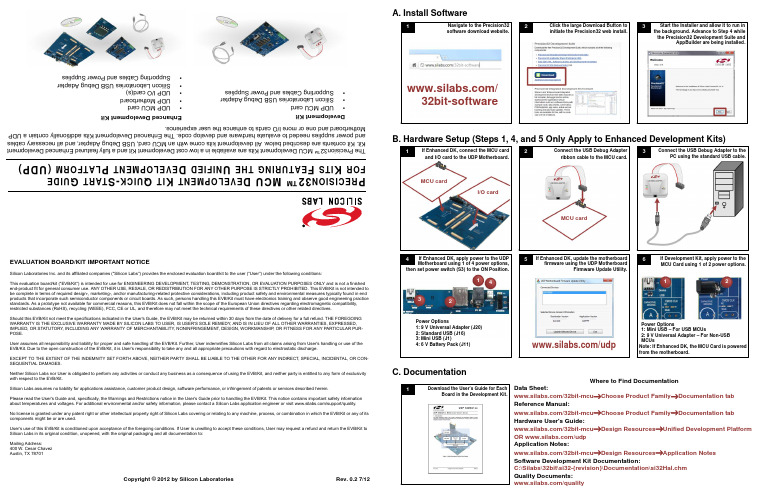
EVALUATION BOARD/KIT IMPORTANT NOTICESilicon Laboratories Inc. and its affiliated companies ("Silicon Labs") provides the enclosed evaluation board/kit to the user ("User") under the following conditions:This evaluation board/kit ("EVB/Kit") is intended for use for ENGINEERING DEVELOPMENT, TESTING, DEMONSTRATION, OR EVALUATION PURPOSES ONLY and is not a finished end-product fit for general consumer use. ANY OTHER USE, RESALE, OR REDISTRIBUTION FOR ANY OTHER PURPOSE IS STRICTLY PROHIBITED. This EVB/Kit is not intended to be complete in terms of required design-, marketing-, and/or manufacturing-related protective considerations, including product safety and environmental measures typically found in end products that incorporate such semiconductor components or circuit boards. As such, persons handling this EVB/Kit must have electronics training and observe good engineering practice standards. As a prototype not available for commercial reasons, this EVB/Kit does not fall within the scope of the European Union directives regarding electromagnetic compatibility, restricted substances (RoHS), recycling (WEEE), FCC, CE or UL, and therefore may not meet the technical requirements of these directives or other related directives.Should this EVB/Kit not meet the specifications indicated in the User's Guide, the EVB/Kit may be returned within 30 days from the date of delivery for a full refund. THE FOREGOING WARRANTY IS THE EXCLUSIVE WARRANTY MADE BY SILICON LABS TO USER, IS USER'S SOLE REMEDY , AND IS IN LIEU OF ALL OTHER WARRANTIES, EXPRESSED, IMPLIED, OR STATUTORY , INCLUDING ANY WARRANTY OF MERCHANTABILITY , NONINFRINGEMENT, DESIGN, WORKMANSHIP , OR FITNESS FOR ANY PARTICULAR PUR-POSE.User assumes all responsibility and liability for proper and safe handling of the EVB/Kit. Further, User indemnifies Silicon Labs from all claims arising from User's handling or use of the EVB/Kit. Due to the open construction of the EVB/Kit, it is User's responsibility to take any and all appropriate precautions with regard to electrostatic discharge.EXCEPT TO THE EXTENT OF THE INDEMNITY SET FORTH ABOVE, NEITHER PARTY SHALL BE LIABLE TO THE OTHER FOR ANY INDIRECT, SPECIAL, INCIDENTAL, OR CON-SEQUENTIAL DAMAGES.Neither Silicon Labs nor User is obligated to perform any activities or conduct any business as a consequence of using the EVB/Kit, and neither party is entitled to any form of exclusivity with respect to the EVB/Kit.Silicon Labs assumes no liability for applications assistance, customer product design, software performance, or infringement of patents or services described herein.Please read the User's Guide and, specifically, the Warnings and Restrictions notice in the User's Guide prior to handling the EVB/Kit. This notice contains important safety information about temperatures and voltages. For additional environmental and/or safety information, please contact a Silicon Labs application engineer or visit /support/quality.No license is granted under any patent right or other intellectual property right of Silicon Labs covering or relating to any machine, process, or combination in which the EVB/Kit or any of its components might be or are used.User's use of this EVB/Kit is conditioned upon acceptance of the foregoing conditions. If User is unwilling to accept these conditions, User may request a refund and return the EVB/Kit to Silicon Labs in its original condition, unopened, with the original packaging and all documentation to:Mailing Address:400 W. Cesar Chavez Austin, TX 78701Copyright © 2012 by Silicon Laboratories Rev. 0.2 7/12P R E C I S I O N 32™ M C U D E V E L O P M E N T K I T Q U I C K -S T A R T G U I D E F O R K I T S F E A T U R I N G T H E U N I F I E D D E V E L O P M E N T P L A T F O R M (U D P )T h e P r e c i s i o n 32™ M C U D e v e l o p m e n t K i t s a r e a v a i l a b l e i n a l o w c o s t D e v e l o p m e n t K i t a n d a f u l l y f e a t u r e d E n h a n c e d D e v e l o p m e n t K i t . K i t c o n t e n t s a r e d e s c r i b e d b e l o w . A l l d e v e l o p m e n t k i t s c o m e w i t h a n M C U c a r d , U S B D e b u g A d a p t e r , a n d a l l n e c e s s a r y c a b l e s a n d p o w e r s u p p l i e s n e e d e d t o e v a l u a t e h a r d w a r e a n d d e v e l o p c o d e . T h e E n h a n c e d D e v e l o p m e n t K i t s a d d i t i o n a l l y c o n t a i n a U D PM o t h e r b o a r d a n d o n e o r m o r e I /O c a r d s t o e n h a n c e t h e u s e r e x p e r i e n c e .D e v e l o p m e n t K i t•U D P M C U c a r d•S i l i c o n L a b o r a t o r i e s U S B D e b u g A d a p t e r •S u p p o r t i n g C a b l e s a n d P o w e r S u p p l i esE n h a n c e d D e v e l o p m e n t K i t•U D P M C U c a r d•U D P M o t h e r b o a r d •U D P I /O c a r d (s )•S i l i c o n L a b o r a t o r i e s U S B D e b u g A d a p t e r •S u p p o r t i n g C a b l e s a n d P o w e r S u p p l i e sA. Install SoftwareB. Hardware Setup (Steps 1, 4, and 5 Only Apply to Enhanced Development Kits)C. Documentation12Click the large Download Button to initiate the Precision32 web install.Navigate to the Precision32 software download website.3Start the Installer and allow it to run in the background. Advance to Step 4 while the Precision32 Development Suite andAppBuilder are being installed./32bit-software1Connect the USB Debug Adapter ribbon cable to the MCU card.2Connect the USB Debug Adapter to thePC using the standard USB cable.I/O cardMCU card45If Enhanced DK, apply power to the UDP Motherboard using 1 of 4 power options,Power Options1: 9 V Universal Adapter (J20)2: Standard USB (J16) 3: Mini USB (J1)4: 6 V Battery Pack (J11)then set power switch (S3) to the ON Position.If Development Kit, apply power to the MCU Card using 1 of 2 power options.Power Options1: Mini USB – For USB MCUs2: 9 V Universal Adapter – For Non-USB MCUsIf Enhanced DK, update the motherboardfirmware using the UDP MotherboardFirmware Update Utility./udpMCU card321412Note: If Enhanced DK, the MCU Card is powered from the motherboard.36If Enhanced DK, connect the MCU card and I/O card to the UDP Motherboard.1Download the User’s Guide for EachBoard in the Development Kit.Where to Find DocumentationData Sheet:/32bit-mcu →Choose Product Family →Documentation tab Reference Manual:/32bit-mcu →Choose Product Family →Documentation tab Hardware User's Guide:/32bit-mcu →Design Resources →Unified Development Platform OR /udp Application Notes:/32bit-mcu →Design Resources →Application Notes Software Development Kit Documentation:C:\Silabs\32bit\si32-{revision}\Documentation\si32Hal.chm Quality Documents:/qualityE . U s i n g t h e P r e c i s i o n 32 D e v e l o p m e n t S u i t eT h e P r e c i s i o n 32 D e v e l o p m e n t S u i t e i s a c o m p l e t e d e v e l o p m e n t s y s t e m f o r S i l i c o n L a b s 32-b i t M C U s . T h e D e v e l o p m e n t S u i t e c o n s i s t s o f t h r e e p a r t s : t h e U n i f i e d D e v e l o p m e n t P l a t f o r m (U D P ) h a r d w a r e , t h e S o f t w a r e D e v e l o p m e n t K i t (S D K ), a n d t h e P C d e v e l o p m e n t t o o l s i n c l u d i n g A p p B u i l d e r a n d t h e I n t e g r a t e d D e v e l o p m e n t E n v i r o n m e n t (I D E ). S e e t h e a p p l i c a t i o n n o t e s l i s t e d b e l o wf o r c o m p l e t e d e t a i l s .t h e p r o g r a m . T h e L E D b l i n k . P a u s e p r o g r a R u nl i n e s o f c o d e a n d s e l e c t T o g B r e a k p o i n t t o a d d a b r e a k p o T h e n p r e s s R u n t o r u n t o b r e a k p o i c o d e .S t e p I n t o o r S t e p O v e r V i e w o r m o d i f y P e r i p h e r a R e g i s t e r s , o r M e m o i a b l e , r i g h t -c l i a n d s e l e c t A d d W a t c h E x p r e t o a d d i t t o t h e E x p r e s s i o n s w A p p B u i l d e r I D E•A N 675: P r e c i s i o n 32 D e v e l o p m e n t S u i t e O v e r v i e w•A N 667: G e t t i n g S t a r t e d w i t h t h e S i l i c o n L a b s P r e c i s i o n 32 I D E•A N 670: G e t t i n g S t a r t e d w i t h t h e S i l i c o n L a b s P r e c i s i o n 32 A p p B u i l d e r•A N 678: P r e c i s i o n 32 s i 32F l a s h U t i l i t y C o m m a n d -L i n e P r o g r a m m e r U s e r 's G u i d e•A N 719: P r e c i s i o n 32 I D E a n d A p p B u i l d e r D e t a i l e d T u t o r i a l a n d W a l k t h r o u g hW h e r e t o F i n d S u p p o r tM C U K n o w l e d g e B a s e :w w w .s i l a b s .c o m →S u p p o r t →K n o w l e d g e B a s eV i d e o T r a i n i n g M o d u l e s :w w w .s i l a b s .c o m →S u p p o r t →T r a i n i n g a n d R e s o u r c e sC o n t a c t a n A p p l i c a t i o n s E n g i n e e r :w w w .s i l a b s .c o m →S u p p o r t →C o n t a c t T e c h n i c a l S u p p o r tD . U s i n g t h e P r e c i s i o n 32 I DE f o r t h eF i r s t T i m e2R e g i s t e r t h e I D E u s i n g t h e s t e p s l i s t e d o n t h e W e l c o m e p a g e .1O p e n t h e P r e c i s i o n 32 I D E a n d s e l e c t t h e p r o j e c t w o r k s p a c e .313456S e l e c t j u s t t h e s i m x x x x x _B l i n k y c h e c k b o x ,e n s u r e C o p y p r o j e c t s i n t o w o r k s p a c e i s s e l e c t e d , a n d p r e s s F i n i s h .S e l e c t t h e I m p o r t S I 32 S D Ke x a m p l e (s ) l i n k i n t h e Q u i c k s t a r t w i n d o w .S e l e c t t h e s i m x x x x x _B l i n k yp r o j e c t i n t h e P r o j e c t E x p l o r e r a n d p r e s s B u i l d ‘B l i n k y ’ [D e b u g ] i n t h e Q u i c k s t a r t w i n d o w .S t a r t a D e b u g s e s s i o n b yc l i c k i n g D e b u g ‘B l i n k y ’ [D e b u g ] i n t h e Q u i c k s t a r t w i nd o w .。
SPEAr320:工厂自动化嵌入式开发方案

・
S E r2 P A 3 0嵌入式微处理器 最 高 2Gbt D R23 3 z( i的 D 3 MH 标
准 1 8Mb t s) 2 ye
・
S i er a
I / F
・
最 高 1 ye 6Mb ts的串行 闪存 ( 标准 8
Mb t s) ye
・_ Jr AG调试端 口
更 多 详情 。敬 请 浏 览 :
ht P: I t / sOI i On. Ut eCCn. COm , s l t 2 1 3 1 5 5 5 . t ou i on 01 O1 O 0 6 1 5 h m
图 3 S Ar2 U评 估 板 方 框 图 PE 3 0CP
.
.
.
JE P G编解码器加速器 具有可编程预分频器的 ,6X1 6位
通 用 定 时 器 ,4个 捕 捉 输 入
ห้องสมุดไป่ตู้
。
一
具有 中断功能的 ,最高 1 2GPO 0 I
s E 3 o 用 P Ar2 应
S E 3 0嵌入 式微 处理 器是 可 P Ar2 配置的 ,适 用于工 业和消费类产 品。
・
US B2 O . H0S 1 T
・
两 个 U 20全 主 机 端 口通道 SB .
一
个 U 20主 机 设 备 端 口 SB .
・
一
USB20 .
HOS T2 US B2。 0
De i e vc
・
个 串行端 口 ( 最高 1 5b u 1 a d)
J AG b g p rs T De u o t
・
可编程逻辑控制器 工 厂 自动 化 打印机
- 1、下载文档前请自行甄别文档内容的完整性,平台不提供额外的编辑、内容补充、找答案等附加服务。
- 2、"仅部分预览"的文档,不可在线预览部分如存在完整性等问题,可反馈申请退款(可完整预览的文档不适用该条件!)。
- 3、如文档侵犯您的权益,请联系客服反馈,我们会尽快为您处理(人工客服工作时间:9:00-18:30)。
The EZ-KIT Lite evaluation system contains ESD (electrostatic discharge) sensitive devices. Electrostatic charges readily accumulate on the human body and equipment and can discharge without detection. Permanent damage may occur on devices subjected to high-energy discharges. Proper ESD precautions are recommended to avoid performance degradation or loss of functionality. Store unused EZ-KIT Lite boards in the protective shipping package.
ADSP-BF592 EZ-KIT Lite® Evaluation System Manual
Revision 1.1, July 2012 Part Number 82-000231-01
Analog Devices, Inc. One Technology Way Norwood, Mass. 02062-9106
Trademark and Service Mark Notice
The Analog Devices logo, Blackfin, CrossCore, EngineerZone, EZ-Extender, EZ-KIT Lite, and VisualDSP++ are registered trademarks of Analog Devices, Inc. All other brand and product names are trademarks or service marks of their respective owners.
CONTENTS
PREFACE
Product Overview ........................................................................... xi Purpose of This Manual ................................................................. xii Intended Audience ........................................................................ xiii Manual Contents .......................................................................... xiii What’s New in This Manual ........................................................... xiv Technical Support .......................................................................... xiv Supported Processors ....................................................................... xv Product Information ...................................................................... xvi Analog Devices Web Site .......................................................... xvi EngineerZone ........................................................................... xvi Related Documents ....................................................................... xvii Notation Conventions ................................................................... xvii
ADSP-Bm Manual
v
Contents
VisualDSP++ Install and Session Startup ....................................... 1-8 Session Startup ........................................................................ 1-8 CCES Evaluation License ........................................................... 1-10 VisualDSP++ Evaluation License ................................................. 1-11 Memory Map ............................................................................. 1-12 SPI Flash Memory Interface ........................................................ 1-13 Audio Interface ........................................................................... 1-13 Power-On-Self Test ..................................................................... 1-14 Expansion Interface II ................................................................. 1-14 Power Architecture ..................................................................... 1-15 VDDINT Programmable Regulator ............................................ 1-16 Power Measurements .................................................................. 1-17 Board Design Database ............................................................... 1-18 Example Programs ...................................................................... 1-18
Disclaimer
Analog Devices, Inc. reserves the right to change this product without prior notice. Information furnished by Analog Devices is believed to be accurate and reliable. However, no responsibility is assumed by Analog Devices for its use; nor for any infringement of patents or other rights of third parties which may result from its use. No license is granted by implication or otherwise under the patent rights of Analog Devices, Inc.
Regulatory Compliance
The ADSP-BF592 EZ-KIT Lite is designed to be used solely in a laboratory environment. The board is not intended for use as a consumer end product or as a portion of a consumer end product. The board is an open system design which does not include a shielded enclosure and therefore may cause interference to other electrical devices in close proximity. This board should not be used in or near any medical equipment or RF devices. The ADSP-BF592 EZ-KIT Lite has been certified to comply with the essential requirements of the European EMC directive 2004/108/EC and therefore carries the “CE” mark. The ADSP-BF592 EZ-KIT Lite has been appended to Analog Devices, Inc. EMC Technical File (EMC TF) referenced DSPTOOLS1, issue 2 dated June 4, 2008 and was declared CE compliant by an appointed Notified Body (No.0673) as listed below. Notified Body Statement of Compliance: Z600ANA2.039 dated June 22 2010. Issued by: Technology International (Europe) Limited 56 Shrivenham Hundred Business Park Shrivenham, Swindon, SN6 8TY, UK